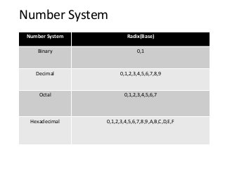
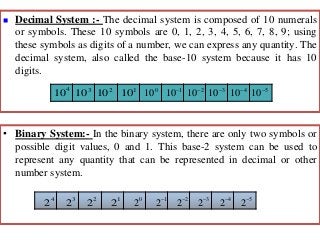
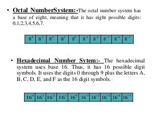
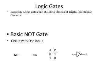
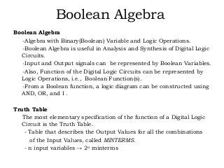
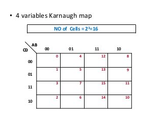
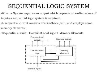
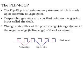
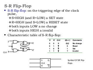
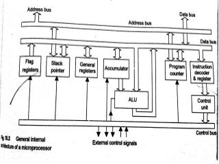
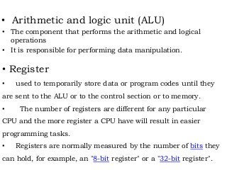
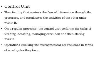
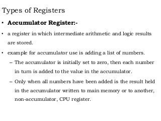
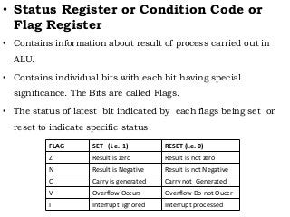
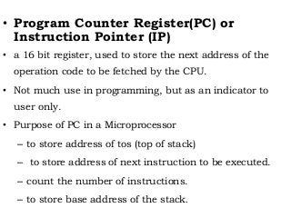
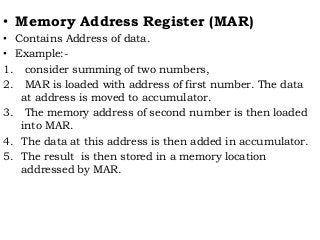
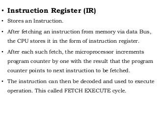
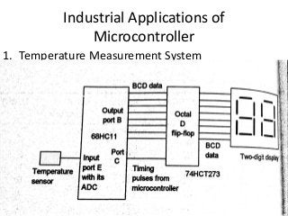
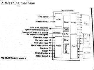
2. Number System
Number System Radix(Base)
Binary 0,1
Decimal 0,1,2,3,4,5,6,7,8,9
Octal 0,1,2,3,4,5,6,7
Hexadecimal 0,1,2,3,4,5,6,7,8,9,A,B,C,D,E,F
3. Decimal System :- The decimal system is composed of 10 numerals
or symbols. These 10 symbols are 0, 1, 2, 3, 4, 5, 6, 7, 8, 9; using
these symbols as digits of a number, we can express any quantity. The
decimal system, also called the base-10 system because it has 10
digits.
4
10 3
10 2
10 1
10 0
10 1
10 2
10 3
10 4
10 5
10
• Binary System:- In the binary system, there are only two symbols or
possible digit values, 0 and 1. This base-2 system can be used to
represent any quantity that can be represented in decimal or other
number system.
4
2 3
2 2
2 1
2 0
2 1
2 2
2 3
2 4
2 5
2
4. • Octal NumberSystem:-The octal number system has
a base of eight, meaning that it has eight possible digits:
0,1,2,3,4,5,6,7.
4
8 3
8 2
8 1
8 0
8 1
8 2
8 3
8 4
8 5
8
• Hexadecimal Number Sytem:- The hexadecimal
system uses base 16. Thus, it has 16 possible digit
symbols. It uses the digits 0 through 9 plus the letters A,
B, C, D, E, and F as the 16 digit symbols.
4
16 3
16 2
16 1
16 0
16 1
16 2
16 3
16 4
16 5
16
5. Logic Gates
• Basically Logic gates are Building Blocks of Digital Electronic
Circuits.
• Basic NOT Gate
• Circuit with One input
NOT P=A A P
A P
0 1
1 0
6. • Circuits with two Inputs
AND P = X.Y
OR P= X+Y
x
y
xy
x+yx
y
X Y P
0 0 0
0 1 0
1 0 0
1 1 1
X Y P
0 0 0
0 1 1
1 0 1
1 1 1
Basic AND and OR
7. Basic NAND and NOR
• Circuits with two Inputs
NAND P = X.Y
NOR P= X+Y
x
y
xy
x+yx
y
X Y P
0 0 1
0 1 1
1 0 1
1 1 0
X Y P
0 0 1
0 1 0
1 0 0
1 1 0
8. Basic XOR and XNOR
• Circuits with two Inputs:
XOR P = X Y
XNOR P = A B
xyx
y
A
B
P
X Y P
0 0 0
0 1 1
1 0 1
1 1 0
A B P
0 0 0
0 1 1
1 0 1
1 1 0
9. Boolean Algebra
Boolean Algebra
-Algebra with Binary(Boolean) Variable and Logic Operations.
-Boolean Algebra is useful in Analysis and Synthesis of Digital Logic
Circuits.
-Input and Output signals can be represented by Boolean Variables.
-Also, Function of the Digital Logic Circuits can be represented by
Logic Operations, i.e., Boolean Function(s).
-From a Boolean function, a logic diagram can be constructed using
AND, OR, and I .
Truth Table
The most elementary specification of the function of a Digital Logic
Circuit is the Truth Table.
- Table that describes the Output Values for all the combinations
of the Input Values, called MINTERMS.
- n input variables → 2n minterms
10. Boolean Algebraic Laws
(A.B).C = A.B.C = A.(B.C)Associative
A.(B + C) = A.B + A.C
A + (B.C) = (A + B).(A + C)
Distributive
A . B = B . A
A + B = B + A
Commutative
A . 0 = 0 A . 1 = A
A + 0 = A A + 1 = 1
Operating with logic 0 and logic 1
A . A = 0
A + A = 1
Complementary
A . A = A
A + A = A
Tautology (Idempotent)
11. KARNAUGH MAPS
• Named for the American electrical
engineer Maurice Karnaugh
• Karnaugh maps provide an alternative
way of simplifying logic circuits.
• Instead of using Boolean algebra
simplification techniques, you can
transfer logic values from a Boolean
statement or a truth table into a
Karnaugh map.
• The arrangement of 0's and 1's within
the map helps you to visualise the logic
relationships between the variables and
leads directly to a simplified Boolean
statement.
12. • Karnaugh maps, or K-maps, are often used to
simplify logic problems with 2, 3 or 4 variables.
No of Cells = 2n
(where n is a number of variables)
For the case of 2 variables, we form a map consisting of 22=4 cells as
shown in Figure
BA+ BA +
BA+ BA +
00 10
01 11
BA+ BA +
BA+ BA +
0 2
1 3
BA
BA AB
BA
A
B
0 1
0
1
A
B
0 1
0
1
A
B
0 1
0
1
13. • 3 variables Karnaugh map
NO of Cells = 23=8
AB
C 00 01 11 10
0
1
CBA CBA CAB CBA
CBA BCA ABC CBA
0 2 6 4
531 7
14. • 4 variables Karnaugh map
AB
CD 00 01 11 10
00
01
11
10
5
3
1
7
62
0 4
9
15
13
11
1014
12 8
NO of Cells = 23=16
15. SEQUENTIAL LOGIC SYSTEM
•When a System requires an output which depends on earlier values of
inputs a sequential logic system is required.
•A sequential circuit consists of a feedback path, and employs some
memory elements.
•Sequential circuit = Combinational logic + Memory Elements
Combinational
logic
Memory
elements
Combinational
outputs Memory outputs
External inputs
16. The FLIP-FLOP
• The Flip-Flop is a basic memory element which is made
up of assembly of Logic gates.
• Output changes state at a specified point on a triggering
input called the clock.
• Change state either at the positive edge (rising edge) or at
the negative edge (falling edge) of the clock signal.
Positive edges Negative edges
Clock signal
17. S-R Flip-Flop
S-R flip-flop: on the triggering edge of the clock
pulse,
S=HIGH (and R=LOW) a SET state
R=HIGH (and S=LOW) a RESET state
both inputs LOW a no change
both inputs HIGH a invalid
Characteristic table of S-R flip-flop:
S
Q
Q'
R
S R CLK Q(t+1) Comments
0 0 X Q(t) No change
0 1 0 Reset
1 0 1 Set
1 1 ? Invalid
CLK
S Q
CLK
R Q
Symbol Of SR Flip-
Flops
18. J-K Flip Flop
• For many applications the indeterminate state that occurs with SR
Flip-Flops when S=1 and R=1 is invalid then another form of Flip
Flop is used called J-K Flip Flop.
• The main difference between SR and JK Flip Flops is that there is no
Invalid state in JK Flip Flop.
• Include a toggle state.
J=HIGH (and K=LOW) a SET state
K=HIGH (and J=LOW) a RESET state
both inputs LOW a no change
both inputs HIGH a toggle
20. D Flip-flop
Basically a clocked SR Flip Flop or JK Flip Flop with D input
directly connected to S or J Input and via NOT gate to R or K
gate.
D flip-flop: single input D (data)
D=HIGH a SET state
D=LOW a RESET state
S
C
R
Q
Q'
CLK
D
D CLK Q(t+1) Comments
1 1 Set
0 0 Reset
21. REGISTERS
• A register is a set of memory elements and is used to hold
information till it is needed.
• It can be done by using set of Flip Flops.
• The register using D Flip Flop is shown below:
* After occurrence of negative-going
transition
Q1 =
X*
D
CLK
Q
Q'
Q2 =
Y*
D
CLK
Q
Q'
Q3 =
Z*
D
CLK
Q
Q'
Combinational
logic circuit
Transfer
X
Y
Z
22. • When Load signal is 0, NO clock input occurs to
D Flip Flops and so no change occurs to the
state of Flip Flops.
• When Load signal is 1 then the input can
change the states of Flip Flops.
• As long as load signal is 0 the FLIP FLOPS will
HOLD their OLD STATE VALUES.
23. Microprocessors
• A computer is a programmable machine that receives
input, stores and manipulates data/Information, and
provides output in a useful format.
• The microprocessor can be programmed to perform
functions on given data by writing specific instructions
into its memory.
– The microprocessor reads one instruction at a time,
matches it with its instruction set, and performs the
data manipulation specified.
– The result is either stored back into memory or
displayed on an output device.
24. Basic Components of
Microprocessor system
Microprocessor system has folllowing three parts
1. CPU - Central Processing Unit:-
the portion of a computer system that carries out the
instructions of a computer program
2. Input/output (I/O):-
refers to the communication between a computer and
the outside world possibly a human, or another
information processing system.
3. Memory:-
physical devices used to store data or programs
(sequences of instructions) on a temporary or
permanent basis.
25. The MICROPROCESSOR
• Generally referred to as Central Processing Unit (CPU).
• It is that part which fetches, decodes and executes an
information
• The following figure illustrates block diagram of
microprocessor
ALU Register
Section
Control and timing section
Address bus
Data bus
Control bus
26.
27. • Arithmetic and logic unit (ALU)
• The component that performs the arithmetic and logical
operations
• It is responsible for performing data manipulation.
• Register
• used to temporarily store data or program codes until they
are sent to the ALU or to the control section or to memory.
• The number of registers are different for any particular
CPU and the more register a CPU have will result in easier
programming tasks.
• Registers are normally measured by the number of bits they
can hold, for example, an "8-bit register" or a "32-bit register".
28. • Control Unit
• The circuitry that controls the flow of information through the
processor, and coordinates the activities of the other units
within it.
• On a regular processor, the control unit performs the tasks of
fetching, decoding, managing execution and then storing
results.
• Operations involving the microprocessor are reckoned in terms
of no of cycles they take.
29. Types of Registers
• Accumulator Register:-
• a register in which intermediate arithmetic and logic results
are stored.
• example for accumulator use is adding a list of numbers.
– The accumulator is initially set to zero, then each number
in turn is added to the value in the accumulator.
– Only when all numbers have been added is the result held
in the accumulator written to main memory or to another,
non-accumulator, CPU register.
30. • Status Register or Condition Code or
Flag Register
• Contains information about result of process carried out in
ALU.
• Contains individual bits with each bit having special
significance. The Bits are called Flags.
• The status of latest bit indicated by each flags being set or
reset to indicate specific status.
FLAG SET (i.e. 1) RESET (i.e. 0)
Z Result is zero Result is not zero
N Result is Negative Result is not Negative
C Carry is generated Carry not Generated
V Overflow Occurs Overflow Do not Ouccr
I Interrupt ignored Interrupt processed
31. • Program Counter Register(PC) or
Instruction Pointer (IP)
• a 16 bit register, used to store the next address of the
operation code to be fetched by the CPU.
• Not much use in programming, but as an indicator to
user only.
• Purpose of PC in a Microprocessor
– to store address of tos (top of stack)
– to store address of next instruction to be executed.
– count the number of instructions.
– to store base address of the stack.
32. • Memory Address Register (MAR)
• Contains Address of data.
• Example:-
1. consider summing of two numbers,
2. MAR is loaded with address of first number. The data
at address is moved to accumulator.
3. The memory address of second number is then loaded
into MAR.
4. The data at this address is then added in accumulator.
5. The result is then stored in a memory location
addressed by MAR.
33. • Instruction Register (IR)
• Stores an Instruction.
• After fetching an instruction from memory via data Bus,
the CPU stores it in the form of instruction register.
• After each such fetch, the microprocessor increments
program counter by one with the result that the program
counter points to next instruction to be fetched.
• The instruction can then be decoded and used to execute
operation. This called FETCH EXECUTE cycle.
34. • General Purpose Register
• May serve as temporary storage for data and address and
used in operations involving transfer between other
registers.
• Stack Pointer Register
• The contents of this register form an address which
defines the top stack of in RAM.
• It is a special area of the memory in which program
counter values can be stored when a subroutine part of a
program is being used i.e. pushing the return address on
a jump, and retrieving it after the operation is complete
to come back to its original location.
35. INTEL 8085A
Development of earlier 8080 processor.
Six general purpose 8-bit registers: B, C, D, E, H, L
They can also be combined as register pairs to
perform 16-bit operations: BC, DE, HL
Registers are programmable (data load, move, etc.)
Accumulator
Single 8-bit register that is part of the ALU !
Used for arithmetic / logic operations – the result is
always stored in the accumulator.
36. The internal architecture of the 8085 CPU is capable of performing the
following operations:
Store 8-bit data (Registers, Accumulator)
Perform arithmetic and logic operations (ALU)
Test for conditions (IF / THEN)
Sequence the execution of instructions
Store temporary data in RAM during execution
37.
38. Microcontrollers
• Microcontroller is an integration of a
microprocessor with memory and Input-
Output interfaces.
• It has pins for external connections of input
and output, power, clock and control signals.
• The pins for input and output are grouped
into units called input-output ports.
• To transmit data there are lines on the ports
for 8-bit – Single port
for 16-bit- Double Ports
40. Basic I/O Concepts
• Peripherals such as LEDs and keypads are
essential components of microcontroller-
based systems
• Input devices
– Provide digital information to an MPU (Memory
protection Unit).
– Examples: switch, keyboard, scanner, and
digital camera
• Output devices
– Receive digital information from an MPU.
– Examples: LED, seven-segment display, LCD,
and printer
• Devices are interfaced to an MPU using I/O
ports.
44. Digital-to-Analog Conversion
• When data is in binary form, the 0's and 1's
may be of several forms such as the TTL form
where the logic zero may be a value up to 0.8
volts and the 1 may be a voltage from 2 to 5
volts.
• The data can be converted to clean digital
form using gates which are designed to be on
or off depending on the value of the incoming
signal.
45.
46. Analog-to-Digital Conversion
• The basic principle of operation is to use the
comparator principle to determine whether or
not to turn on a particular bit of the binary
number output.
• It is typical for an ADC to use a digital-to-
analog converter (DAC) to determine one of
the inputs to the comparator
47.
48. Elements(Hardware) in Mechatronics
System
• Principle elements of Mechatronics System are
• Mechanical Elements:-
Refers to Mechanical Structure, Mechanism, Thermo Fluid,
Hydraulic aspects of Mechanical system.
• Electro-Mechanical Elements:-
Refers to Sensors And Actuators
• Electrical / Electronic Elements:-
Refers to electrical components like capacitor, Inductor,
transformer, Circuits etc.
49. • Control interface/Computing hardware Elements:-
Refers to Analog-to-Analog convertor, Digital-to-Analog
Convertor, I/P-O/P system, Counters, Timers etc.
• Computer:-
Refers to Hardware/Software utilized to perform Computer
aided dynamics system analysis, Optimization, Design and
Simulation etc.