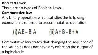
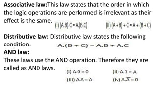
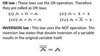
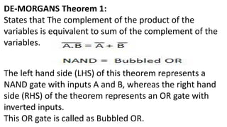
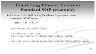
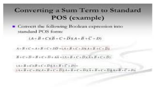
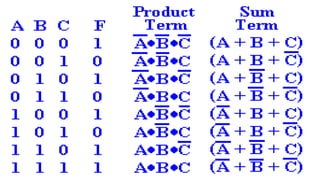
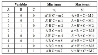
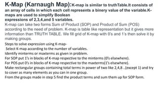
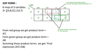
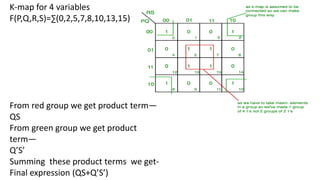
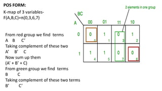
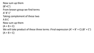
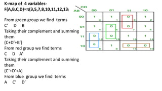
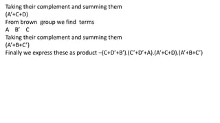
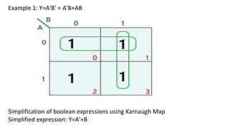
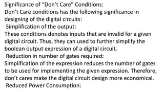
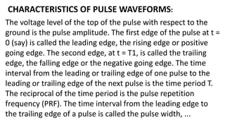
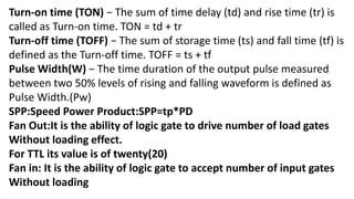
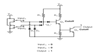
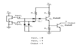
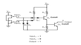
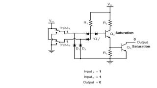
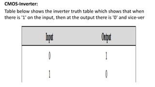
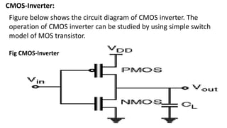
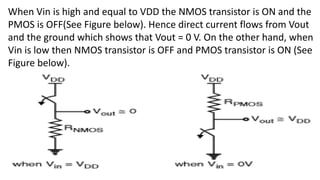
BSc II SEM ELE-2 UNIT-2
BOOLEAN ALGEBRA
Boolean algebra is a division of mathematics that deals
with operations on logical values and incorporates
binary variables. Boolean algebra traces its origins to an
1854 book by mathematician George Boole.
The distinguishing factor of Boolean algebra is that it
deals only with the study of binary variables. Most
commonly Boolean variables are presented with the
possible values of 1 ("true") or 0 ("false"). Variables can
also have more complex interpretations, such as in set
theory. Boolean algebra is also known as binary algebra.
Logic gates are the basic building blocks of any digital
system. It is an electronic circuit having one or more
than one input and only one output. The relationship
between the input and the output is based on a certain
logic. Based on this, logic gates are named as AND gate,
OR gate, NOT gate Called Basic gates
AND Gate
A circuit which performs an AND operation is shown in
figure. It has n input (n >= 2) and one output.
AND gate
AND Logical Diagram
AND Truth Table
OR Gate: A circuit which performs an OR operation is
shown in figure. It has n input (n >= 2) and one output.
Logic diagram Truth Table
NOT Gate: NOT gate is also known as Inverter. It has one
input A and one output Y.
Logic diagram Truth Table
Positive and Negative logic in Digital Electronics
Basic difference between positive and negative logic
There are two types of representations used in digital
systems, the positive logic and the negative logic
representations.
In positive logic representation Bit 1 represents Logic
high and Bit 0 represent a Logic low as shown in fig 2 a
and b. High is represented by +5 Volts and low is
represented by -5 Volts or 0 Volts.
In Negative logic representation Bit 1 represents logic low and
Bit 0 represents logic high as shown in Fig 3 a and b. In terms of
voltage level, bit 1 can be represented as +5V and bit 0 can be
represented as 0 V or -5 Volts
Boolean Laws:
There are six types of Boolean Laws.
Commutative law
Any binary operation which satisfies the following
expression is referred to as commutative operation.
Commutative law states that changing the sequence of
the variables does not have any effect on the output of
a logic circuit.
Associative law:This law states that the order in which
the logic operations are performed is irrelevant as their
effect is the same.
Distributive law: Distributive law states the following
condition.
AND law:
These laws use the AND operation. Therefore they are
called as AND laws.
OR law : These laws use the OR operation. Therefore
they are called as OR laws.
INVERSION law : This law uses the NOT operation. The
inversion law states that double inversion of a variable
results in the original variable itself.
DE-MORGANS Theorem 1:
States that The complement of the product of the
variables is equivalent to sum of the complement of the
variables.
The left hand side (LHS) of this theorem represents a
NAND gate with inputs A and B, whereas the right hand
side (RHS) of the theorem represents an OR gate with
inverted inputs.
This OR gate is called as Bubbled OR.
Table showing verification of the De Morgan's first
theorem −
DE- Morgans Theorem 2 : States that the sum of the
Complements of the Variables is equivalent to the
DERIVED LOGIC GATES: NAND Gate
A NOT-AND operation is known as NAND operation. It
has n input (n >= 2) and one output.
NAND gate
Logic diagram Truth Table
NOR Gate: A NOT-OR operation is known as NOR
operation. It has n input (n >= 2) and one output.
Logic diagram Truth Table
XOR Gate: XOR or Ex-OR gate is a special type of gate. It
can be used in the half adder, full adder and subtractor.
The exclusive-OR gate is abbreviated as EX-OR gate or
sometime as X-OR gate. It has n input (n >= 2) and one
output.
Logic diagram Truth Table
XNOR Gate : XNOR gate is a special type of gate. It can
be used in the half adder, full adder and subtractor. The
exclusive-NOR gate is abbreviated as EX-NOR gate or
sometime as X-NOR gate. It has n input (n >= 2) and one
output.
Logic diagram Truth Table
UNIVERSAL LOGIC GATES: NAND and NOR Gates are
Called Universal gates since with these gates all logic
gates are constructed.Universal property of NAND gate:
Universal property of NOR Logic gate:
Equivalency of Logic gate:
NAND Logic gate is equivalent to negative OR gate
And NOR Logic gate is equivalent to negative and gate.
K-Map (Karnaugh Map):K-map is similar to truthTable.It consists of
an array of cells in which each cell represents a binery value of the variable.K-
maps are used to simplify Boolean
expressions of 2,3,4,and 5 variables.
K-map can take two forms Sum of Product (SOP) and Product of Sum (POS)
according to the need of problem. K-map is table like representation but it gives more
information than TRUTH TABLE. We fill grid of K-map with 0’s and 1’s then solve it by
making groups.
Steps to solve expression using K-map-
Select K-map according to the number of variables.
Identify minterms or maxterms as given in problem.
For SOP put 1’s in blocks of K-map respective to the minterms (0’s elsewhere).
For POS put 0’s in blocks of K-map respective to the maxterms(1’s elsewhere).
Make rectangular groups containing total terms in power of two like 2,4,8 ..(except 1) and try
to cover as many elements as you can in one group.
From the groups made in step 5 find the product terms and sum them up for SOP form.
SOP FORM :
K-map of 3 variables-
Z= ∑A,B,C(1,3,6,7)
From red group we get product term—
A’C
From green group we get product term—
AB
Summing these product terms we get- Final
expression (A’C+AB)
K-map for 4 variables
F(P,Q,R,S)=∑(0,2,5,7,8,10,13,15)
From red group we get product term—
QS
From green group we get product
term—
Q’S’
Summing these product terms we get-
Final expression (QS+Q’S’)
POS FORM:
K-map of 3 variables-
F(A,B,C)=π(0,3,6,7)
From red group we find terms
A B C’
Taking complement of these two
A’ B’ C
Now sum up them
(A’ + B’ + C)
From green group we find terms
B C
Taking complement of these two terms
B’ C’
Now sum up them
(B’+C’)
From brown group we find terms
A’ B’ C’
Taking complement of these two
A B C
Now sum up them
(A + B + C)
We will take product of these three terms :Final expression (A’ + B’ + C) (B’ + C’)
(A + B + C)
K-map of 4 variables-
F(A,B,C,D)=π(3,5,7,8,10,11,12,13)
From green group we find terms
C’ D B
Taking their complement and summing
them
(C+D’+B’)
From red group we find terms
C D A’
Taking their complement and summing
them
(C’+D’+A)
From blue group we find terms
A C’ D’
Taking their complement and summing them
(A’+C+D)
From brown group we find terms
A B’ C
Taking their complement and summing them
(A’+B+C’)
Finally we express these as product –(C+D’+B’).(C’+D’+A).(A’+C+D).(A’+B+C’)
Example 1: Y=A'B' + A'B+AB
Simplification of boolean expressions using Karnaugh Map
Simplified expression: Y=A'+B
Example 2: Y=A'B'C'+A' BC'+AB' C'+AB' C+ABC'+ABC
Simplification of boolean expressions using Karnaugh Map
Simplified expression: Y=A+C'
Example 3: Y=A'B'C' D'+A' B' CD'+A' BCD'+A' BCD+AB' C' D'+ABCD'+ABCD
Simplification of boolean expressions using Karnaugh Map
Simplified expression: Y=BD+B'D'
Example 1: Y=(A'+B')+(A'+B)+(A+B)
Simplification of boolean expressions using Karnaugh Map
Simplified expression: A'B
Example 2: Y=(A + B + C') + (A + B' + C') + (A' + B' + C) + (A' + B' + C')
Simplification of boolean expressions using Karnaugh Map
Simplified expression: Y=(A + C') .(A' + B')
Example 3: F(A,B,C,D)=π(3,5,7,8,10,11,12,13)
Simplification of boolean expressions using Karnaugh Map
Simplified expression: Y=(A + C') .(A' + B')
Don’t Care (X) Conditions in K-Maps:
One of the very significant and useful concept in simplifying the output
expression using K-Map is the concept of “Don’t Cares”. The “Don’t
Care” conditions allow us to replace the empty cell of a K-Map to form
a grouping of the variables which is larger than that of forming groups
without don’t cares. While forming groups of cells, we can consider a
“Don’t Care” cell as 1 or 0 or we can also ignore that cell. Therefore,
“Don’t Care” condition can help us to form a larger group of cells.
A Don’t Care cell can be represented by a cross(X) in K-Maps
representing a invalid combination. For example, in Excess-3 code
system, the states 0000, 0001, 0010, 1101, 1110 and 1111 are invalid
or unspecified. These states are called don’t cares.
.
A standard SOP function having don’t cares can be converted into a
POS expression by keeping don’t cares as they are, and writing the
missing minterms of the SOP form as the maxterm of POS form.
Similarly, a POS function having don’t cares can be converted to SOP
form keeping the don’t cares as they are and writing the missing
maxterms of the POS expression as the minterms of SOP expression.
Example-1:
Minimise the following function in SOP minimal form using K-Maps:
f = m(1, 5, 6, 11, 12, 13, 14) + d(4)
Explanation:
The SOP K-map for the given expression is:
Therefore, SOP minimal is,
f = BC' + BD' + A'C'D + AB'CD
Example-2: Minimise the following function in POS minimal form using
K-Maps: F(A, B, C, D) = m(0, 1, 2, 3, 4, 5) + d(10, 11, 12, 13, 14, 15)
Explanation: Writing the given expression in POS form:
F(A, B, C, D) = M(6, 7, 8, 9) + d(12, 13, 14, 15)
The POS K-map for the given expression is:
Therefore, POS minimal is,
F = (A'+ C)(B' + C')
Example-3: Minimise the following function in SOP minimal form using
K-Maps: F(A, B, C, D) = m(1, 2, 6, 7, 8, 13, 14, 15) + d(0, 3, 5, 12)
Explanation: The SOP K-map for the given expression is:
Therefore,
f = AC'D' + A'D + A'C + AB
Significance of “Don’t Care” Conditions:
Don’t Care conditions has the following significance in
designing of the digital circuits:
Simplification of the output:
These conditions denotes inputs that are invalid for a given
digital circuit. Thus, they can used to further simplify the
boolean output expression of a digital circuit.
Reduction in number of gates required:
Simplification of the expression reduces the number of gates
to be used for implementing the given expression. Therefore,
don’t cares make the digital circuit design more economical.
Reduced Power Consumption:
While grouping the terms long with don’t cares reduces
switching of the states. This decreases the memory space that
is required to represent a given digital circuit which in turn
results in less power consumption.
Represent Invalid States in Code Converters:
These are used in code converters. For example- In design of 4-
bit BCD-to-XS-3 code converter, the input combinations 1010,
1011, 1100, 1101, 1110, and 1111 are don’t cares.
Prevention of Hazards in Digital Circuits:
Don’t cares also prevents hazards in digital systems.
CHARACTERISTICS OF PULSE WAVEFORMS:
The voltage level of the top of the pulse with respect to the
ground is the pulse amplitude. The first edge of the pulse at t =
0 (say) is called the leading edge, the rising edge or positive
going edge. The second edge, at t = T1, is called the trailing
edge, the falling edge or the negative going edge. The time
interval from the leading or trailing edge of one pulse to the
leading or trailing edge of the next pulse is the time period T.
The reciprocal of the time period is the pulse repetition
frequency (PRF). The time interval from the leading edge to
the trailing edge of a pulse is called the pulse width, ...
CHARACTERISTICS OF PULSE WAVEFORMS
Duty cycle − Ratio of the pulse width to the period D=(Pw/T)*100%
Rise time − Time it takes to rise from 10% to 90% of its maximum
amplitude. (tr)
Time delay(td) − The time taken by the out put current to reach
from its initial value to 10% of its final value is called as the Time
Delay.
Fall time (tf) − The time taken for the collector current to reach from
90% of its maximum value to 10% of its initial value is called as the
Fall Time.
Storage time (ts) − The time interval between the trailing edge of the
input pulse to the 90% of the maximum value of the output, is called
as the Storage time.
Turn-on time (TON) − The sum of time delay (td) and rise time (tr) is
called as Turn-on time. TON = td + tr
Turn-off time (TOFF) − The sum of storage time (ts) and fall time (tf) is
defined as the Turn-off time. TOFF = ts + tf
Pulse Width(W) − The time duration of the output pulse measured
between two 50% levels of rising and falling waveform is defined as
Pulse Width.(Pw)
SPP:Speed Power Product:SPP=tp*PD
Fan Out:It is the ability of logic gate to drive number of load gates
Without loading effect.
For TTL its value is of twenty(20)
Fan in: It is the ability of logic gate to accept number of input gates
Without loading
Logic Families
Digital ICs are made of logic gates with suitable technology called Logic
families. Types of logic families are:
The digital ICs are designed using any of either bipolar devices or MOS
or a combination of both. The logic families which fall under the first
kind are called bipolar families, this include diode logic (DL), emitted
coupled logic (ECL), resistor transistor logic (RTL), diode transistor
logic (DTL), transistor transistor logic (TTL). The members of other
logic family i.e. MOS family are PMOS, NMOS family, CMOS family.
Now the Bi-MOS logic family is the one that uses both bipolar and
MOS devices.
TTL sub families. The TTL family consists of various subfamilies such as
standard TTL, low-power TTL, high power TTL, low power Schottky
TTL, Schottky TTL, advanced low-power Schottky TTL, advanced
Schottky TTL and fast TTL. The ICs which belong to TTL family are
designated as follows – 74 or 54 for standard TTL, 74L or 54L for low-
power TTL, 74H or 54H for high power TTL, 74LS or 54LS for Low
power schottky TTL and so on.
CMOS subfamilies:This is a popular logic family which includes 4000A,
4000B, 4000UB, 54/74C, 54/74HC, 54/74HCT, 54/74AC and 54/74ACT
families. The subfamilies are divided on the basis of voltage difference
and other parameters.
ECL Subfamilies:
ECL stands for Emitter Coupled Logic family and it was introduced by
ON semiconductor in 1962. The first product launched of this family
was MECL-1 series. Later MECL-II, MECL-III, MECL-10K, MECL-10H
series came into existence.
ECL Subfamilies:
TTL NAND gate and its operation:
Operation of TTL NAND Gate: Fig.(d) Demonstrates a TTL NAND gate with a totem
pole output. The totem pole output implies that transistor T4 sits atop T3 in
order to give low output impedance. The low output impedance means a short
time constant RC therefore the output can change rapidly from one state to the
other. T1 is a multiple type emitter transistor. Such transistor can be thought of like
a combination of various transistors along with a common collector and base.
Multiple emitter transistors along with about 60 emitters have been developed. In
this figure, T1 has 3 emitters thus there can be three inputs A, B, C. The transistor
T2 functions as a phase splitter since the emitter voltage is out of phase along with
the collector voltage. The transistors T3 and T4 by the totem pole output, the
capacitance CL shows the stray capacitance and so on. The diode D is added to
make sure that T4 is cut off while output is low. The voltage drop of diode D
remains the base-emitter junction of T4 reverse biased therefore only T3 conducts
while output is low. The operation can be described briefly by three conditions as
specified below:
Condition 1: At least one input is low (that is, 0). Transistor T1 saturates. Thus,
the base voltage of T2 is almost zero. T2 is cut off and forces T3 to cut off. T4
functions as an emitter follower and couples a high voltage to load. Output is high
(that is Y=1).
Condition 2: Each input is high. The emitter base junctions of T1 are reverse
biased. The collector base junction of T1 is forward biased. Therefore, T1 is in
reverse active mode. The collector current of T1 flows in reverse direction.
Because this current is flowing in the base of T2, the transistors T2 and T3
saturate and then output Y is low.
Condition 3: The circuit is operating under II while one of the inputs becomes low.
The consequent emitter base junction of T1 starts conducting and T1 base voltage
drops to a low value. Thus, T1 is in forward active mode. The high collector
current of T1 shifts the stored charge in T2 and T3 and hence, T2 and T3 go to cut-
off and T1 saturates and then output Y returns to high.
Fig.(d) Logic Diagram of TTL NAND Gate with Totem Pole Output
TTL NAND gate with open collector:
Since this circuit bears so much resemblance to the simple inverter circuit, the
only difference being a second input terminal connected in the same way to the
base of transistor Q2, we can say that each of the inputs will have the same
effect on the output.Namely, if either of the inputs is grounded, transistor Q2 will
be forced into a condition of cutoff, thus turning Q3 off and floating the output
(output goes “high”). The following series of illustrations shows this for three
input states (00, 01, and 10):
In any case, where there is a grounded (“low”) input, the output is guaranteed
to be floating (“high”). Conversely, the only time the output will ever go “low” is
if transistor Q3 turns on, which means transistor Q2 must be turned on
(saturated), which means neither input can be diverting R1current away from
the base of Q2. The only condition that will satisfy this requirement is when
both inputs are “high” (1):
CMOS-Inverter:
Table below shows the inverter truth table which shows that when
there is '1' on the input, then at the output there is '0' and vice-ver
CMOS-Inverter:
Fig CMOS-Inverter
Figure below shows the circuit diagram of CMOS inverter. The
operation of CMOS inverter can be studied by using simple switch
model of MOS transistor.
When Vin is high and equal to VDD the NMOS transistor is ON and the
PMOS is OFF(See Figure below). Hence direct current flows from Vout
and the ground which shows that Vout = 0 V. On the other hand, when
Vin is low then NMOS transistor is OFF and PMOS transistor is ON (See
Figure below).
Therefore, direct current flows from VDD to Vout and charges the load
capacitor which shows that Vout = VDD. Therefore the circuit works as
an inverter (See Table).
Properties of CMOS Inverter :
(1) Since in CMOS inverter there is existence of direct between power
supply and ground, it has low output impedance.
(2) As the output voltage in CMOS inverter is always either VDD or
GND, the voltage swing in CMOS inverter is VDD 0, hence VDD .
(3) As the gate of MOS transistor does not draws any DC input current
the input resistance of CMOS inverter is extremely high.
THANK YOU

B sc ii sem unit 2(b) ba

  • 1.
    BSc II SEMELE-2 UNIT-2 BOOLEAN ALGEBRA
  • 2.
    Boolean algebra isa division of mathematics that deals with operations on logical values and incorporates binary variables. Boolean algebra traces its origins to an 1854 book by mathematician George Boole. The distinguishing factor of Boolean algebra is that it deals only with the study of binary variables. Most commonly Boolean variables are presented with the possible values of 1 ("true") or 0 ("false"). Variables can also have more complex interpretations, such as in set theory. Boolean algebra is also known as binary algebra.
  • 3.
    Logic gates arethe basic building blocks of any digital system. It is an electronic circuit having one or more than one input and only one output. The relationship between the input and the output is based on a certain logic. Based on this, logic gates are named as AND gate, OR gate, NOT gate Called Basic gates AND Gate A circuit which performs an AND operation is shown in figure. It has n input (n >= 2) and one output. AND gate
  • 4.
  • 5.
    OR Gate: Acircuit which performs an OR operation is shown in figure. It has n input (n >= 2) and one output. Logic diagram Truth Table
  • 6.
    NOT Gate: NOTgate is also known as Inverter. It has one input A and one output Y. Logic diagram Truth Table
  • 7.
    Positive and Negativelogic in Digital Electronics Basic difference between positive and negative logic There are two types of representations used in digital systems, the positive logic and the negative logic representations. In positive logic representation Bit 1 represents Logic high and Bit 0 represent a Logic low as shown in fig 2 a and b. High is represented by +5 Volts and low is represented by -5 Volts or 0 Volts.
  • 9.
    In Negative logicrepresentation Bit 1 represents logic low and Bit 0 represents logic high as shown in Fig 3 a and b. In terms of voltage level, bit 1 can be represented as +5V and bit 0 can be represented as 0 V or -5 Volts
  • 10.
    Boolean Laws: There aresix types of Boolean Laws. Commutative law Any binary operation which satisfies the following expression is referred to as commutative operation. Commutative law states that changing the sequence of the variables does not have any effect on the output of a logic circuit.
  • 11.
    Associative law:This lawstates that the order in which the logic operations are performed is irrelevant as their effect is the same. Distributive law: Distributive law states the following condition. AND law: These laws use the AND operation. Therefore they are called as AND laws.
  • 12.
    OR law :These laws use the OR operation. Therefore they are called as OR laws. INVERSION law : This law uses the NOT operation. The inversion law states that double inversion of a variable results in the original variable itself.
  • 13.
    DE-MORGANS Theorem 1: Statesthat The complement of the product of the variables is equivalent to sum of the complement of the variables. The left hand side (LHS) of this theorem represents a NAND gate with inputs A and B, whereas the right hand side (RHS) of the theorem represents an OR gate with inverted inputs. This OR gate is called as Bubbled OR.
  • 15.
    Table showing verificationof the De Morgan's first theorem −
  • 16.
    DE- Morgans Theorem2 : States that the sum of the Complements of the Variables is equivalent to the
  • 47.
    DERIVED LOGIC GATES:NAND Gate A NOT-AND operation is known as NAND operation. It has n input (n >= 2) and one output. NAND gate Logic diagram Truth Table
  • 48.
    NOR Gate: ANOT-OR operation is known as NOR operation. It has n input (n >= 2) and one output. Logic diagram Truth Table
  • 49.
    XOR Gate: XORor Ex-OR gate is a special type of gate. It can be used in the half adder, full adder and subtractor. The exclusive-OR gate is abbreviated as EX-OR gate or sometime as X-OR gate. It has n input (n >= 2) and one output. Logic diagram Truth Table
  • 50.
    XNOR Gate :XNOR gate is a special type of gate. It can be used in the half adder, full adder and subtractor. The exclusive-NOR gate is abbreviated as EX-NOR gate or sometime as X-NOR gate. It has n input (n >= 2) and one output. Logic diagram Truth Table
  • 51.
    UNIVERSAL LOGIC GATES:NAND and NOR Gates are Called Universal gates since with these gates all logic gates are constructed.Universal property of NAND gate:
  • 52.
    Universal property ofNOR Logic gate:
  • 53.
    Equivalency of Logicgate: NAND Logic gate is equivalent to negative OR gate And NOR Logic gate is equivalent to negative and gate.
  • 54.
    K-Map (Karnaugh Map):K-mapis similar to truthTable.It consists of an array of cells in which each cell represents a binery value of the variable.K- maps are used to simplify Boolean expressions of 2,3,4,and 5 variables. K-map can take two forms Sum of Product (SOP) and Product of Sum (POS) according to the need of problem. K-map is table like representation but it gives more information than TRUTH TABLE. We fill grid of K-map with 0’s and 1’s then solve it by making groups. Steps to solve expression using K-map- Select K-map according to the number of variables. Identify minterms or maxterms as given in problem. For SOP put 1’s in blocks of K-map respective to the minterms (0’s elsewhere). For POS put 0’s in blocks of K-map respective to the maxterms(1’s elsewhere). Make rectangular groups containing total terms in power of two like 2,4,8 ..(except 1) and try to cover as many elements as you can in one group. From the groups made in step 5 find the product terms and sum them up for SOP form.
  • 55.
    SOP FORM : K-mapof 3 variables- Z= ∑A,B,C(1,3,6,7) From red group we get product term— A’C From green group we get product term— AB Summing these product terms we get- Final expression (A’C+AB)
  • 56.
    K-map for 4variables F(P,Q,R,S)=∑(0,2,5,7,8,10,13,15) From red group we get product term— QS From green group we get product term— Q’S’ Summing these product terms we get- Final expression (QS+Q’S’)
  • 57.
    POS FORM: K-map of3 variables- F(A,B,C)=π(0,3,6,7) From red group we find terms A B C’ Taking complement of these two A’ B’ C Now sum up them (A’ + B’ + C) From green group we find terms B C Taking complement of these two terms B’ C’
  • 58.
    Now sum upthem (B’+C’) From brown group we find terms A’ B’ C’ Taking complement of these two A B C Now sum up them (A + B + C) We will take product of these three terms :Final expression (A’ + B’ + C) (B’ + C’) (A + B + C)
  • 59.
    K-map of 4variables- F(A,B,C,D)=π(3,5,7,8,10,11,12,13) From green group we find terms C’ D B Taking their complement and summing them (C+D’+B’) From red group we find terms C D A’ Taking their complement and summing them (C’+D’+A) From blue group we find terms A C’ D’
  • 60.
    Taking their complementand summing them (A’+C+D) From brown group we find terms A B’ C Taking their complement and summing them (A’+B+C’) Finally we express these as product –(C+D’+B’).(C’+D’+A).(A’+C+D).(A’+B+C’)
  • 61.
    Example 1: Y=A'B'+ A'B+AB Simplification of boolean expressions using Karnaugh Map Simplified expression: Y=A'+B
  • 62.
    Example 2: Y=A'B'C'+A'BC'+AB' C'+AB' C+ABC'+ABC Simplification of boolean expressions using Karnaugh Map Simplified expression: Y=A+C'
  • 63.
    Example 3: Y=A'B'C'D'+A' B' CD'+A' BCD'+A' BCD+AB' C' D'+ABCD'+ABCD Simplification of boolean expressions using Karnaugh Map Simplified expression: Y=BD+B'D'
  • 64.
    Example 1: Y=(A'+B')+(A'+B)+(A+B) Simplificationof boolean expressions using Karnaugh Map Simplified expression: A'B
  • 65.
    Example 2: Y=(A+ B + C') + (A + B' + C') + (A' + B' + C) + (A' + B' + C') Simplification of boolean expressions using Karnaugh Map Simplified expression: Y=(A + C') .(A' + B')
  • 66.
    Example 3: F(A,B,C,D)=π(3,5,7,8,10,11,12,13) Simplificationof boolean expressions using Karnaugh Map Simplified expression: Y=(A + C') .(A' + B')
  • 67.
    Don’t Care (X)Conditions in K-Maps: One of the very significant and useful concept in simplifying the output expression using K-Map is the concept of “Don’t Cares”. The “Don’t Care” conditions allow us to replace the empty cell of a K-Map to form a grouping of the variables which is larger than that of forming groups without don’t cares. While forming groups of cells, we can consider a “Don’t Care” cell as 1 or 0 or we can also ignore that cell. Therefore, “Don’t Care” condition can help us to form a larger group of cells. A Don’t Care cell can be represented by a cross(X) in K-Maps representing a invalid combination. For example, in Excess-3 code system, the states 0000, 0001, 0010, 1101, 1110 and 1111 are invalid or unspecified. These states are called don’t cares. .
  • 68.
    A standard SOPfunction having don’t cares can be converted into a POS expression by keeping don’t cares as they are, and writing the missing minterms of the SOP form as the maxterm of POS form. Similarly, a POS function having don’t cares can be converted to SOP form keeping the don’t cares as they are and writing the missing maxterms of the POS expression as the minterms of SOP expression. Example-1: Minimise the following function in SOP minimal form using K-Maps: f = m(1, 5, 6, 11, 12, 13, 14) + d(4) Explanation: The SOP K-map for the given expression is:
  • 69.
    Therefore, SOP minimalis, f = BC' + BD' + A'C'D + AB'CD
  • 70.
    Example-2: Minimise thefollowing function in POS minimal form using K-Maps: F(A, B, C, D) = m(0, 1, 2, 3, 4, 5) + d(10, 11, 12, 13, 14, 15) Explanation: Writing the given expression in POS form: F(A, B, C, D) = M(6, 7, 8, 9) + d(12, 13, 14, 15) The POS K-map for the given expression is: Therefore, POS minimal is, F = (A'+ C)(B' + C')
  • 71.
    Example-3: Minimise thefollowing function in SOP minimal form using K-Maps: F(A, B, C, D) = m(1, 2, 6, 7, 8, 13, 14, 15) + d(0, 3, 5, 12) Explanation: The SOP K-map for the given expression is: Therefore, f = AC'D' + A'D + A'C + AB
  • 72.
    Significance of “Don’tCare” Conditions: Don’t Care conditions has the following significance in designing of the digital circuits: Simplification of the output: These conditions denotes inputs that are invalid for a given digital circuit. Thus, they can used to further simplify the boolean output expression of a digital circuit. Reduction in number of gates required: Simplification of the expression reduces the number of gates to be used for implementing the given expression. Therefore, don’t cares make the digital circuit design more economical. Reduced Power Consumption:
  • 73.
    While grouping theterms long with don’t cares reduces switching of the states. This decreases the memory space that is required to represent a given digital circuit which in turn results in less power consumption. Represent Invalid States in Code Converters: These are used in code converters. For example- In design of 4- bit BCD-to-XS-3 code converter, the input combinations 1010, 1011, 1100, 1101, 1110, and 1111 are don’t cares. Prevention of Hazards in Digital Circuits: Don’t cares also prevents hazards in digital systems.
  • 74.
    CHARACTERISTICS OF PULSEWAVEFORMS: The voltage level of the top of the pulse with respect to the ground is the pulse amplitude. The first edge of the pulse at t = 0 (say) is called the leading edge, the rising edge or positive going edge. The second edge, at t = T1, is called the trailing edge, the falling edge or the negative going edge. The time interval from the leading or trailing edge of one pulse to the leading or trailing edge of the next pulse is the time period T. The reciprocal of the time period is the pulse repetition frequency (PRF). The time interval from the leading edge to the trailing edge of a pulse is called the pulse width, ...
  • 75.
  • 76.
    Duty cycle −Ratio of the pulse width to the period D=(Pw/T)*100% Rise time − Time it takes to rise from 10% to 90% of its maximum amplitude. (tr) Time delay(td) − The time taken by the out put current to reach from its initial value to 10% of its final value is called as the Time Delay. Fall time (tf) − The time taken for the collector current to reach from 90% of its maximum value to 10% of its initial value is called as the Fall Time. Storage time (ts) − The time interval between the trailing edge of the input pulse to the 90% of the maximum value of the output, is called as the Storage time.
  • 77.
    Turn-on time (TON)− The sum of time delay (td) and rise time (tr) is called as Turn-on time. TON = td + tr Turn-off time (TOFF) − The sum of storage time (ts) and fall time (tf) is defined as the Turn-off time. TOFF = ts + tf Pulse Width(W) − The time duration of the output pulse measured between two 50% levels of rising and falling waveform is defined as Pulse Width.(Pw) SPP:Speed Power Product:SPP=tp*PD Fan Out:It is the ability of logic gate to drive number of load gates Without loading effect. For TTL its value is of twenty(20) Fan in: It is the ability of logic gate to accept number of input gates Without loading
  • 82.
    Logic Families Digital ICsare made of logic gates with suitable technology called Logic families. Types of logic families are: The digital ICs are designed using any of either bipolar devices or MOS or a combination of both. The logic families which fall under the first kind are called bipolar families, this include diode logic (DL), emitted coupled logic (ECL), resistor transistor logic (RTL), diode transistor logic (DTL), transistor transistor logic (TTL). The members of other logic family i.e. MOS family are PMOS, NMOS family, CMOS family. Now the Bi-MOS logic family is the one that uses both bipolar and MOS devices.
  • 83.
    TTL sub families.The TTL family consists of various subfamilies such as standard TTL, low-power TTL, high power TTL, low power Schottky TTL, Schottky TTL, advanced low-power Schottky TTL, advanced Schottky TTL and fast TTL. The ICs which belong to TTL family are designated as follows – 74 or 54 for standard TTL, 74L or 54L for low- power TTL, 74H or 54H for high power TTL, 74LS or 54LS for Low power schottky TTL and so on. CMOS subfamilies:This is a popular logic family which includes 4000A, 4000B, 4000UB, 54/74C, 54/74HC, 54/74HCT, 54/74AC and 54/74ACT families. The subfamilies are divided on the basis of voltage difference and other parameters. ECL Subfamilies:
  • 84.
    ECL stands forEmitter Coupled Logic family and it was introduced by ON semiconductor in 1962. The first product launched of this family was MECL-1 series. Later MECL-II, MECL-III, MECL-10K, MECL-10H series came into existence. ECL Subfamilies:
  • 87.
    TTL NAND gateand its operation: Operation of TTL NAND Gate: Fig.(d) Demonstrates a TTL NAND gate with a totem pole output. The totem pole output implies that transistor T4 sits atop T3 in order to give low output impedance. The low output impedance means a short time constant RC therefore the output can change rapidly from one state to the other. T1 is a multiple type emitter transistor. Such transistor can be thought of like a combination of various transistors along with a common collector and base. Multiple emitter transistors along with about 60 emitters have been developed. In this figure, T1 has 3 emitters thus there can be three inputs A, B, C. The transistor T2 functions as a phase splitter since the emitter voltage is out of phase along with the collector voltage. The transistors T3 and T4 by the totem pole output, the capacitance CL shows the stray capacitance and so on. The diode D is added to make sure that T4 is cut off while output is low. The voltage drop of diode D remains the base-emitter junction of T4 reverse biased therefore only T3 conducts while output is low. The operation can be described briefly by three conditions as specified below:
  • 88.
    Condition 1: Atleast one input is low (that is, 0). Transistor T1 saturates. Thus, the base voltage of T2 is almost zero. T2 is cut off and forces T3 to cut off. T4 functions as an emitter follower and couples a high voltage to load. Output is high (that is Y=1). Condition 2: Each input is high. The emitter base junctions of T1 are reverse biased. The collector base junction of T1 is forward biased. Therefore, T1 is in reverse active mode. The collector current of T1 flows in reverse direction. Because this current is flowing in the base of T2, the transistors T2 and T3 saturate and then output Y is low. Condition 3: The circuit is operating under II while one of the inputs becomes low. The consequent emitter base junction of T1 starts conducting and T1 base voltage drops to a low value. Thus, T1 is in forward active mode. The high collector current of T1 shifts the stored charge in T2 and T3 and hence, T2 and T3 go to cut- off and T1 saturates and then output Y returns to high.
  • 89.
    Fig.(d) Logic Diagramof TTL NAND Gate with Totem Pole Output
  • 90.
    TTL NAND gatewith open collector: Since this circuit bears so much resemblance to the simple inverter circuit, the only difference being a second input terminal connected in the same way to the base of transistor Q2, we can say that each of the inputs will have the same effect on the output.Namely, if either of the inputs is grounded, transistor Q2 will be forced into a condition of cutoff, thus turning Q3 off and floating the output (output goes “high”). The following series of illustrations shows this for three input states (00, 01, and 10): In any case, where there is a grounded (“low”) input, the output is guaranteed to be floating (“high”). Conversely, the only time the output will ever go “low” is if transistor Q3 turns on, which means transistor Q2 must be turned on (saturated), which means neither input can be diverting R1current away from the base of Q2. The only condition that will satisfy this requirement is when both inputs are “high” (1):
  • 95.
    CMOS-Inverter: Table below showsthe inverter truth table which shows that when there is '1' on the input, then at the output there is '0' and vice-ver
  • 96.
    CMOS-Inverter: Fig CMOS-Inverter Figure belowshows the circuit diagram of CMOS inverter. The operation of CMOS inverter can be studied by using simple switch model of MOS transistor.
  • 97.
    When Vin ishigh and equal to VDD the NMOS transistor is ON and the PMOS is OFF(See Figure below). Hence direct current flows from Vout and the ground which shows that Vout = 0 V. On the other hand, when Vin is low then NMOS transistor is OFF and PMOS transistor is ON (See Figure below).
  • 98.
    Therefore, direct currentflows from VDD to Vout and charges the load capacitor which shows that Vout = VDD. Therefore the circuit works as an inverter (See Table). Properties of CMOS Inverter : (1) Since in CMOS inverter there is existence of direct between power supply and ground, it has low output impedance. (2) As the output voltage in CMOS inverter is always either VDD or GND, the voltage swing in CMOS inverter is VDD 0, hence VDD . (3) As the gate of MOS transistor does not draws any DC input current the input resistance of CMOS inverter is extremely high. THANK YOU