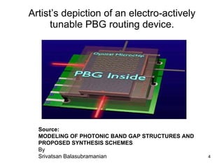
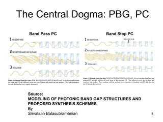
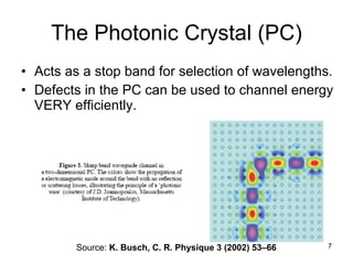
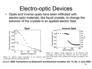
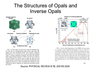
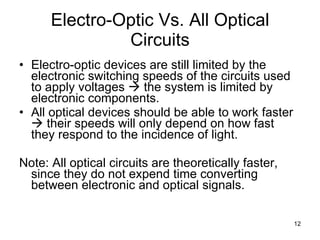
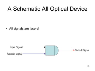
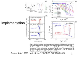
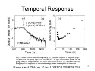
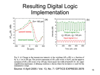
All Optical Circuits and for Digital Logic Optical Bistability or Photonic Switching CCNY Course Presentation for: Introduction to Lasers, under Professor Dorsinville Mohammad Faisal Halim (aka Faissal) Department of Electrical Engineering The City College of New York, CUNY Monday, 14 th  May, 2007
Background All current digital logic circuits are based on the use of electricity. As systems get ever miniaturized electronic systems run into problems with heat and quantum effects. There are inherent limitations to the speed of electrons moving in solids.
Possible Avenue for Extending Moore’s Law: Turn to LIGHT Speed of light in dielectrics is greater than the speed of electrons in conductors and semiconductors. Optical switching speeds are (theoretically, and practically) in excess of electrical switching speeds. Optical switching speeds have very low power consumption (calculated, and demonstrated). Using visible wavelengths, optical devices can be made that are smaller than their semiconductor counterparts.
Artist’s depiction of an electro-actively tunable PBG routing device. Source: MODELING OF PHOTONIC BAND GAP STRUCTURES AND PROPOSED SYNTHESIS SCHEMES By Srivatsan Balasubramanian
Band Pass PC Band Stop PC Source: MODELING OF PHOTONIC BAND GAP STRUCTURES AND PROPOSED SYNTHESIS SCHEMES By Srivatsan Balasubramanian The Central Dogma: PBG, PC
More PC Theory Source: MODELING OF PHOTONIC BAND GAP STRUCTURES AND PROPOSED SYNTHESIS SCHEMES By Srivatsan Balasubramanian
The Photonic Crystal (PC) Acts as a stop band for selection of wavelengths. Defects in the PC can be used to channel energy VERY efficiently. Source:  K. Busch, C. R. Physique 3 (2002) 53–66
Active Digital Devices Do more than just channel light: manipulate it! Two possible switching methods: Electro-optic devices Light modulated devices, utilizing NLO effects or Intensity dependent indices of refraction
Optical Switching: PC Tunability To switch is to change the wavelength that the photonic crystal will let through or reflect.
Electro-optic Devices Opals and inverse opals have been infiltrated with electro-optic materials, like liquid crystals, to change the behavior of the crystals in an applied electric field. Source:  IEEE Transactions on Dielectrics and Electrical Insulation Vol. 13, No. 3; June 2006 Opal Inverse Opal
The Structures of Opals and Inverse Opals Source: PHYSICAL REVIEW B  72 , 205109 2005
Electro-Optic Vs. All Optical Circuits Electro-optic devices are still limited by the electronic switching speeds of the circuits used to apply voltages    the system is limited by electronic components. All optical devices should be able to work faster    their speeds will only depend on how fast they respond to the incidence of light. Note: All optical circuits are theoretically faster, since they do not expend time converting between electronic and optical signals.
A Schematic All Optical Device All signals are lasers! Control Signal Input Signal Output Signal
Implementation Source: 4 April 2005 / Vol. 13, No. 7 / OPTICS EXPRESS 2678
Temporal Response Source: 4 April 2005 / Vol. 13, No. 7 / OPTICS EXPRESS 2678
Resulting Digital Logic Implementation Source: 4 April 2005 / Vol. 13, No. 7 / OPTICS EXPRESS 2678
Fabrication: Why nanostructures? Potential for extremely small devices (visible wavelengths are very small) Potential for large scale self assembly fabrication procedures Potential for large scale chemical synthesis (e.g.: opals and inverse opals)
Why Silicon? Silicon fabrication technology is very mature, and if adapted for all optical circuits then the technology can be brought to market quickly. (Intel claims to have already made an optical chip, so this pressure is probably greater now than a few months ago).
Other PC Technologies not mentioned earlier Quantum dot based opal and inverse opal PCs.
Other Work in the Area All optical ICs, connecting the devices, and optical interconnects.
Future Work Devise more practical fabrication methods Fabricate devices that use visible wavelengths (most current devices use IR, which can result in rather large devices). Devise methods to use the lasing potential of microcavities for use as laser sources, for the transmission of information. Better integration with silicon technology (work on this front is still relatively new).

All optical circuits and for digital logic

  • 1.
    All Optical Circuitsand for Digital Logic Optical Bistability or Photonic Switching CCNY Course Presentation for: Introduction to Lasers, under Professor Dorsinville Mohammad Faisal Halim (aka Faissal) Department of Electrical Engineering The City College of New York, CUNY Monday, 14 th May, 2007
  • 2.
    Background All currentdigital logic circuits are based on the use of electricity. As systems get ever miniaturized electronic systems run into problems with heat and quantum effects. There are inherent limitations to the speed of electrons moving in solids.
  • 3.
    Possible Avenue forExtending Moore’s Law: Turn to LIGHT Speed of light in dielectrics is greater than the speed of electrons in conductors and semiconductors. Optical switching speeds are (theoretically, and practically) in excess of electrical switching speeds. Optical switching speeds have very low power consumption (calculated, and demonstrated). Using visible wavelengths, optical devices can be made that are smaller than their semiconductor counterparts.
  • 4.
    Artist’s depiction ofan electro-actively tunable PBG routing device. Source: MODELING OF PHOTONIC BAND GAP STRUCTURES AND PROPOSED SYNTHESIS SCHEMES By Srivatsan Balasubramanian
  • 5.
    Band Pass PCBand Stop PC Source: MODELING OF PHOTONIC BAND GAP STRUCTURES AND PROPOSED SYNTHESIS SCHEMES By Srivatsan Balasubramanian The Central Dogma: PBG, PC
  • 6.
    More PC TheorySource: MODELING OF PHOTONIC BAND GAP STRUCTURES AND PROPOSED SYNTHESIS SCHEMES By Srivatsan Balasubramanian
  • 7.
    The Photonic Crystal(PC) Acts as a stop band for selection of wavelengths. Defects in the PC can be used to channel energy VERY efficiently. Source: K. Busch, C. R. Physique 3 (2002) 53–66
  • 8.
    Active Digital DevicesDo more than just channel light: manipulate it! Two possible switching methods: Electro-optic devices Light modulated devices, utilizing NLO effects or Intensity dependent indices of refraction
  • 9.
    Optical Switching: PCTunability To switch is to change the wavelength that the photonic crystal will let through or reflect.
  • 10.
    Electro-optic Devices Opalsand inverse opals have been infiltrated with electro-optic materials, like liquid crystals, to change the behavior of the crystals in an applied electric field. Source: IEEE Transactions on Dielectrics and Electrical Insulation Vol. 13, No. 3; June 2006 Opal Inverse Opal
  • 11.
    The Structures ofOpals and Inverse Opals Source: PHYSICAL REVIEW B 72 , 205109 2005
  • 12.
    Electro-Optic Vs. AllOptical Circuits Electro-optic devices are still limited by the electronic switching speeds of the circuits used to apply voltages  the system is limited by electronic components. All optical devices should be able to work faster  their speeds will only depend on how fast they respond to the incidence of light. Note: All optical circuits are theoretically faster, since they do not expend time converting between electronic and optical signals.
  • 13.
    A Schematic AllOptical Device All signals are lasers! Control Signal Input Signal Output Signal
  • 14.
    Implementation Source: 4April 2005 / Vol. 13, No. 7 / OPTICS EXPRESS 2678
  • 15.
    Temporal Response Source:4 April 2005 / Vol. 13, No. 7 / OPTICS EXPRESS 2678
  • 16.
    Resulting Digital LogicImplementation Source: 4 April 2005 / Vol. 13, No. 7 / OPTICS EXPRESS 2678
  • 17.
    Fabrication: Why nanostructures?Potential for extremely small devices (visible wavelengths are very small) Potential for large scale self assembly fabrication procedures Potential for large scale chemical synthesis (e.g.: opals and inverse opals)
  • 18.
    Why Silicon? Siliconfabrication technology is very mature, and if adapted for all optical circuits then the technology can be brought to market quickly. (Intel claims to have already made an optical chip, so this pressure is probably greater now than a few months ago).
  • 19.
    Other PC Technologiesnot mentioned earlier Quantum dot based opal and inverse opal PCs.
  • 20.
    Other Work inthe Area All optical ICs, connecting the devices, and optical interconnects.
  • 21.
    Future Work Devisemore practical fabrication methods Fabricate devices that use visible wavelengths (most current devices use IR, which can result in rather large devices). Devise methods to use the lasing potential of microcavities for use as laser sources, for the transmission of information. Better integration with silicon technology (work on this front is still relatively new).