![Bistable Digital Logic Devices Halim
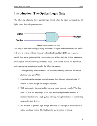
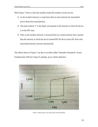
For a device, as depicted in Figure 4, an input (called “Signal” in Figure 4) could come in
at an input intensity slightly less than I1(in) (from Figure 8), and the control signal
(“Control,” from Figure 4) could have an intensity such that the total intensity of the two
beams is slightly greater than I2(in) (from Figure 8), and the resulting output signal
(“Output”, from Figure 4) could be the output from an AND gate, as used in digital logic.
In principle, this sort of bistability is achieved by a saturable absorber. As the incident
intensity is increased, the beam is absorbed by the absorber, until at a certain intensity
[I1(in) (from Figure 8)] the absorber is bleached, ad so it suddenly lets the light through,
with very little loss in intensity. When the incident laser is being reduced in intensity then
the absorber will still have some stored photons, causing it to stay bleached until the
incident beam is reduced in intensity to I2(in) (from Figure 8) – this is lower than I1,
when the absorber looses its stored photons and the transmitted intensity goes down.
Since I2(in) is less than I1(in) (both, from Figure 8) we see the hysteresis.
11](https://image.slidesharecdn.com/allopticalcircuitsandfordigitallogic-101213022642-phpapp01/85/All-optical-circuits-and-for-digital-logic-11-320.jpg)

The document discusses bistable digital logic devices for all optical circuits. It begins with background on how optical architectures could replace electrical ones to overcome limitations of Moore's Law. It then introduces an optical logic gate scheme using a photonic resonant tunneling device based on a photonic crystal nanocavity. This device exhibits single wavelength bistability due to saturable absorption, which could be used to implement digital logic gates. The document also discusses two wavelength bistable switching and concludes that while optical devices are not yet as fast as electronic ones, emerging photonic crystal technologies may enable faster and more efficient all optical computing.