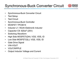
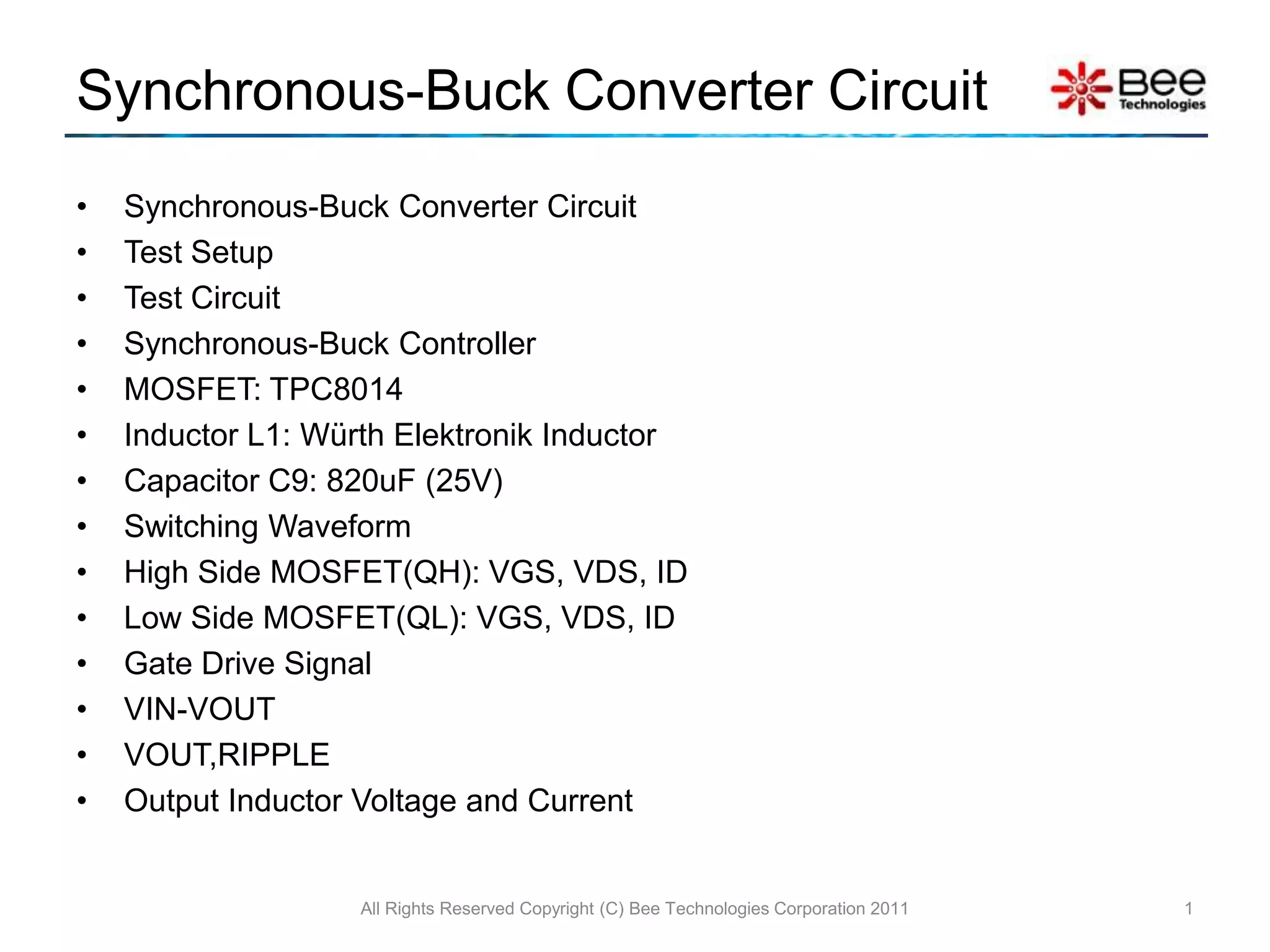
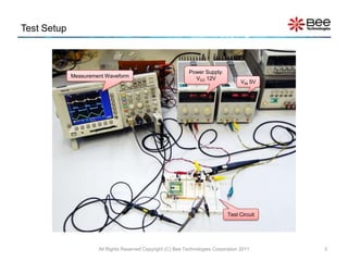
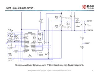
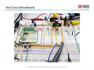
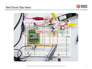
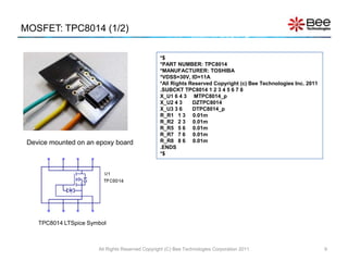
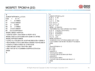
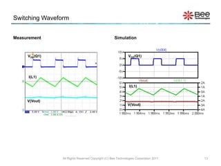
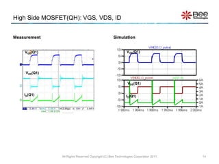
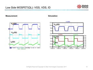
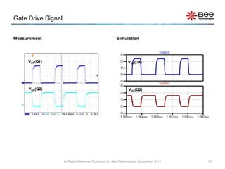
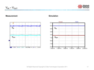
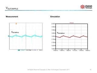
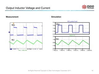
Synchronous-Buck Converter Circuit
•   Synchronous-Buck Converter Circuit
•   Test Setup
•   Test Circuit
•   Synchronous-Buck Controller
•   MOSFET: TPC8014
•   Inductor L1: Würth Elektronik Inductor
•   Capacitor C9: 820uF (25V)
•   Switching Waveform
•   High Side MOSFET(QH): VGS, VDS, ID
•   Low Side MOSFET(QL): VGS, VDS, ID
•   Gate Drive Signal
•   VIN-VOUT
•   VOUT,RIPPLE
•   Output Inductor Voltage and Current


                   All Rights Reserved Copyright (C) Bee Technologies Corporation 2011   1
Synchronous-Buck Converter Circuit


 Duty Cycle (D)
  ≈ Vin/Vout,
   D = 0.368


                  All Rights Reserved Copyright (C) Bee Technologies Corporation 2011   2
Test Setup


                                                              Power Supply:
             Measurement Waveform                               VCC 12V
                                                                                     VIN 5V


                                                                               Test Circuit


                      All Rights Reserved Copyright (C) Bee Technologies Corporation 2011     3
Test Circuit Schematic


       Synchronous-Buck Converter using TPS5618 controller from Texas Instruments

                    All Rights Reserved Copyright (C) Bee Technologies Corporation 2011   4
Test Circuit (Breadboard)


                                                                    Q1


                                                                         Q2


                                Controller


                  All Rights Reserved Copyright (C) Bee Technologies Corporation 2011   5
Test Circuit (Top View)


                                                     L1


                                                                        C9

                                                                                    C10


                                   Controller


                  All Rights Reserved Copyright (C) Bee Technologies Corporation 2011     6
Synchronous-Buck Controller (1/2)

Synchronous-Buck Controller Circuit with IC                  Synchronous-Buck Controller Block Model
TPS5618 from Texas Instruments                               (Open Loop Setting)


                             HIDR
                                                                                               High side gate driver


                                                                                               Low side gate driver
                             LODR


•   The Syn-Buck_Ctrl is a block model that generates gate drive pulse signal to control MOSFET
    switches of the Synchronous-Buck Converter. The duty cycle, switching frequency, and the
    switching dead-time are input into the model to match the real circuit.


                         All Rights Reserved Copyright (C) Bee Technologies Corporation 2011                           7
Synchronous-Buck Controller (2/2)

                                                                                                        Parameters
                                                                                                        •   FREQ = Switching frequency, set to match
                                                                                                            the measurement switching frequency.
     PARAMETERS:                                                                                        •   D = Duty Cycle, calculated by D≈VOUT/VIN
                                                                                                        •
     FREQ = 152kHz
     D = 0.36
                                                                          DHDR1    RHDR1                    tdly = HDR and LDR dead-time, the tdly is
                                   U1                                     Dclmp    0.01
     tdly = 80n                    AND2_ABM                                     N7                          set to match the measurement dead time
               Rdly 1
                        N4
                                                         N5                    N6
                                                                                                  HDR       value.
                                                                          Dclmp RHDR2          CHDR                                      Dead-time, the time
               1k
                             Cdly 1                 VOH = 12              DHDR2 0.01           1n                                         when QH and QL
Pulse                        {tdly /1k}             VOL = 0
                                                                                           0                                                are both off
Control                 0
Signal                                                                                                               1/frequency
                    U5                                             U2
                    INV_ABM                                        AND2_ABM
     N1                                   N2
                                               Rdly 2
                                                        N3                                        LDR
                    VOH = 1.709
                    VOL = 0
                                               1k
          V1                                                 Cdly 2            VOH = 8
                                                             {tdly /1k}        VOL = 0
          TD = {1/FREQ}
          TR = 1n                                       0
          TF = 1n                                                           Dead-time
      0   V1 = 0
          V2 = 1.709                                                        generator
          PW = {D/FREQ}
          PER = {1/FREQ}


      The Syn-Buck_Ctrl Equivalent Circuit


                                                                                                             Gate drive signal (measurement)

                                                                   All Rights Reserved Copyright (C) Bee Technologies Corporation 2011                         8
MOSFET: TPC8014 (1/2)

                                                  *$
                                                  *PART NUMBER: TPC8014
                                                  *MANUFACTURER: TOSHIBA
                                                  *VDSS=30V, ID=11A
                                                  *All Rights Reserved Copyright (c) Bee Technologies Inc. 2011
                                                  .SUBCKT TPC8014 1 2 3 4 5 6 7 8
                                                  X_U1 6 4 3 MTPC8014_p
                                                  X_U2 4 3     DZTPC8014
                                                  X_U3 3 6     DTPC8014_p
                                                  R_R1 1 3 0.01m
                                                  R_R2 2 3 0.01m
                                                  R_R5 5 6 0.01m
                                                  R_R7 7 6 0.01m
 Device mounted on an epoxy board                 R_R8 8 6 0.01m
                                                  .ENDS
                                                  *$


    TPC8014 LTSpice Symbol


                       All Rights Reserved Copyright (C) Bee Technologies Corporation 2011                        9
MOSFET: TPC8014 (2/2)

*$                                                              *$
                                                                .SUBCKT DTPC8014_p A K
.SUBCKT MTPC8014_p D G S
                                                                R_R2 5 6 100
CGD     1    G 1.7n                                             R_R1 3 4 1
R1    1     G 10MEG                                             C_C1 5 6 195p
S1    1 D G D SMOD1                                             E_E1 5 K 3 4 1
                                                                S_S1 6 K 4 K _S1
D1    2     D DGD
                                                                RS_S1 4 K 1G
R2    D     2 10MEG                                             .MODEL _S1 VSWITCH
S2    2 G D G SMOD1                                             + Roff=50MEG Ron=100m Voff=90mV Von=100mV
M1   D G S S MTPC8014                                           G_G1 K A VALUE { V(3,4)-V(5,6) }
                                                                D_D1 2 K DTPC8014
.MODEL SMOD1 VSWITCH
                                                                D_D2 4 K DTPC8014
+ VON=0V VOFF=-10mV RON=1m ROFF=1E12                            F_F1 K 3 VF_F1 1
.MODEL DGD D (CJO=0.950E-9 M=.52396 VJ=.54785)                  VF_F1 A 2 0V
.MODEL MTPC8014 NMOS                                            .MODEL DTPC8014 D
+ LEVEL=3 L=720.00E-9 W=.45 KP=66.000E-6 RS=1.0000E-3           + IS=824.87E-12 N=1.2770 RS=6.2420E-3 IKF=7.3139
                                                                + CJO=3.0000E-12 BV=60 IBV=100.00E-6 TT=24.062E-9
+ RD=6.8436E-3 VTO=2.3063 RDS=3.0000E6 TOX=40.000E-9            .ENDS
+ CGSO=2.7726E-9 CGDO=1E-12 RG=22.95                            *$
+ CBD=342.86E-12 MJ=.70573 PB=.3905                             .subckt DZTPC8014 1 2
+ RB=1 N=5 IS=1E-15 GAMMA=0 KAPPA=0 ETA=0.5m                    D2 1 3 DZ2
                                                                D1 2 3 DZ1
.ENDS
                                                                .model DZ1 D
*$                                                              + IS=0.01p N=0.1 ISR=0
                                                                + CJO=3E-12 BV=22.423 IBV=0.001 RS=0
                                                                .model DZ2 D
                                                                + IS=0.01p N=0.1 ISR=0
                                                                + CJO=3E-12 BV=22.423 IBV=0.001 RS=411.11
                                                                .ENDS
                                                                *$


                            All Rights Reserved Copyright (C) Bee Technologies Corporation 2011                     10
Inductor L1: Würth Elektronik Inductor

                                                                *$
                                                                *PART NUMBER: L7447140
                                                                *MANUFACTURER: Würth Elektronik
                                                                *All Rights Reserved Copyright (c) Bee Technologies Inc. 2011
                                                                .SUBCKT L7447140 1 2
                                                                R_RS 1 N1 10.366m
                                                                L_L1 N1 2 4.84796uH
                                                                C_C1 N1 2 0.357pF
                                                                R_R1 N1 2 15.3375k
                                                                .ENDS
                                                                *$

  Würth Elektronik Inductor part no. 7447140


    LTSpice Symbol


                            All Rights Reserved Copyright (C) Bee Technologies Corporation 2011                          11
Capacitor C9: 820uF (25V)

                                                              *$
                                                              *PART NUMBER: EEUFM1E821L
                                                              *MANUFACTURER: Panasonic
                                                              *CAP=820uF, Vmax=25V
                                                              *All Rights Reserved Copyright (C) Bee Technologies Inc. 2011
                                                              .SUBCKT C820U 1 2
                                                              L_L1 1        N1            8.16935nH
                                                              C_C1          N1            N2            812.73uF
                                                              R_R1          N2            2             15.695m
                                                              .ENDS
                                                               *$

  Capacitor 820uF (25V)


  LTSpice Symbol


                          All Rights Reserved Copyright (C) Bee Technologies Corporation 2011                          12
Switching Waveform


Measurement                                        Simulation


     VDS(Q1)                                                VDS(Q1)


      I(L1)

                                                             I(L1)


     V(Vout)
                                                            V(Vout)


               All Rights Reserved Copyright (C) Bee Technologies Corporation 2011   13
High Side MOSFET(QH): VGS, VDS, ID


Measurement                                        Simulation


    VGS(Q1)                                                 VGS(Q1)


     VDS(Q1)

                                                             VDS(Q1)


    ID(Q1)                                                  ID(Q1)


               All Rights Reserved Copyright (C) Bee Technologies Corporation 2011   14
Low Side MOSFET(QL): VGS, VDS, ID


Measurement                                        Simulation


     VGS(Q2)                                                VGS(Q2)


     VDS(Q2)

                                                           VDS(Q2)


    ID(Q2)                                                  ID(Q2)


               All Rights Reserved Copyright (C) Bee Technologies Corporation 2011   15
Gate Drive Signal


Measurement                                             Simulation


     VGS(Q1)                                                    VGS(Q1)


     VGS(Q2)                                                    VGS(Q2)


                    All Rights Reserved Copyright (C) Bee Technologies Corporation 2011   16
VIN – VOUT


Measurement                                       Simulation


     VIN                                                   VIN


     VOUT                                                   VOUT


              All Rights Reserved Copyright (C) Bee Technologies Corporation 2011   17
VOUT,RIPPLE


Measurement                                            Simulation


     VOUT,RIPPLE                                                  VOUT,RIPPLE


                   All Rights Reserved Copyright (C) Bee Technologies Corporation 2011   18
Output Inductor Voltage and Current


Measurement                                          Simulation


                                                             V(L)
     V(L)


                                                             I(L)
     I(L)


                 All Rights Reserved Copyright (C) Bee Technologies Corporation 2011   19

Synchronous Buck Converter using LTspice

  • 1.
    Synchronous-Buck Converter Circuit • Synchronous-Buck Converter Circuit • Test Setup • Test Circuit • Synchronous-Buck Controller • MOSFET: TPC8014 • Inductor L1: Würth Elektronik Inductor • Capacitor C9: 820uF (25V) • Switching Waveform • High Side MOSFET(QH): VGS, VDS, ID • Low Side MOSFET(QL): VGS, VDS, ID • Gate Drive Signal • VIN-VOUT • VOUT,RIPPLE • Output Inductor Voltage and Current All Rights Reserved Copyright (C) Bee Technologies Corporation 2011 1
  • 2.
    Synchronous-Buck Converter Circuit Duty Cycle (D) ≈ Vin/Vout, D = 0.368 All Rights Reserved Copyright (C) Bee Technologies Corporation 2011 2
  • 3.
    Test Setup Power Supply: Measurement Waveform VCC 12V VIN 5V Test Circuit All Rights Reserved Copyright (C) Bee Technologies Corporation 2011 3
  • 4.
    Test Circuit Schematic Synchronous-Buck Converter using TPS5618 controller from Texas Instruments All Rights Reserved Copyright (C) Bee Technologies Corporation 2011 4
  • 5.
    Test Circuit (Breadboard) Q1 Q2 Controller All Rights Reserved Copyright (C) Bee Technologies Corporation 2011 5
  • 6.
    Test Circuit (TopView) L1 C9 C10 Controller All Rights Reserved Copyright (C) Bee Technologies Corporation 2011 6
  • 7.
    Synchronous-Buck Controller (1/2) Synchronous-BuckController Circuit with IC Synchronous-Buck Controller Block Model TPS5618 from Texas Instruments (Open Loop Setting) HIDR High side gate driver Low side gate driver LODR • The Syn-Buck_Ctrl is a block model that generates gate drive pulse signal to control MOSFET switches of the Synchronous-Buck Converter. The duty cycle, switching frequency, and the switching dead-time are input into the model to match the real circuit. All Rights Reserved Copyright (C) Bee Technologies Corporation 2011 7
  • 8.
    Synchronous-Buck Controller (2/2) Parameters • FREQ = Switching frequency, set to match the measurement switching frequency. PARAMETERS: • D = Duty Cycle, calculated by D≈VOUT/VIN • FREQ = 152kHz D = 0.36 DHDR1 RHDR1 tdly = HDR and LDR dead-time, the tdly is U1 Dclmp 0.01 tdly = 80n AND2_ABM N7 set to match the measurement dead time Rdly 1 N4 N5 N6 HDR value. Dclmp RHDR2 CHDR Dead-time, the time 1k Cdly 1 VOH = 12 DHDR2 0.01 1n when QH and QL Pulse {tdly /1k} VOL = 0 0 are both off Control 0 Signal 1/frequency U5 U2 INV_ABM AND2_ABM N1 N2 Rdly 2 N3 LDR VOH = 1.709 VOL = 0 1k V1 Cdly 2 VOH = 8 {tdly /1k} VOL = 0 TD = {1/FREQ} TR = 1n 0 TF = 1n Dead-time 0 V1 = 0 V2 = 1.709 generator PW = {D/FREQ} PER = {1/FREQ} The Syn-Buck_Ctrl Equivalent Circuit Gate drive signal (measurement) All Rights Reserved Copyright (C) Bee Technologies Corporation 2011 8
  • 9.
    MOSFET: TPC8014 (1/2) *$ *PART NUMBER: TPC8014 *MANUFACTURER: TOSHIBA *VDSS=30V, ID=11A *All Rights Reserved Copyright (c) Bee Technologies Inc. 2011 .SUBCKT TPC8014 1 2 3 4 5 6 7 8 X_U1 6 4 3 MTPC8014_p X_U2 4 3 DZTPC8014 X_U3 3 6 DTPC8014_p R_R1 1 3 0.01m R_R2 2 3 0.01m R_R5 5 6 0.01m R_R7 7 6 0.01m Device mounted on an epoxy board R_R8 8 6 0.01m .ENDS *$ TPC8014 LTSpice Symbol All Rights Reserved Copyright (C) Bee Technologies Corporation 2011 9
  • 10.
    MOSFET: TPC8014 (2/2) *$ *$ .SUBCKT DTPC8014_p A K .SUBCKT MTPC8014_p D G S R_R2 5 6 100 CGD 1 G 1.7n R_R1 3 4 1 R1 1 G 10MEG C_C1 5 6 195p S1 1 D G D SMOD1 E_E1 5 K 3 4 1 S_S1 6 K 4 K _S1 D1 2 D DGD RS_S1 4 K 1G R2 D 2 10MEG .MODEL _S1 VSWITCH S2 2 G D G SMOD1 + Roff=50MEG Ron=100m Voff=90mV Von=100mV M1 D G S S MTPC8014 G_G1 K A VALUE { V(3,4)-V(5,6) } D_D1 2 K DTPC8014 .MODEL SMOD1 VSWITCH D_D2 4 K DTPC8014 + VON=0V VOFF=-10mV RON=1m ROFF=1E12 F_F1 K 3 VF_F1 1 .MODEL DGD D (CJO=0.950E-9 M=.52396 VJ=.54785) VF_F1 A 2 0V .MODEL MTPC8014 NMOS .MODEL DTPC8014 D + LEVEL=3 L=720.00E-9 W=.45 KP=66.000E-6 RS=1.0000E-3 + IS=824.87E-12 N=1.2770 RS=6.2420E-3 IKF=7.3139 + CJO=3.0000E-12 BV=60 IBV=100.00E-6 TT=24.062E-9 + RD=6.8436E-3 VTO=2.3063 RDS=3.0000E6 TOX=40.000E-9 .ENDS + CGSO=2.7726E-9 CGDO=1E-12 RG=22.95 *$ + CBD=342.86E-12 MJ=.70573 PB=.3905 .subckt DZTPC8014 1 2 + RB=1 N=5 IS=1E-15 GAMMA=0 KAPPA=0 ETA=0.5m D2 1 3 DZ2 D1 2 3 DZ1 .ENDS .model DZ1 D *$ + IS=0.01p N=0.1 ISR=0 + CJO=3E-12 BV=22.423 IBV=0.001 RS=0 .model DZ2 D + IS=0.01p N=0.1 ISR=0 + CJO=3E-12 BV=22.423 IBV=0.001 RS=411.11 .ENDS *$ All Rights Reserved Copyright (C) Bee Technologies Corporation 2011 10
  • 11.
    Inductor L1: WürthElektronik Inductor *$ *PART NUMBER: L7447140 *MANUFACTURER: Würth Elektronik *All Rights Reserved Copyright (c) Bee Technologies Inc. 2011 .SUBCKT L7447140 1 2 R_RS 1 N1 10.366m L_L1 N1 2 4.84796uH C_C1 N1 2 0.357pF R_R1 N1 2 15.3375k .ENDS *$ Würth Elektronik Inductor part no. 7447140 LTSpice Symbol All Rights Reserved Copyright (C) Bee Technologies Corporation 2011 11
  • 12.
    Capacitor C9: 820uF(25V) *$ *PART NUMBER: EEUFM1E821L *MANUFACTURER: Panasonic *CAP=820uF, Vmax=25V *All Rights Reserved Copyright (C) Bee Technologies Inc. 2011 .SUBCKT C820U 1 2 L_L1 1 N1 8.16935nH C_C1 N1 N2 812.73uF R_R1 N2 2 15.695m .ENDS *$ Capacitor 820uF (25V) LTSpice Symbol All Rights Reserved Copyright (C) Bee Technologies Corporation 2011 12
  • 13.
    Switching Waveform Measurement Simulation VDS(Q1) VDS(Q1) I(L1) I(L1) V(Vout) V(Vout) All Rights Reserved Copyright (C) Bee Technologies Corporation 2011 13
  • 14.
    High Side MOSFET(QH):VGS, VDS, ID Measurement Simulation VGS(Q1) VGS(Q1) VDS(Q1) VDS(Q1) ID(Q1) ID(Q1) All Rights Reserved Copyright (C) Bee Technologies Corporation 2011 14
  • 15.
    Low Side MOSFET(QL):VGS, VDS, ID Measurement Simulation VGS(Q2) VGS(Q2) VDS(Q2) VDS(Q2) ID(Q2) ID(Q2) All Rights Reserved Copyright (C) Bee Technologies Corporation 2011 15
  • 16.
    Gate Drive Signal Measurement Simulation VGS(Q1) VGS(Q1) VGS(Q2) VGS(Q2) All Rights Reserved Copyright (C) Bee Technologies Corporation 2011 16
  • 17.
    VIN – VOUT Measurement Simulation VIN VIN VOUT VOUT All Rights Reserved Copyright (C) Bee Technologies Corporation 2011 17
  • 18.
    VOUT,RIPPLE Measurement Simulation VOUT,RIPPLE VOUT,RIPPLE All Rights Reserved Copyright (C) Bee Technologies Corporation 2011 18
  • 19.
    Output Inductor Voltageand Current Measurement Simulation V(L) V(L) I(L) I(L) All Rights Reserved Copyright (C) Bee Technologies Corporation 2011 19