A microprocessor is an electronic component that is used by a computer to do its work. It is a central processing unit on a single integrated circuit chip containing millions of very small components including transistors, resistors, and diodes that work together.
Machine Language Instruction Formats – Instruction Set of 8086-Data transfer
instructions,Arithmetic and Logic instructions,Branch instructions,Loop instructions,Processor
Control instructions,Flag Manipulation instructions,Shift and Rotate instructions,String
instructions, Assembler Directives and operators,Example Programs,Introduction to Stack,
STACK Structure of 8086, Interrupts and Interrupt Service Routines, Interrupt Cycle of 8086,
Non-Maskable and Maskable Interrupts, Interrupt Programming, MACROS.
MPMC UNIT-1. Microprocessor 8085 pdf Microprocessor and MicrocontrollerRAHUL RANJAN
Diploma in Electrical Engineering MICROPROCESSOR AND MICROCONTROLLER UNIT-1 Full Notes 📝 Microprocessor 8085 State Board Of Technical Education [SBTE] BIHAR
A microprocessor is an electronic component that is used by a computer to do its work. It is a central processing unit on a single integrated circuit chip containing millions of very small components including transistors, resistors, and diodes that work together. Some microprocessors in the 20th century required several chips. Microprocessors help to do everything from controlling elevators to searching the Web. Everything a computer does is described by instructions of computer programs, and microprocessors carry out these instructions many millions of times a second. [1]
Microprocessors were invented in the 1970s for use in embedded systems. The majority are still used that way, in such things as mobile phones, cars, military weapons, and home appliances. Some microprocessors are microcontrollers, so small and inexpensive that they are used to control very simple products like flashlights and greeting cards that play music when you open them. A few especially powerful microprocessors are used in personal computers.
To understand the basic concepts of 8085 microprocessor, microcontroller. The students will also learn about the programming methods and integration of peripherals to the micro-controller.
ccfghlm,,fghggjjghkgkjkjkjklhljhlkjhljhlhjl
bnjkhhkbkbn,mn,mn,mn,mn,mn,mn,m,mn,bn,bn,mbn,bj,bjbj,bjbj,bm, dvglksmndgopjpjmlkvmsodfgjhonjhlkmnlkmdvokji0fpqokdf[k[akfmcadokjvojisdlkmlkswopdvgopko;pmfasd f
\plvsf[prblpk[bnpk
A microprocessor is an electronic component that is used by a computer to do its work. It is a central processing unit on a single integrated circuit chip containing millions of very small components including transistors, resistors, and diodes that work together. Some microprocessors in the 20th century required several chips. Microprocessors help to do everything from controlling elevators to searching the Web. Everything a computer does is described by instructions of computer programs, and microprocessors carry out these instructions many millions of times a second. [1]
Microprocessors were invented in the 1970s for use in embedded systems. The majority are still used that way, in such things as mobile phones, cars, military weapons, and home appliances. Some microprocessors are microcontrollers, so small and inexpensive that they are used to control very simple products like flashlights and greeting cards that play music when you open them. A few especially powerful microprocessors are used in personal computers.
Chances are you have a Wi-Fi network at home, or live close to one (or more) that tantalizingly pops up in a list whenever you boot up the laptop.
The problem is, if there's a lock next to the network name (AKA the SSID, or service set identifier), that indicates security is activated. Without the password or passphrase, you're not going to get access to that network, or the sweet, sweet internet that goes with it.
A distributed denial-of-service (DDoS) attack is a malicious attempt to disrupt normal traffic of a targeted server, service or network by overwhelming the target or its surrounding infrastructure with a flood of Internet traffic. DDoS attacks achieve effectiveness by utilizing multiple compromised computer systems as sources of attack traffic. Exploited machines can include computers and other networked resources such as IoT devices. From a high level, a DDoS attack is like a traffic jam clogging up with highway, preventing regular traffic from arriving at its desired destination.
A microprocessor is an electronic component that is used by a computer to do its work. It is a central processing unit on a single integrated circuit chip containing millions of very small components including transistors, resistors, and diodes that work together.
A microprocessor is an electronic component that is used by a computer to do its work. It is a central processing unit on a single integrated circuit chip containing millions of very small components including transistors, resistors, and diodes that work together.
A microprocessor is an electronic component that is used by a computer to do its work. It is a central processing unit on a single integrated circuit chip containing millions of very small components including transistors, resistors, and diodes that work together.
A microprocessor is an electronic component that is used by a computer to do its work. It is a central processing unit on a single integrated circuit chip containing millions of very small components including transistors, resistors, and diodes that work together.
A microprocessor is an electronic component that is used by a computer to do its work. It is a central processing unit on a single integrated circuit chip containing millions of very small components including transistors, resistors, and diodes that work together.
A microprocessor is an electronic component that is used by a computer to do its work. It is a central processing unit on a single integrated circuit chip containing millions of very small components including transistors, resistors, and diodes that work together.
A microprocessor is an electronic component that is used by a computer to do its work. It is a central processing unit on a single integrated circuit chip containing millions of very small components including transistors, resistors, and diodes that work together.
A microprocessor is an electronic component that is used by a computer to do its work. It is a central processing unit on a single integrated circuit chip containing millions of very small components including transistors, resistors, and diodes that work together.
A microprocessor is an electronic component that is used by a computer to do its work. It is a central processing unit on a single integrated circuit chip containing millions of very small components including transistors, resistors, and diodes that work together. Some microprocessors in the 20th century required several chips. Microprocessors help to do everything from controlling elevators to searching the Web. Everything a computer does is described by instructions of computer programs, and microprocessors carry out these instructions many millions of times a second. [1]
Microprocessors were invented in the 1970s for use in embedded systems. The majority are still used that way, in such things as mobile phones, cars, military weapons, and home appliances. Some microprocessors are microcontrollers, so small and inexpensive that they are used to control very simple products like flashlights and greeting cards that play music when you open them. A few especially powerful microprocessors are used in personal computers.
Cosmetic shop management system project report.pdfKamal Acharya
Buying new cosmetic products is difficult. It can even be scary for those who have sensitive skin and are prone to skin trouble. The information needed to alleviate this problem is on the back of each product, but it's thought to interpret those ingredient lists unless you have a background in chemistry.
Instead of buying and hoping for the best, we can use data science to help us predict which products may be good fits for us. It includes various function programs to do the above mentioned tasks.
Data file handling has been effectively used in the program.
The automated cosmetic shop management system should deal with the automation of general workflow and administration process of the shop. The main processes of the system focus on customer's request where the system is able to search the most appropriate products and deliver it to the customers. It should help the employees to quickly identify the list of cosmetic product that have reached the minimum quantity and also keep a track of expired date for each cosmetic product. It should help the employees to find the rack number in which the product is placed.It is also Faster and more efficient way.
CFD Simulation of By-pass Flow in a HRSG module by R&R Consult.pptxR&R Consult
CFD analysis is incredibly effective at solving mysteries and improving the performance of complex systems!
Here's a great example: At a large natural gas-fired power plant, where they use waste heat to generate steam and energy, they were puzzled that their boiler wasn't producing as much steam as expected.
R&R and Tetra Engineering Group Inc. were asked to solve the issue with reduced steam production.
An inspection had shown that a significant amount of hot flue gas was bypassing the boiler tubes, where the heat was supposed to be transferred.
R&R Consult conducted a CFD analysis, which revealed that 6.3% of the flue gas was bypassing the boiler tubes without transferring heat. The analysis also showed that the flue gas was instead being directed along the sides of the boiler and between the modules that were supposed to capture the heat. This was the cause of the reduced performance.
Based on our results, Tetra Engineering installed covering plates to reduce the bypass flow. This improved the boiler's performance and increased electricity production.
It is always satisfying when we can help solve complex challenges like this. Do your systems also need a check-up or optimization? Give us a call!
Work done in cooperation with James Malloy and David Moelling from Tetra Engineering.
More examples of our work https://www.r-r-consult.dk/en/cases-en/
Water scarcity is the lack of fresh water resources to meet the standard water demand. There are two type of water scarcity. One is physical. The other is economic water scarcity.
Explore the innovative world of trenchless pipe repair with our comprehensive guide, "The Benefits and Techniques of Trenchless Pipe Repair." This document delves into the modern methods of repairing underground pipes without the need for extensive excavation, highlighting the numerous advantages and the latest techniques used in the industry.
Learn about the cost savings, reduced environmental impact, and minimal disruption associated with trenchless technology. Discover detailed explanations of popular techniques such as pipe bursting, cured-in-place pipe (CIPP) lining, and directional drilling. Understand how these methods can be applied to various types of infrastructure, from residential plumbing to large-scale municipal systems.
Ideal for homeowners, contractors, engineers, and anyone interested in modern plumbing solutions, this guide provides valuable insights into why trenchless pipe repair is becoming the preferred choice for pipe rehabilitation. Stay informed about the latest advancements and best practices in the field.
Vaccine management system project report documentation..pdfKamal Acharya
The Division of Vaccine and Immunization is facing increasing difficulty monitoring vaccines and other commodities distribution once they have been distributed from the national stores. With the introduction of new vaccines, more challenges have been anticipated with this additions posing serious threat to the already over strained vaccine supply chain system in Kenya.
Immunizing Image Classifiers Against Localized Adversary Attacksgerogepatton
This paper addresses the vulnerability of deep learning models, particularly convolutional neural networks
(CNN)s, to adversarial attacks and presents a proactive training technique designed to counter them. We
introduce a novel volumization algorithm, which transforms 2D images into 3D volumetric representations.
When combined with 3D convolution and deep curriculum learning optimization (CLO), itsignificantly improves
the immunity of models against localized universal attacks by up to 40%. We evaluate our proposed approach
using contemporary CNN architectures and the modified Canadian Institute for Advanced Research (CIFAR-10
and CIFAR-100) and ImageNet Large Scale Visual Recognition Challenge (ILSVRC12) datasets, showcasing
accuracy improvements over previous techniques. The results indicate that the combination of the volumetric
input and curriculum learning holds significant promise for mitigating adversarial attacks without necessitating
adversary training.
TECHNICAL TRAINING MANUAL GENERAL FAMILIARIZATION COURSEDuvanRamosGarzon1
AIRCRAFT GENERAL
The Single Aisle is the most advanced family aircraft in service today, with fly-by-wire flight controls.
The A318, A319, A320 and A321 are twin-engine subsonic medium range aircraft.
The family offers a choice of engines
COLLEGE BUS MANAGEMENT SYSTEM PROJECT REPORT.pdfKamal Acharya
The College Bus Management system is completely developed by Visual Basic .NET Version. The application is connect with most secured database language MS SQL Server. The application is develop by using best combination of front-end and back-end languages. The application is totally design like flat user interface. This flat user interface is more attractive user interface in 2017. The application is gives more important to the system functionality. The application is to manage the student’s details, driver’s details, bus details, bus route details, bus fees details and more. The application has only one unit for admin. The admin can manage the entire application. The admin can login into the application by using username and password of the admin. The application is develop for big and small colleges. It is more user friendly for non-computer person. Even they can easily learn how to manage the application within hours. The application is more secure by the admin. The system will give an effective output for the VB.Net and SQL Server given as input to the system. The compiled java program given as input to the system, after scanning the program will generate different reports. The application generates the report for users. The admin can view and download the report of the data. The application deliver the excel format reports. Because, excel formatted reports is very easy to understand the income and expense of the college bus. This application is mainly develop for windows operating system users. In 2017, 73% of people enterprises are using windows operating system. So the application will easily install for all the windows operating system users. The application-developed size is very low. The application consumes very low space in disk. Therefore, the user can allocate very minimum local disk space for this application.
Quality defects in TMT Bars, Possible causes and Potential Solutions.PrashantGoswami42
Maintaining high-quality standards in the production of TMT bars is crucial for ensuring structural integrity in construction. Addressing common defects through careful monitoring, standardized processes, and advanced technology can significantly improve the quality of TMT bars. Continuous training and adherence to quality control measures will also play a pivotal role in minimizing these defects.
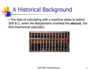
1. BLM 3622- Microprocessors 1
A Historical Background
• The idea of calculating with a machine dates to before
500 B.C. when the Babylonians invented the abacus, the
first mechanical calculator.
2. BLM 3622- Microprocessors 2
Blaise Pascal (1623-1662)
The abacus was not improved until 1642, when
Blaise Pascal invented a calculator constructed a
gear and wheels.
3. BLM 3622- Microprocessors 3
Charles Babbage
One early pioneer of mechanical computing machinery was
Charles Babbage and produce a programmable calculating
machine in 1823. He create the “Analytical Engine”. This machine
was a mechanical computer that stored 1000 20-digit decimal
numbers and variable program that could modify the function of the
machine.
4. BLM 3622- Microprocessors 4
In 1889, Herman Hollerith developed the punched card for
storing data and also developed a mechanical machine-driven
by one of the new electric motors. He was the former of IBM
Corporation.
Herman Hollerith
5. BLM 3622- Microprocessors 5
Konrad Zuse
The first electronic calculating machine invented in
1941 by Konrad Zuse. He had released the first
programmable computer designed to solve
complex engineering equations. It was also the first
machine to work on the binary system, as opposed
to the more familiar decimal system. His calculating
computer was used in aircraft and missile design
during World War II for the German war effort.
7. BLM 3622- Microprocessors 7
The first truly electronic computer was places into
operation in 1943 to break secret German military
codes. The first electronic computer system, which
used vacuum tubes, was invented by Alan Turing
who is a British mathematician . Turing called this
machine Colossus, most likely because its size. A
problem with Colossus was that although its design
allowed it to break secret German military codes
generated by mechanical Enigma machine, it could
not solve other problems. Colossus was not
programmable- it was a fixed program computer
system.
Alan Turing
9. BLM 3622- Microprocessors 9
The first general purpose
programmable computer
system was developed in
1946 and called ENIAC.
The ENIAC was a huge
machine(30 tons) and
performed about 100 000
operation per second.
ENIAC
10. BLM 3622- Microprocessors 10
John von Neumann
In 1945, Von Neumann
contributed a new
understanding of how
practical fast computers
should be organized and
built; these ideas, often
referred to as the stored-
program technique,
became fundamental for
future generations of
high-speed digital
computers and were
universally adopted.
12. BLM 3622- Microprocessors 12
INTEL 4004
The development of transistor in 1948, followed by
the invention of the integrated circuits in 1958. In
1971, the first microprocessor Intel 4004 was
developed. 4004 was a 4-bit microprocessor and
instruction set contains 45 instruction. It performed
about 50 000 instruction per second.
13. BLM 3622- Microprocessors 13
In 1978, Intel released the 8086 microprocessor
which was 16-bit microprocessor and performed 2.5
million instruction per second.
This microprocessor were called CISC(Complex
Instruction Set Computers) because of the number
and complexity of instructions.
The popularity of Intel family was ensured in 1981
when IBM Corp. decided to use 8088/8086
microprocessors in its personal computers.
Intel 8086
14. BLM 3622- Microprocessors 14
Intel 8086/8088 Microprocessors
Intel 8086 and 8088 Microprocessors are
the basis of all IBM-PC compatible
computers
(8086 introduced in 1978, first IBM-PC released in 1981)
All Intel, AMD and other advanced
microprocessors are based on and are
compatible with the original 8086/8
At Power Up and Reset time, Pentiums,
Athlons etc all look like 8086 processors
15. BLM 3622- Microprocessors 15
Intel 8086/8088 Microprocessors
Intel 8086 is a 16-bit microprocessor
16-bit data registers
16 or 8 bit external data bus
Some techniques to optimise the CPU
performance when it’s executing programs
Segment: Offset memory model
Little-Endian Data Format
16. BLM 3622- Microprocessors 16
8086/8088 (1)
Original IBM PC used 8088 micrprocessor
8088 is similar to the 8086 microprocessor but it
has an external 8-bit bus & only 4-deep queue
For cost reduction reasons
We can consider 8086 and 8088 together
PC clones often used 8086 for better
performance
8-bit bus reduces performance, but meant
cheaper computers
17. BLM 3622- Microprocessors 17
8086/8088 (2)
Remember the Fetch-Decode-Execute cycle?
Fetching from EXTERNAL MEMORY is SLOW
The 8086/8 used an instruction queue to
speed up performance
While the processor is decoding and
executing an instruction, its bus interface
can be reading new instructions, since at
that time the bus is not actually in use
18. BLM 3622- Microprocessors 18
8086/8088 Functional Units
Execution Unit
(EU)
Bus Interface
Unit(BIU)
Fetches Opcodes,
Reads Operands,
Writes Data
8086/8088 MPU
19. BLM 3622- Microprocessors 19
8086/8088 (3)
8086/8088 consists of two internal units
The execution unit (EU) - executes the
instructions
The bus interface unit (BIU) - fetches
instructions, reads operands and writes results
The 8086 has a 6-byte prefetch queue
The 8088 has a 4-byte prefetch queue
20. BLM 3622- Microprocessors 20
8086/8088 Internal Organisation
Temporary
Registers
ALU
Flags
EU
Control
AH AL
BH BL
CH CL
DH DL
SP
BP
DI
BI
CS
DS
SS
ES
IO
Internal
Communications
Registers
SUMMATION
Address Bus 20 bits
Data Bus
Bus
Control
1 2 3 4
Instruction Queue
8088
Bus
EU BIU
21. BIU Elements
Instruction Queue: the next instructions or data can be
fetched from memory while the processor is executing
the current instruction
The memory interface is slower than the processor execution
time so this speeds up overall performance
Segment Registers:
CS, DS, SS and ES are 16-bit registers
Used with the 16-bit Base registers to generate the 20-bit
address
Allow the 8086/8088 to address 1Mb of memory
Changed under program control to point to different segments
as a program executes
Instruction Pointer (IP) contains the Offset Address of
the next instruction, the distance in bytes from the
address given by the current CS register
BLM 3622- Microprocessors 21
24. BLM 3622- Microprocessors 24
Exercise: 20-bit Addressing
1. CS contains 0A820h,IP contains 0CE24h.
What is the resulting physical address?
2. CS contains 0B500h, IP contains 0024h.
What is the resulting physical address?
25. BLM 3622- Microprocessors 25
Segment Registers
The utilization of the segment registers
essentially divides the memory space into
overlapping segments, with each segment
being 64K bytes long and at an address that
is divisible by 16.
26. BLM 3622- Microprocessors 26
The advantage of using segment registers
Allow the memory capacity to be 1 M Byte even
though the addresses associated with the individual
instructions are only 16 bits wide.
Allow the instruction, data or stack portion of a
program to be more than 64K Bytes long by allowing
more than one code, data or stack segment.
Facilitate the use of separate memory areas for a
program, its data and the stack.
Permit a program and/or its data to be put into
different areas of memory each time the program is
executed.
27. BLM 3622- Microprocessors 27
8086/8 In Circuit (1)
8086/8 microprocessors need support
circuits in a microcomputer system
8086/8 multiplex the address and data
buses on the same pins
This saves pins but at a price:
Demultiplexing logic is needed to build up
separate address and data buses to interface
with RAMs and ROMs
29. BLM 3622- Microprocessors 29
Pin Connections
AD15-AD0: (I/O-3)
The 8086 address/data bus lines compose
the upper multiplexed address/data bus on
8086. These lines contains address bits
whenever ALE is logic 1. These pins enter
a high-impedance state whenever a hold
acknowledge occurs.
30. BLM 3622- Microprocessors 30
A19/S6-A16/S3: (O-3)
The address/status bus bits are multiplexed to
provide address signals A19-A16 and also status
bits S6-S3. The pins also attain a high-impedance
state during the hold acknowledge. S4 and S3
show which segment is accessed during the
current bus cycle.
Pin Connections
31. BLM 3622- Microprocessors 31
Pin Connections
S4 S3 Function
0 0 Extra segment
0 1 Stack segment
1 0 Code or no segment
1 1 Data segment
32. BLM 3622- Microprocessors 32
Pin Connections
: (O-3)
Whenever the read signal is logic 0, the data bus
is receptive to data from the memory or I/O
devices connected to system.
READY: (I)
This input is controlled to insert wait states into
the timing of the microprocessor.
READY=0: P enters into wait states and remain idle
READY=1: It has no effect on operation of P
RD
33. BLM 3622- Microprocessors 33
Pin Connections
: (I)
The test pin is an input that is tested by the WAIT
instruction.
NMI: (I)
The non-maskable interrupt input is similar to
INTR except that the NMI does not check to see
if IF flag bit is a logic 1. This interrupt input uses
interrupt vector 2.
TEST
34. BLM 3622- Microprocessors 34
Pin Connections
7/ SBHE
RESET: (I)
The reset input causes the P to reset itself if this pin
is held high for a minimum four clocking periods.
It begins executing instructions at memory location
FFFF0H and disables future interrupts by clearing
the IF flag bit.
: (I)
Minimum/maximum mode pin select.
: (O-3)
BHE pin is used to enable the most sig. data bus
bits (D15-D8) during a read or write operation.
MXMN /
35. BLM 3622- Microprocessors 35
Minimum mode Pins
IOM / : (O-3)
The pin selects memory or I/O. This pin
indicates that the microprocessor address bus
contains either a memory address or an I/O
port address.
: (O-3)
This line indicates that 8086 is outputting data
to a memory or I/O device.
WR
36. BLM 3622- Microprocessors 36
Minimum mode Pins
: (O-3)
The interrupt acknowledge signal is a response to
the INTR input pin. This pin is normally used to
gate the interrupt vector number onto the data
bus in response to an interrupt request.
: (O)
Address latch enable shows that the 8086
address/data bus contains address information.
This address can be a memory address or an
I/O port number.
INTA
ALE
37. BLM 3622- Microprocessors 37
Minimum mode Pins
:(0-3)
The data transmit/receive signal shows that the
microprocessor data bus is transmitting or
receiving data.
: (O-3)
Data bus enable activates external data bus
buffers.
RDT /
DEN
38. BLM 3622- Microprocessors 38
HOLD : (I)
The hold input requests a direct memory access
(DMA). If the HOLD signal is logic 1, the
microprocessor stops executing software and places
its address, data and control bus at the high-
impedance state.
HLDA : (O)
Hold acknowledge indicates that the 8086
microprocessor entered the hold state.
Minimum mode Pins
39. BLM 3622- Microprocessors 39
Maximum mode Pins
In order to achieve maximum mode for use
with external coprocessors or
multiprocessing applications.
(O)
The status bits indicate the function of
the current bus cycle. These signals
are normally decoded by the 8288 bus
controller.
:0and,1,2 SSS
42. BLM 3622- Microprocessors 42
8086/8 In Circuit (2)
In Maximum Mode the 8086/8 needs at
least the following: 8288 Bus Controller,
8284A Clock Generator, 74HC373s and
74HC245s
With the aid of these devices the 8086
begins to look like the ideal
microprocessor we looked at earlier
44. BLM 3622- Microprocessors 44
8086/8 Maximum Mode
In maximum mode, the 8288 uses a set of
status signals (S0, S1, S2) to rebuild the
normal bus control signals of the
microprocessor
MRDC#, MWTC#, IORC#, IOWC# etc
Equivalent to MEMR# etc
Look at some special signals briefly
47. BLM 3622- Microprocessors 47
RESET# Signal
The Active low RESET# signal puts the 8086/8
into a defined state
Clears the flags register, segment registers etc.
Sets the effective program address to 0FFFF0h
(CS=0F000h, IP=0FFF0h)
8086/8 Programs always start at FFFF0H after
Reset has been asserted and removed
Continues into latest generation CPUs
48. BLM 3622- Microprocessors 48
BHE# Signal (8086 Only)
The 8086 processor can address memory a
byte at a time
Its data bus is 16-bits wide
It uses the BHE# signal and A0 (sometimes
called BLE#) to address bytes using its 16-
bit bus
50. BLM 3622- Microprocessors 50
Use of BHE#/BLE#
BHE# A0/BLE# Selection
0 0 Whole word (16-bits)
0 1 High byte to/from odd
address
1 0 Low byte to/from even
address
1 1 No selection
51. BLM 3622- Microprocessors 51
ALE and Address/data Bus
Multiplexing
8086/8 Multiplexes the Address and Data
signals onto the same set of pins
Need off-chip logic to separate the signals
Transparent latches designed just for
address demultiplexing
52. BLM 3622- Microprocessors 52
ALE and 74HC373 Transparent Latch
Address
Time
Clock
Address/
Data
Bus
Data Time
ALE
Output of
74HC373
Microcomputer AddressBus
LE
OE#
ALE
Address/
Data Bus
System Address Bus
In0:In7 Q0:Q7
74HC373 or equivalent
TriState Control signal,
OE#, shown connected to
GND for simplicity
53. BLM 3622- Microprocessors 53
Use of ALE (Address Latch Enable)
ALE is used with an external latch
(74HC373) to demultiplex the address and
data lines
74HC373 is transparent when its LE input
(connected to ALE) is high
When ALE goes low, the ‘373 holds the last
data until ALE goes high again
54. BLM 3622- Microprocessors 54
8288 Bus Controller and Bus
Transceivers
8288
Bus Controller
DIR
DEN#
DT/R#
74HC245
EN#
74HC245
EN#
DIR
DIR
CPU [D15:D8]
CPU [D7:D0]
Buffered [D15:D8]
Buffered [D7:D0]
ToMemoryandI/O
Systems
8288 Bus Controller also
generates Direction and
Enable signals for Bi-
Directional Transeivers
Supports Buffering the
System Data Bus
55. BLM 3622- Microprocessors 55
8086 Read Cycle
T1 T2 T3 T4
Address Status
001 or 101
Address Valid Data
float float
Valid Address
CLK
/S0, /S1, /S2
A16..A19, /BHE
ALE
AD0..AD15
A0..A19
S3..S6
DT/R
DEN
/MRDC or /IORC
56. BLM 3622- Microprocessors 56
8086 Write CycleT1 T2 T3 T4
Address Status
010 or 110
Address Valid Data
Valid Address
CLK
/S0, /S1, /S2
A16..A19, /BHE
ALE
AD0..AD15
A0..A19
S3..S6
DT/R
DEN
/MWTC or /IOWC
57. BLM 3622- Microprocessors 57
8086 Read Cycle (1 Wait State)
T1 T2 T3 Tw
Address Status
001 or 101
Address Valid Data
float float
Valid Address
CLK
/S0, /S1, /S2
A16..A19, /BHE
ALE
AD0..AD15
A0..A19
S3..S6
DT/R
DEN
/MRDC or /IORC
T4
8284 RDY
READY
58. BLM 3622- Microprocessors 58
8086/8088 Summary
First Generation (introduced June 1978)
One of the first 16-bit processors on the
market
16-bit internal registers
16/8-bit external data bus
20-bit address bus (1MB addressable)
Used in 1st generation IBM PCs (1981)
59. BLM 3622- Microprocessors 59
80186/80188
Evolution of 8086/8088 80186/80188
Increased instruction set
On-chip system components (Clock
generator, DMA, Interrupt, Timers…)
Unsuccessful in PCs
Popular in embedded systems…
60. BLM 3622- Microprocessors 60
2nd Generation Processor 286
P2 (286) = 2nd Generation Processor
Introduced in 1981
CPU behind IBM AT
Throughput of original IBM AT (6MHz) was about
500% of IBM PC (4.77MHz)
Level of integration: 134k transistors (vs 29k in
8086)
Still a 16-bit processor…
Available in higher clock frequencies: 25MHz
61. BLM 3622- Microprocessors 61
2nd Generation Processors 286
Fully backwards compatible to 8086
80286 runs 8086 software without modification
Improved instruction execution
Average instruction takes 4.5 cycles vs. 12 cycles (8086)
Improved instruction set
Real mode and Protected Mode
Multitasking-support. What happens in one area of memory doesn’t affect
other programs. Protected mode supported by Windows 3.0.
16MB addressable physical memory
On-chip MMU (1GB virtual memory)
Non-multiplexed address-bus and data-bus
62. BLM 3622- Microprocessors 62
Improving Computer Performance
We’ve seen how 16-bit computer
technology based on the 8086 and
80286 processors developed
These computers are not powerful
enough for today’s applications
How do you improve the performance
of your computer?
Let’s start with the CPU
63. BLM 3622- Microprocessors 63
CPU Performance (1)
MOST OBVIOUS: Processor Clock Frequency
Increased frequency – increased execution
rate
State of the Art: >2GHz (Jan 2002)
Memory and I/O access times can be
performance bottleneck – unless you take
some special measures
64. BLM 3622- Microprocessors 64
CPU Performance (2)
ALU register width
A processor is an n-bit processor, where N represents
the precision of the ALU – N can be 4, 8, 16, 32, or 64
The wider the registers – the more processing per
clock
Data bus width
The wider the data bus the faster we can transfer data
Since the memory and I/O device access times are
finite, the more bits transferred per cycle the better
65. BLM 3622- Microprocessors 65
CPU Performance (3)
Address bus width
Increased address width doesn’t provide a
‘speed’ increase as such
CPU can directly address more memory
PCs use big programs, which would not fit in a
smaller address space
Overcoming small address space takes time
Impacts on overall system performance
66. BLM 3622- Microprocessors 66
3rd Generation Processor 386
P3 (386) = 3rd Generation Processor
Introduced: 10/1985
Full 32-bit processor
(32-bit registers. 32-bit internal and external databus. 32-bit address bus)
275k transistors. CMOS. 132-pin PGA package.
(Supply current Icc=400mA. Roughly the same as 8086 !)
Clock speeds: 16-33MHz
P3 processors were far ahead of their time:
It took 10 years before 32-bit operating systems became mainstream!
First 386 PCs early 1987
(COMPAQ)
67. BLM 3622- Microprocessors 67
3rd Generation Processor 386
Modes of operation:
Real. Protected. Virtual Real.
Protected mode of 386 is fully compatible
with 286
Protected mode=native mode of operation. Chips are designed for
advanced operating systems such as Windows NT
New virtual real mode
Processor can run with hardware memory protection while simulating
the 8086’s real-mode operation. Multiple copies of e.g. DOS can run
simultaneously, each in a protected area of memory. If a program in
one memory area crashes, the rest of the system is protected.
68. Intel 32-bit Architecture:IA-32
Addressing Unit
(AU)
Bus Unit (BU)
Instruction Unit (IU)
Prefetch Queue
Registers
Control
Unit (CU)
ALU
Execution Unit (EU)
Address
Data
The 80386 includes a Bus Interface Unit for reading and providing data and instructions,
witha Prefetch Queue, an IU for controlling the EU with its registers, as well as an AU for
generating memory and I/O addresses
BLM 3622- Microprocessors 68
69. BLM 3622- Microprocessors 69
80386 Features
32-bit general and offset registers
16-byte prefetch queue
Memory management unit with segmentation unit and
paging unit
32-bit address and data bus
4-Gbyte physical address space
64-Tbyte virtual address space
i387 numerical coprocessor
Implementation of real, protected and virtual 8086 modes
70. BLM 3622- Microprocessors 70
80386 Operating Modes
Protected Mode for Multitasking support
Real Mode (native 8086 mode)
Processor powers up in Real Mode
System Management Mode
Power management or system security
Processor switches to separate address space, while
saving the entire context of the currently running
program or task
71. 80386 Register Set
EIP IP
31 16 15 0
FLAG
31 16 15 E0
EFLAG
AH
31 16 15 0
AL
78
BH BL
EAX
EBX
CH CLECX
DH DLEDX
SIESI
DIEDI
BPEBP
SPESP
Instruction Pointer EFLAG Register
General-Purpose Registers
Segment Registers
15 0
CS
SS
DS
ES
FS
GS
BLM 3622- Microprocessors 71
72. BLM 3622- Microprocessors 72
80386 Prefetch Queue
Execution Unit Bus Interface Unit
16-byte deep
Instruction Queue
32-bit Data
Bus
Fetching from
on-chip Queue
is fast
Reading from off-chip
Memory is slow
73. BLM 3622- Microprocessors 73
80386 Prefetch Queue
80386 Prefetch queue is 16-bytes deep
1. The instruction fetch can read from the
prefetch queue faster than from memory
2. The prefetcher can do some work while
the execution unit is doing other tasks in
parallel
74. BLM 3622- Microprocessors 74
Coprocessor: i387
The hardware implementation of floating
point processing in the i387 means floating
point operations run at much higher speed.
The i386 can execute all mathematical
expressions using software emulation of the
i387.
75. BLM 3622- Microprocessors 75
80386: Classic CISC Processor
CISC = Complex Instruction Set Computer
Complex instructions
...but code-size efficient
Micro-encoding of the machine instructions
Extensive addressing capabilities for
memory operations
Few, but very useful CPU registers
76. BLM 3622- Microprocessors 76
80386 Execution SequenceBusInterface
PrefetchQueue
DecodingUnit
Control Unit
Microcode
ROM
Microcode
Queue
ExecutionUnit
Register
Register
Register
Register
ALU
Coprocessor
CISC Processor
In a microprogrammed CISC the processor fetches the instructions via the bus interface into a
prefetch queue, which transfers them to a decoding unit. The decoding unit breaks the machine
instruction into many elementary micro-instructions and apples them to a microcode queue. The
micro-instructions are transferred from the microcode queue to the control and execution unit which
drives the ALU and the registers
77. BLM 3622- Microprocessors 77
80386 Complex Instructions
CISC drawback: Most instructions are so
complicated, they have to be broken into a
sequence of micro-steps
These steps are called Micro-Code
Stored in a ROM in the processor core
Micro-code ROM: Access-time and size...
They require extra ROM and decode logic
78. BLM 3622- Microprocessors 78
RISC: Less is More
RISC = Reduced Instruction Set Computer
20/80 Rule: 20% of the instructions take up
80% of the time
Sometimes executing a sequence of simple
instructions runs quicker than a single
complex machine instruction that has the
same effect
79. BLM 3622- Microprocessors 79
RISC Ideas (1)
Reduce the instruction set to simplify the
decoding
Smaller Instruction Set -> Simpler Logic ->
Smaller Logic -> Faster Execution
Eliminate microcode – hardwire all
instruction execution
Pipeline instruction decoding and executing
– do more operations in parallel
80. BLM 3622- Microprocessors 80
RISC Ideas (2)
Load/Store Architecture – only the load and
store instructions can access memory
All other instructions work with the processor
internal registers
This is necessary for single-cycle execution – the
execution unit can’t wait for data to be
read/written
81. BLM 3622- Microprocessors 81
RISC Ideas (3)
Increase number of internal register due to
Load/Store Architecture
Also registers are more general purpose and less
associated with specific functions
Compiler designed along with the RISC processor
deesign. Compiler has to be aware of the
processor architecture to produce code that can
be executed efficiently
82. BLM 3622- Microprocessors 82
Instruction Pipelining - Operations
Can Be Carried Out in Parallel
Read the instruction from memory or the
prefetch queue (instruction fetch phase)
Decode the instruction (decode phase)
Where necessary, fetch the operands
(operand fetch phase)
Execute the instruction (execute phase)
Write back the result (write-back phase)
84. BLM 3622- Microprocessors 84
Superscalar Architecture:
The processor may have more than one
pipeline (Pentium…)
Where possible each pipeline works
independently
Not always possible
May achieve average completed execution
of more more than one instruction per clock
cycle
85. BLM 3622- Microprocessors 85
Pipelining problems
More logic per pipeline stage – same
resource can’t be used twice
E.g. can’t re-use ALU for computing implied
addresses
Synchronisation Problems
Delayed Jump/Branch
Data and Register dependency, e.g.
ADD reg1, reg2, reg7
AND reg6, reg1, reg3
86. BLM 3622- Microprocessors 86
Getting the Benefits of Pipelining
Simplified Instruction decoding
Simpler, faster logic
On-chip cache memories
Local memory on-chip to avoid memory
access bottlenecks
Floating Point pipeline for FP coprocessor
Speculative Execution to get around pipeline
flushes
87. BLM 3622- Microprocessors 87
Software Implications of RISCs
Optimising Compiler must know how
pipeline works
(Compiler must be aware of pipeline delays, and
insert NOPs if need be)
Lower code density in RISC because
instructions are less efficient
PowerPC code takes up to 30% more code
to do the same tasks as an x86 CPU
more memory accesses, potential
performance impact...
88. BLM 3622- Microprocessors 88
80486: IA-32 with RISC elements
Introduced 04/91
Greatly improved 80386 CPU
Hard-wired implementation of frequently used instructions
(as in RISCs). On average 2 clock cycles/instruction.
5 stage instruction pipeline
Internal L1 Cache Memory (8kB) + cache controller
On-chip Floating Point coprocessor (FPU)
Longer Prefetch Queue (32-bytes as opposed to 16 on the
80386)
Higher frequency operation: up to 120MHz
>1.2M transistors, 0.8m CMOS. 168-pin PGA.
89. BLM 3622- Microprocessors 89
80486 Block Diagram
BusInterface
Cache
(8K
bytes)Prefetcher
(32-byte
queue)
Paging
Unit
Decoding
Unit
Segmentation
Unit
Control
Unit
Register
and ALU
Floating
Point Unit
A31-A0
D31-D0
Control and
Status Signals
i486 CPU