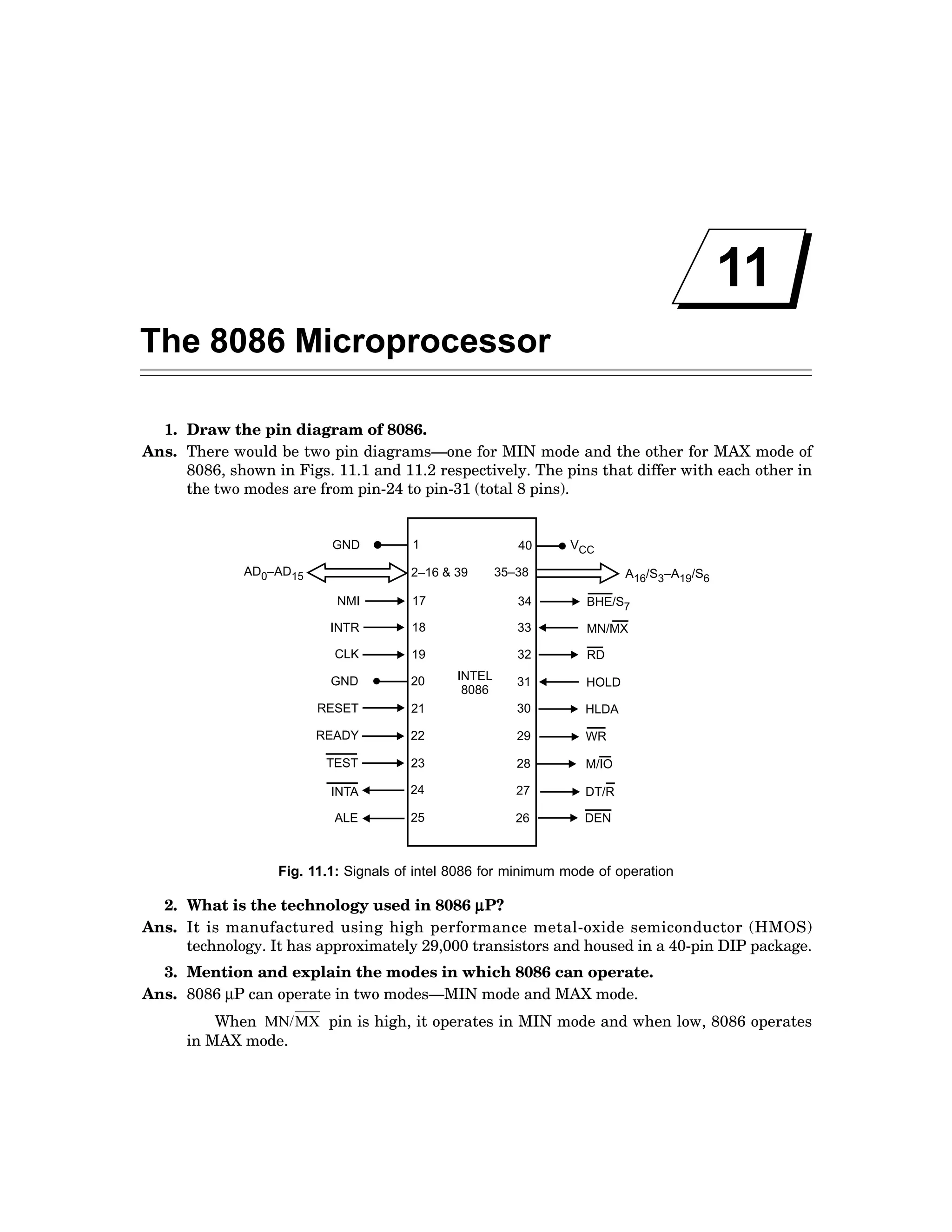
The document discusses the 8086 microprocessor. It provides details about the pin diagram of 8086 in minimum and maximum modes. It mentions that 8086 is manufactured using HMOS technology and has approximately 29,000 transistors housed in a 40-pin DIP package. It can operate in two modes - minimum and maximum mode based on the state of the MN/MX pin. The minimum mode is for a uniprocessor system while maximum mode is for a multiprocessor system.

![The 8086 Microprocessor 201
All the four registers can be used bytewise or wordwise. The alphabets X, H and L
respectively refer to word, higher byte or lower byte respectively of any register.
All the four registers can be used as the source or destination of an operand during
an arithmetic operation such as ADD or logical operation such as AND, although particular
registers are earmarked for specific operations. Register C is used as a count register in
string operations and as such is called a ‘count’ register. Register C is also used for
multibit shift or rotate instructions.
Register D is used to hold the address of I/O port while register A is used for all
I/O operations that require data to be inputted or outputted.
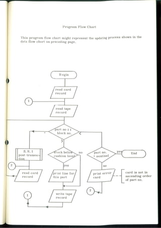
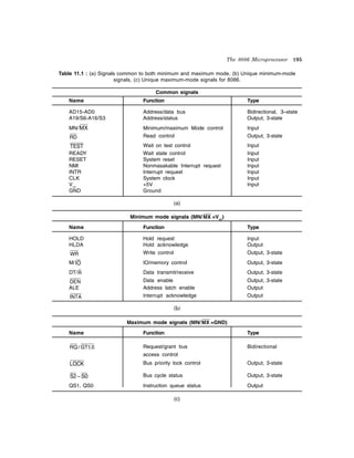
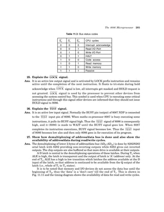
16. Describe the status register of 8086.
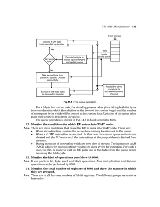
Ans. It is a 16-bit register, also called flag register or Program Status Word (PSW). Seven bits
remain unused while the rest nine are used to indicate the conditions of flags. The status
flags of the register are shown below in Fig. 11.8.
1
2
3
4
5
6
7
8
9
10
11
12
13
14
15 0
x x x x
• OF DF IF TF SF ZF X AF X PF X CF
Overflow flag
Direction flag
Interrupt
enable flag
Trap flag
Bit no.
Status flags
Carry flag
Parity flag
Auxiliary carry flag
Zero flag
Sign flag
Fig.11.8: Status flags of intel 8086
Out of nine flags, six are condition flags and three are control flags. The control flags
are TF (Trap), IF (Interrupt) and DF (Direction) flags, which can be set/reset by the
programmer, while the condition flags [OF (Overflow), SF (Sign), ZF (Zero), AF (Auxiliary
Carry), PF (Parity) and CF (Carry)] are set/reset depending on the results of some
arithmetic or logical operations during program execution.
CF is set if there is a carry out of the MSB position resulting from an addition
operation or if a borrow is needed out of the MSB position during subtraction.
PF is set if the lower 8-bits of the result of an operation contains an even number
of 1’s. AF is set if there is a carry out of bit 3 resulting from an addition operation or a
borrow required from bit 4 into bit 3 during subtraction operation.
ZF is set if the result of an arithmetic or logical operation is zero.
SF is set if the MSB of the result of an operation is 1. SF is used with unsigned
numbers.
OF is used only for signed arithmetic operation and is set if the result is too large
to be fitted in the number of bits available to accommodate it.
The functions of the flags along with their bit positions are shown in Fig. 11.9 below.
Bit position Name Function
0
2
4
CF
PF
AF
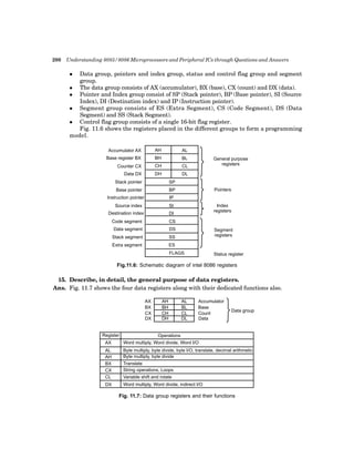
Carry flag: Set on high-order bit carry or borrow; cleared otherwise
Parity flag: Set if low-order 8-bit of result contain an even number
of 1-bit; cleared otherwise
Set on carry from or borrow to the low-order 4-bits of AL; cleared
otherwise](https://image.slidesharecdn.com/computerengineeringiiyear-231127074136-7947370a/85/Computer-Engineering-II-Year-pdf-9-320.jpg)
![202 Understanding 8085/8086 Microprocessors and Peripheral ICs through Questions and Answers
6
7
ZF
SF
Zero flag: Set if result is zero; cleared otherwise
Sign Flag: Set equal to high-order bit of result (0 is positive, 1 if
negative)
8
9
10
TF
IF
DF
Signal step flag: Once set, a single-step interrupt occurs after the
next instruction executes; TF is cleared by the single-step interrupt
Interrupt-enable flag: When set, maskable interrupts will cause
the CPU to transfer control to an interrupt vector specified location.
Direction flag: Causes string instructions to auto decrement the
appropriate index register when set; clearing DF causes auto
11 OF
increment.
Overflow flag: Set if the signed result cannot be expressed within
the number of bits in the destination operand; cleared otherwise.
Fig.11.9: 8086 flags: DF, IF and TF can be set or reset to control
the operations of the processor. The remaining flags are status indicators.
17. Discuss the three control flags of 8086.
Ans. The three control flags of 8086 are TF, IF and DF. These three flags are programmable,
i.e., can be set/reset by the programmer so as to control the operation of the processor.
When TF (trap flag) is set (=1), the processor operates in single stepping mode—i.e.,
pausing after each instruction is executed. This mode is very useful during program
development or program debugging.
When an interrupt is recognised, TF flag is cleared. When the CPU returns to the
main program from ISS (interrupt service subroutine), by execution of IRET in the last
line of ISS, TF flag is restored to its value that it had before interruption.
TF cannot be directly set or reset. So indirectly it is done by pushing the flag register
on the stack, changing TF as desired and then popping the flag register from the stack.
When IF (interrupt flag) is set, the maskable interrupt INTR is enabled otherwise
disabled (i.e., when IF = 0).
IF can be set by executing STI instruction and cleared by CLI instruction. Like TF
flag, when an interrupt is recognised, IF flag is cleared, so that INTR is disabled. In the
last line of ISS when IRET is encountered, IF is restored to its original value.
When 8086 is reset, IF is cleared, i.e., resetted.
DF (direction flag) is used in string (also known as block move) operations. It can be
set by STD instruction and cleared by CLD. If DF is set to 1 and MOVS instruction is
executed, the contents of the index registers DI and SI are automatically decremented
to access the string from the highest memory location down to the lowest memory
location.
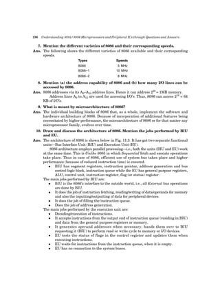
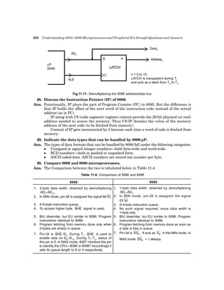
18. Discuss the Pointers and Index group of registers.
Ans. The pointer registers are SP and BP while the index registers are SI and DI.
All the four are 16-bit registers and are used to store offset addresses of memory
locations relative to segment registers. They act as memory pointers. As an example,
MOV AH, [SI] implies, “Move the byte whose address is contained in SI into AH”. If now,
SI = 2000 H, then execution of above instruction will put the value FF H in register
AH, shown in Fig. 11.10, [SI+1 : SI] = ABFF H, where obviously SI+1 points to memory
location 2001 H and [SI+1] = AB H.
SI and DI are also used as general purpose registers. Again in certain string (block
move) instructions, SI and DI are used as source and destination index registers](https://image.slidesharecdn.com/computerengineeringiiyear-231127074136-7947370a/85/Computer-Engineering-II-Year-pdf-10-320.jpg)
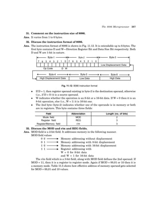
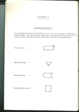
![208 Understanding 8085/8086 Microprocessors and Peripheral ICs through Questions and Answers
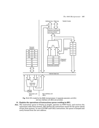
Table 11.5: For effective address calculation, values of MOD and r/m
r/m MOD 00 MOD 01 MOD 10 MOD 11
W = 0 W = 1
000
001
010
011
100
101
110
111
[BX] + [SI]
[BX] + [DI]
[BP] + [SI]
[BP] + [DI]
[SI]
[DI]
Direct Addressing
[BX]
[BX]+[SI]+D8
[BX]+[DI]+D8
[BP]+[SI]+D8
[BP]+[DI]+D8
[SI]+D8
[DI]+D8
[BP]+D8
[BX]+D8
[BX]+[SI]+D16
[BX]+[DI]+D16
[BP]+[SI]+D16
[BP]+[DI]+D16
[SI]+D16
[DI]+D16
[BP]+D16
[BX]+D16
AL
CL
DL
BL
AH
CH
DH
BH
AX
CX
DX
BX
SP
BP
SI
DI
Again, for MOD values 00,01 and 10, the default segment registers selected are shown
in Table 11.6.
Table 11.6: Segment register for various memory addressing modes
r/m MOD 00 MOD 01 MOD 10 Segment Register used
000
001
010
011
100
101
110
111
[BX] + [SI]
[BX] + [DI]
[BP] + [SI]
[BP] + [DI]
[SI]
[DI]
D16 Direct
Addressing
[DS]
[BX]
[BX]+[SI]+DS
[BX]+[DI]+DS
[BP]+[SI]+DS
[BP]+[DI]+DS
[SI]+DS
[DI]+DS
[BP]+DS
Stack pointer
register [SS]
[BX]+DS
[BX]+[SI]+D16
[BX]+[DI]+D16
[BP]+[SI]+D16
[BP]+[DI]+D16
[SI]+D16
[DI]+D16
[BP]+D16
Stack segment
register [SS]
[BX]+D16
DS
DS
SS
SS
DS
DS
DS or SS
as in MOD column
DS
The REG field is a 3-bit field and indicates the register for the first operand which
can be source/destination operand, depending on D = 0/1.
How REG field along with the status of W(0 or 1) select the different registers, is
shown in Table 11.7.
Table 11.7: Definition of registers with ‘W’
REG W = 0 W = 1
000 AL AX
001 CL CX
010 DL DX
011 BL BX
100 AH SP
101 CH BP
110 DH SI
111 BH DI
34. Discuss the instruction format for segment override prefix.
Ans. Default segment selection can be overriden by the override prefix byte, as shown in
below.](https://image.slidesharecdn.com/computerengineeringiiyear-231127074136-7947370a/85/Computer-Engineering-II-Year-pdf-16-320.jpg)
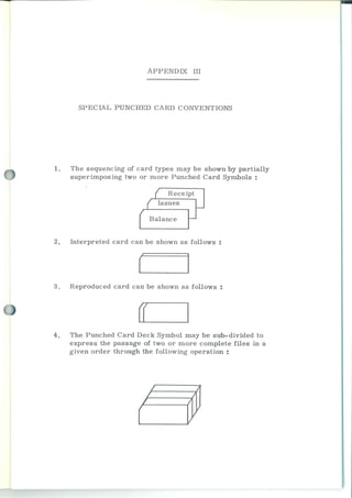
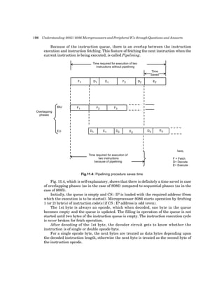
![The 8086 Microprocessor 209
0 0 1 r r 1 1 0
n
Selects Segment
Depending on the 2-bit rr values, the segments selected are shown in Table 11.8.
Table 11.8 : Segment selection by override prefix technique
rr values Segments selected
00 ES
01 CS
10 SS
11 DS
The override prefix byte follows the opcode byte of the instruction, whenever used.
35. Is direct memory to memory data transfer possible in 8086?
Ans. No, 8086 does not have provision for direct memory to memory data transfer.
For this to be implemented, AX is used as an intermediate stage of data. The source
byte (from the memory) is moved into AX register with one instruction. The second
instruction moves the content of AX into destination location (into another memory
location). As example,
MOV AH, [SI]
MOV [DI], AH
Here, the first instruction moves the content of memory location, whose offset
address remains in SI, into AH. The second instruction ensures that the content of AH
is moved into another memory location whose offset address is in DI.
36. Can the data segment (DS) register be loaded directly by its address?
Ans. No, it cannot be done directly. Instead, AX is loaded with the initial address of the DS
register and then it is transferred to DS register, as shown below:
MOV AX, DS ADDR: AX is loaded with initial address of DS register
MOV DS, AX: DS is loaded with AX, i.e., ultimately with DS ADDR
37. Show, in tabular form, the default and alternate segment registers for different
types of memory references.
Ans. Table 11.9 shows the default and alternate register segments which can be used for
different types of memory references.
Table 11.9: Default and alternate register assignments
Type of memory
reference
Default segment Alternative segment Offset (Logical address)
Instruction fetch CS None IP
Stack operation SS None SP, BP
General data DS CS, ES, SS Effective address
String source DS CS, ES, SS SI
String destination ES None DI
BX used as pointer DS CS, ES, SS Effective Address
BP used as pointer SS CS, ES, DS Effective Address](https://image.slidesharecdn.com/computerengineeringiiyear-231127074136-7947370a/85/Computer-Engineering-II-Year-pdf-17-320.jpg)