Download to read offline


This document provides details about an assignment submitted by Mushahadur Rahaman Khan for the course CSE-321. The assignment asks to define the 8086 microprocessor register organization in details. It discusses that the 8086 is a 16-bit microprocessor that can access 1MB of memory. It describes the working of the 8086 including its bus interface unit, execution unit, registers, flags, and provides a block diagram.
Introduction to the assignment topic on 8086 Microprocessor, course details, submission information.
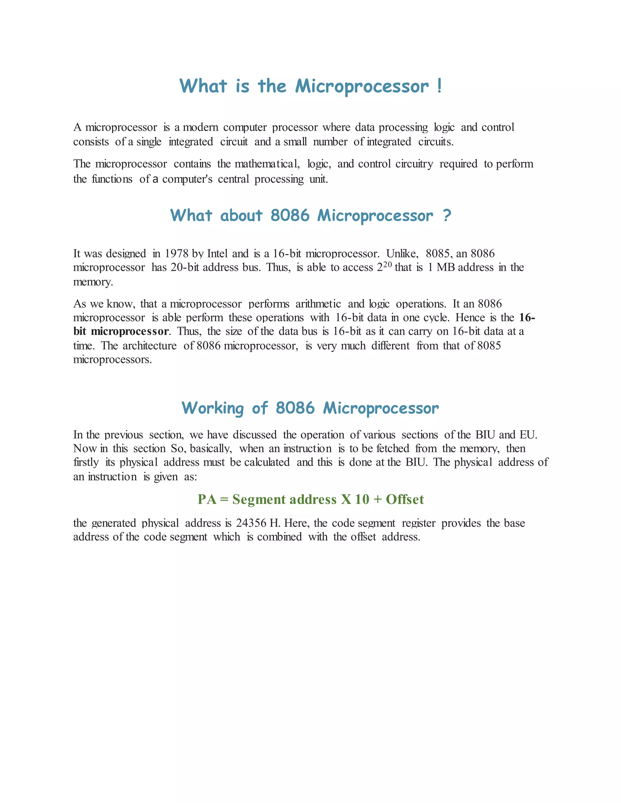
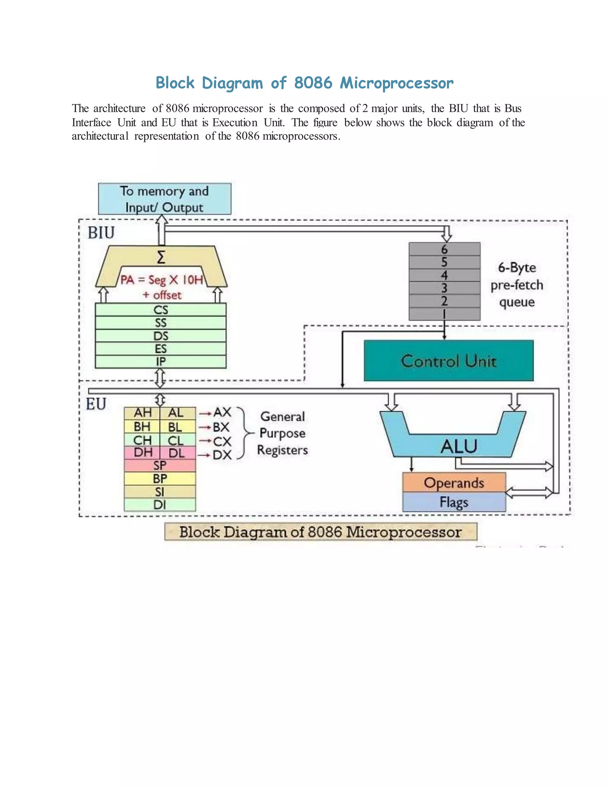
Definition and overview of microprocessors; focus on 8086, its 16-bit architecture, and 1 MB address capacity.Details on the operation of 8086, including address calculation, instruction fetching, and control unit functions.
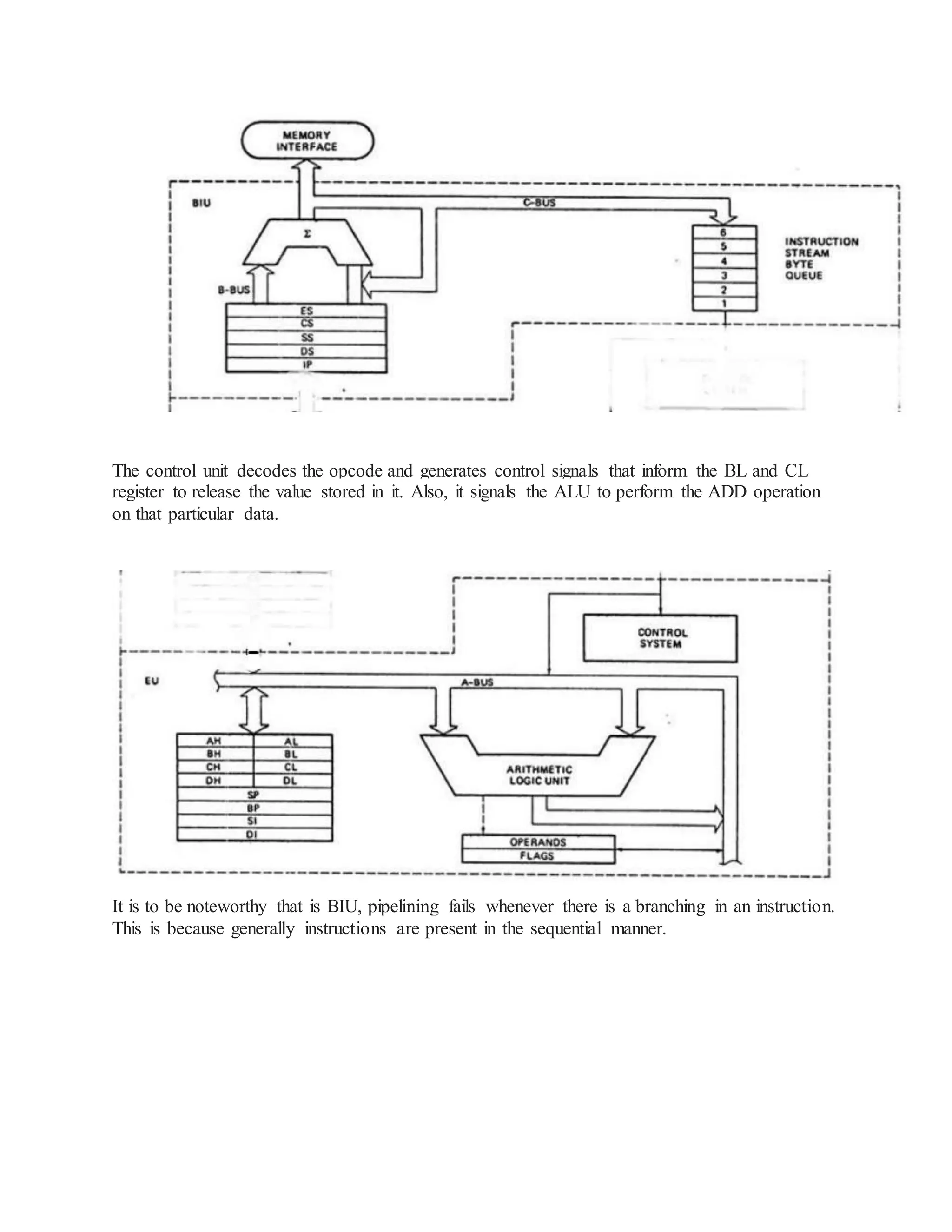
Block diagram of 8086 architecture showing the Bus Interface Unit (BIU) and Execution Unit (EU).
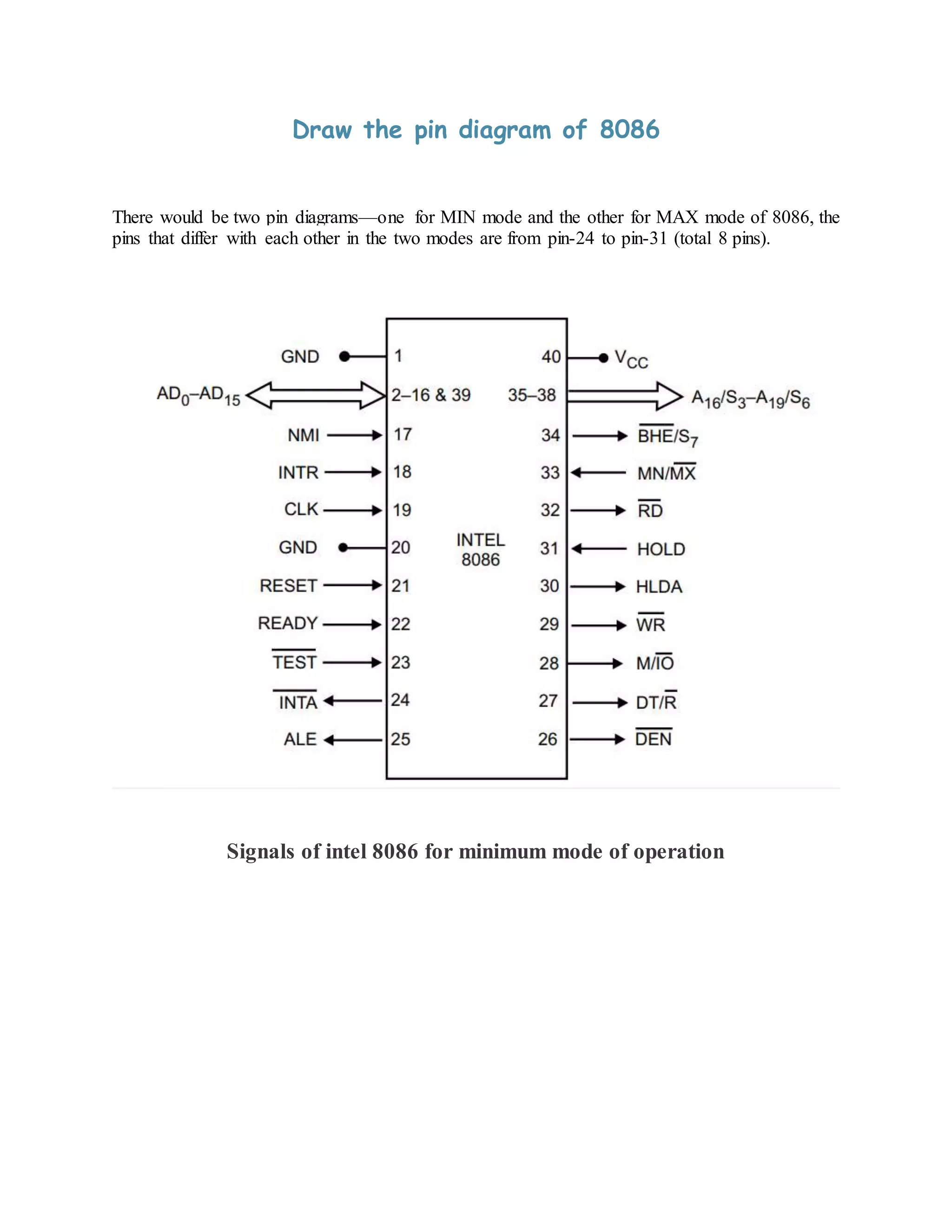
Description of pin diagrams for MIN and MAX modes, detailing the key pin differences.
Role of BIU in instruction fetching, memory addressing, and the instruction queue in 8086.
Description of the EU's control unit, ALU, and general-purpose registers functionality.
Overview of pointer, index, and control flags registers, their functions in the EU.