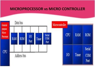
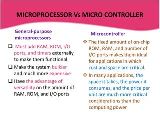
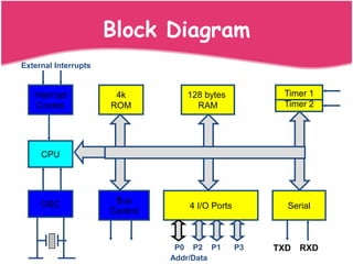
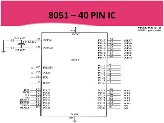
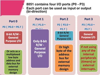
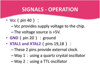
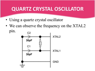
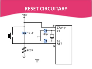
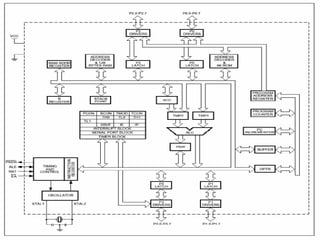
MICROCONTROLLERS
           8051
WHAT IS A MICROCONTROLLER?
• All of the components needed for a controller
  were built right onto one chip.
• A one chip computer, or microcontroller was
  born.
• A microcontroller is a highly integrated chip
  which includes, on one chip, all or most of the
  parts needed for a controller.
• The microcontroller could be called a "one-
  chip solution".
MICROPROCESSOR vs MICRO CONTROLLER
MICROPROCESSOR Vs MICRO CONTROLLER

   General-purpose                  Microcontroller
   microprocessors
                                  The fixed amount of on-chip
 Must add RAM, ROM, I/O           ROM, RAM, and number of
  ports, and timers externally     I/O ports makes them ideal
  to make them functional          for applications in which
 Make the system bulkier          cost and space are critical.
  and much more expensive         In many applications, the
 Have the advantage of            space it takes, the power it
  versatility on the amount of     consumes, and the price per
  RAM, ROM, and I/O ports          unit are much more critical
                                   considerations than the
                                   computing power
Features :
• The Intel 8051 is used in embedded
  systems
  – 8-bit CPU
  – 4k bytes ROM for the program
  – 128 BYTES of RAM for variables
  – 32 I/O lines ( 4 PORTS WITH 8 EACH )
  – 2 timers
  – 1 Serial port
  – 6 interrupt sources
  – Low cost (10-15 cents per chip)
Block Diagram
External Interrupts


   Interrupt           4k          128 bytes           Timer 1
    Control           ROM            RAM               Timer 2


     CPU


     OSC               Bus
                                   4 I/O Ports          Serial
                      Control


                                 P0 P2 P1        P3   TXD   RXD
                                Addr/Data
8051 – PIN DIAGRAM
8051 – 40 PIN IC
• 8051 contains four I/O ports (P0 - P3)
                 • Each port can be used as input or output
                   (bi-direction)

                        Port 1          Port 2        Port 3
    Port 0
                       P1(P1.0~       P2(P2.0~       P3(P3.0~
P0(P0.0~P0.7)
                        P1.7)           P2.7)         P3.7)
                                      8-bit R/W -
 8-bit R/W -                                          General
                                        General
   General                                          Purpose I/O
                                      Purpose I/O
 Purpose I/O           Only 8-bit
                         R/W -
                        General       Or high       if not using
  Or acts as a          Purpose      byte of the     any of the
  multiplexed
                          I/O         address          internal
   low byte                            bus for      peripherals
  address and                                       (timers) or
  data bus for
                                      external
    external                          memory          external
   memory                              design       interrupts.
     design
PORT 3 – MULTIPLE FUNCTIONS
IMPORTANT PINS

•   PSEN (out): Program Store Enable, the read signal
    for external program memory (active low).
•   ALE (out): Address Latch Enable, to latch address
    outputs at Port0 and Port2
•   EA (in): External Access Enable, active low to access
    external program memory locations 0 to 4K
•   RXD,TXD: UART pins for serial I/O on Port 3
•   XTAL1 & XTAL2: Crystal inputs for internal
    oscillator.
SIGNALS - OPERATION
• Vcc(pin 40):
   – Vcc provides supply voltage to the chip.
   – The voltage source is +5V.
• GND(pin 20):ground
• XTAL1 and XTAL2(pins 19,18):
   – These 2 pins provide external clock.
   – Way 1:using a quartz crystal oscillator
   – Way 2:using a TTL oscillator
QUARTZ CRYSTAL OSCILLATOR
• Using a quartz crystal oscillator
• We can observe the frequency on the XTAL2
  pin.      C2
                         XTAL2
          30pF

           C1
                         XTAL1
          30pF

                         GND
XTAL Connection to an External Clock Source


• Using a TTL oscillator
• XTAL2 is unconnected.
             N             XTAL2
             C

           EXTERNAL
           OSCILLATOR
           SIGNAL          XTAL1


                           GND
RST - RESET
• RST(pin 9):reset
   – input pin and active high
       • The high pulse must be high at least 2 machine
         cycles.
   – power-on reset.
       • Upon applying a high pulse to RST, the
         microcontroller will reset and all values in
         registers will be lost.
       • Reset values of some 8051 registers
RESET Value of Some 8051 Registers:


 Register           Reset Value

 PC                 0000

 ACC                0000

 B                  0000

 PSW                0000

 SP                 0007

 DPTR               0000

 RAM are all zero
RESET CIRCUITARY
Vcc


                      31
                           EA/VPP
                           X1
      10 uF   30 pF

                           X2
                           RST
                      9
      8.2 K
EA’ & PSEN’
• EA’(pin 31):external access
   – There is no on-chip ROM in 8031 and 8032 .
   – The EA’ pin is connected to GND to indicate
     the code is stored externally.
   – PSEN’ & ALE are used for external ROM.
   – For 8051, EA’ pin is connected to Vcc.
   – active low.
• PSEN’(pin 29):program store enable
   – This is an output pin and is connected to the OE
     pin of the ROM.
ALE
ALE(pin 30):address
latch enable
   It is an output pin and is
   active high.
   8051 port 0 provides
   both address and data.
   The ALE pin is used for
   de-multiplexing the
   address and data by
   connecting to the G pin of
   the 74LS373 latch.
External code memory

       WR
       RD
     PSEN                      OE
      ALE            74LS373   CS
             G
     P0.0                      A0
                 D
     P0.7                      A7


                               D0
                               D7
EA
     P2.0                      A8
      P2.7                     A15

 8051                          ROM
External data memory
       WR                      WR
       RD                      RD
     PSEN
      ALE            74LS373   CS
             G
     P0.0                      A0
                 D
     P0.7                      A7


                               D0
                               D7
EA
     P2.0                      A8
      P2.7                     A15

 8051                          RAM
Title

• Lorem ipsum dolor sit amet, consectetuer
  adipiscing elit. Vivamus et magna. Fusce sed
  sem sed magna suscipit egestas.
• Lorem ipsum dolor sit amet, consectetuer
  adipiscing elit. Vivamus et magna. Fusce sed
  sem sed magna suscipit egestas.

8051 microprocessor

  • 1.
  • 2.
    WHAT IS AMICROCONTROLLER? • All of the components needed for a controller were built right onto one chip. • A one chip computer, or microcontroller was born. • A microcontroller is a highly integrated chip which includes, on one chip, all or most of the parts needed for a controller. • The microcontroller could be called a "one- chip solution".
  • 3.
  • 4.
    MICROPROCESSOR Vs MICROCONTROLLER General-purpose Microcontroller microprocessors  The fixed amount of on-chip  Must add RAM, ROM, I/O ROM, RAM, and number of ports, and timers externally I/O ports makes them ideal to make them functional for applications in which  Make the system bulkier cost and space are critical. and much more expensive  In many applications, the  Have the advantage of space it takes, the power it versatility on the amount of consumes, and the price per RAM, ROM, and I/O ports unit are much more critical considerations than the computing power
  • 5.
    Features : • TheIntel 8051 is used in embedded systems – 8-bit CPU – 4k bytes ROM for the program – 128 BYTES of RAM for variables – 32 I/O lines ( 4 PORTS WITH 8 EACH ) – 2 timers – 1 Serial port – 6 interrupt sources – Low cost (10-15 cents per chip)
  • 6.
    Block Diagram External Interrupts Interrupt 4k 128 bytes Timer 1 Control ROM RAM Timer 2 CPU OSC Bus 4 I/O Ports Serial Control P0 P2 P1 P3 TXD RXD Addr/Data
  • 7.
    8051 – PINDIAGRAM
  • 8.
  • 9.
    • 8051 containsfour I/O ports (P0 - P3) • Each port can be used as input or output (bi-direction) Port 1 Port 2 Port 3 Port 0 P1(P1.0~ P2(P2.0~ P3(P3.0~ P0(P0.0~P0.7) P1.7) P2.7) P3.7) 8-bit R/W - 8-bit R/W - General General General Purpose I/O Purpose I/O Purpose I/O Only 8-bit R/W - General Or high if not using Or acts as a Purpose byte of the any of the multiplexed I/O address internal low byte bus for peripherals address and (timers) or data bus for external external memory external memory design interrupts. design
  • 10.
    PORT 3 –MULTIPLE FUNCTIONS
  • 11.
    IMPORTANT PINS • PSEN (out): Program Store Enable, the read signal for external program memory (active low). • ALE (out): Address Latch Enable, to latch address outputs at Port0 and Port2 • EA (in): External Access Enable, active low to access external program memory locations 0 to 4K • RXD,TXD: UART pins for serial I/O on Port 3 • XTAL1 & XTAL2: Crystal inputs for internal oscillator.
  • 12.
    SIGNALS - OPERATION •Vcc(pin 40): – Vcc provides supply voltage to the chip. – The voltage source is +5V. • GND(pin 20):ground • XTAL1 and XTAL2(pins 19,18): – These 2 pins provide external clock. – Way 1:using a quartz crystal oscillator – Way 2:using a TTL oscillator
  • 13.
    QUARTZ CRYSTAL OSCILLATOR •Using a quartz crystal oscillator • We can observe the frequency on the XTAL2 pin. C2 XTAL2 30pF C1 XTAL1 30pF GND
  • 14.
    XTAL Connection toan External Clock Source • Using a TTL oscillator • XTAL2 is unconnected. N XTAL2 C EXTERNAL OSCILLATOR SIGNAL XTAL1 GND
  • 15.
    RST - RESET •RST(pin 9):reset – input pin and active high • The high pulse must be high at least 2 machine cycles. – power-on reset. • Upon applying a high pulse to RST, the microcontroller will reset and all values in registers will be lost. • Reset values of some 8051 registers
  • 16.
    RESET Value ofSome 8051 Registers: Register Reset Value PC 0000 ACC 0000 B 0000 PSW 0000 SP 0007 DPTR 0000 RAM are all zero
  • 17.
    RESET CIRCUITARY Vcc 31 EA/VPP X1 10 uF 30 pF X2 RST 9 8.2 K
  • 18.
    EA’ & PSEN’ •EA’(pin 31):external access – There is no on-chip ROM in 8031 and 8032 . – The EA’ pin is connected to GND to indicate the code is stored externally. – PSEN’ & ALE are used for external ROM. – For 8051, EA’ pin is connected to Vcc. – active low. • PSEN’(pin 29):program store enable – This is an output pin and is connected to the OE pin of the ROM.
  • 19.
    ALE ALE(pin 30):address latch enable It is an output pin and is active high. 8051 port 0 provides both address and data. The ALE pin is used for de-multiplexing the address and data by connecting to the G pin of the 74LS373 latch.
  • 20.
    External code memory WR RD PSEN OE ALE 74LS373 CS G P0.0 A0 D P0.7 A7 D0 D7 EA P2.0 A8 P2.7 A15 8051 ROM
  • 21.
    External data memory WR WR RD RD PSEN ALE 74LS373 CS G P0.0 A0 D P0.7 A7 D0 D7 EA P2.0 A8 P2.7 A15 8051 RAM
  • 23.
    Title • Lorem ipsumdolor sit amet, consectetuer adipiscing elit. Vivamus et magna. Fusce sed sem sed magna suscipit egestas. • Lorem ipsum dolor sit amet, consectetuer adipiscing elit. Vivamus et magna. Fusce sed sem sed magna suscipit egestas.