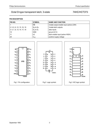
SlideShare a Scribd company logo
INTEGRATED CIRCUITS


  DATA SHEET
     For a complete data sheet, please also download:

     • The IC06 74HC/HCT/HCU/HCMOS Logic Family Specifications
     • The IC06 74HC/HCT/HCU/HCMOS Logic Package Information
     • The IC06 74HC/HCT/HCU/HCMOS Logic Package Outlines


  74HC/HCT373
  Octal D-type transparent latch;
  3-state
Product specification                                September 1993
File under Integrated Circuits, IC06
Philips Semiconductors                                                                                  Product specification


  Octal D-type transparent latch; 3-state                                                           74HC/HCT373

FEATURES                                                          input and an output enable (OE) input are common to all
                                                                  latches.
• 3-state non-inverting outputs for bus oriented
  applications                                                    The “373” consists of eight D-type transparent latches with
• Common 3-state output enable input                              3-state true outputs. When LE is HIGH, data at the Dn
                                                                  inputs enters the latches. In this condition the latches are
• Functionally identical to the “563”, “573” and “533”            transparent, i.e. a latch output will change state each time
• Output capability: bus driver                                   its corresponding D-input changes.
• ICC category: MSI                                               When LE is LOW the latches store the information that was
                                                                  present at the D-inputs a set-up time preceding the
GENERAL DESCRIPTION                                               HIGH-to-LOW transition of LE. When OE is LOW, the
                                                                  contents of the 8 latches are available at the outputs.
The 74HC/HCT373 are high-speed Si-gate CMOS devices               When OE is HIGH, the outputs go to the high impedance
and are pin compatible with low power Schottky TTL                OFF-state. Operation of the OE input does not affect the
(LSTTL). They are specified in compliance with JEDEC              state of the latches.
standard no. 7A.
                                                                  The “373” is functionally identical to the “533”, “563” and
The 74HC/HCT373 are octal D-type transparent latches              “573”, but the “563” and “533” have inverted outputs and
featuring separate D-type inputs for each latch and 3-state       the “563” and “573” have a different pin arrangement.
outputs for bus oriented applications. A latch enable (LE)

QUICK REFERENCE DATA
GND = 0 V; Tamb = 25 °C; tr = tf = 6 ns

                                                                                                    TYPICAL
     SYMBOL                       PARAMETER                                CONDITIONS                                  UNIT
                                                                                                    HC      HCT
tPHL/ tPLH        propagation delay                                 CL = 15 pF; VCC = 5 V
                    Dn to Qn                                                                      12       14     ns
                    LE to Qn                                                                      15       13     ns
CI                input capacitance                                                               3.5      3.5    pF
CPD               power dissipation capacitance per latch           notes 1 and 2                 45       41     pF

Notes
1. CPD is used to determine the dynamic power dissipation (PD in µW):
       PD = CPD × VCC2 × fi + ∑ (CL × VCC2 × fo) where:
   fi = input frequency in MHz
   fo = output frequency in MHz
   ∑ (CL × VCC2 × fo) = sum of outputs
   CL = output load capacitance in pF
   VCC = supply voltage in V
2. For HC the condition is VI = GND to VCC. For HCT the condition is VI = GND to VCC − 1.5 V


ORDERING INFORMATION
See “74HC/HCT/HCU/HCMOS Logic Package Information”.


September 1993                                                2
Philips Semiconductors                                                                    Product specification


    Octal D-type transparent latch; 3-state                                            74HC/HCT373

PIN DESCRIPTION

PIN NO.                          SYMBOL             NAME AND FUNCTION
1                                OE                 3-state output enable input (active LOW)
2, 5, 6, 9, 12, 15, 16, 19       Q0 to Q7           3-state latch outputs
3, 4, 7, 8, 13, 14, 17, 18       D0 to D7           data inputs
10                               GND                ground (0 V)
11                               LE                 latch enable input (active HIGH)
20                               VCC                positive supply voltage


      Fig.1 Pin configuration.              Fig.2 Logic symbol.                  Fig.3 IEC logic symbol.


September 1993                                      3
Philips Semiconductors                                                                         Product specification


  Octal D-type transparent latch; 3-state                                                  74HC/HCT373

                                                           FUNCTION TABLE

                                                           OPERATING   INPUTS             INTERNAL      OUTPUTS
                                                             MODES   OE LE Dn              LATCHES       Q0 to Q7
                                                           enable and       L   H     L        L             L
                                                           read
                                                           register         L   H     H        H             H
                                                           (transparent
                                                           mode)
                                                           latch and        L    L    l        L             L
                                                           read register    L    L    h        H             H
                                                           latch register   H    X    X        X             Z
                                                           and disable      H    X    X        X             Z
                                                           outputs
                                                           Notes
              Fig.4 Functional diagram.
                                                           1. H = HIGH voltage level
                                                              h = HIGH voltage level one set-up time prior to the
                                                                     HIGH-to-LOW LE transition
                                                              L = LOW voltage level
                                                              I = LOW voltage level one set-up time prior to the
                                                                     HIGH-to-LOW LE transition
                                                              X = don’t care
                                                              Z = high impedance OFF-state


           Fig.5 Logic diagram (one latch).


                                              Fig.6 Logic diagram.


September 1993                                         4
Philips Semiconductors                                                                             Product specification


     Octal D-type transparent latch; 3-state                                                      74HC/HCT373

DC CHARACTERISTICS FOR 74HC
For the DC characteristics see “74HC/HCT/HCU/HCMOS Logic Family Specifications”.
Output capability: bus driver
ICC category: MSI


AC CHARACTERISTICS FOR 74HC
GND = 0 V; tr = tf = 6 ns; CL = 50 pF

                                                                Tamb (°C)                          TEST CONDITIONS
                                                                 74HC
 SYMBOL            PARAMETER                                                                 UNIT V    WAVEFORMS
                                                +25               −40 to +85   −40 to +125          CC
                                                                                                  (V)
                                           min. typ. max. min. max. min.             max.
tPHL/ tPLH   propagation delay                  41    150               190          225     ns    2.0   Fig.7
              Dn to Qn                          15    30                38           45            4.5
                                                12    26                33           38            6.0
tPHL/ tPLH   propagation delay                  50    175               220          265     ns    2.0   Fig.8
              LE to Qn                          18    35                44           53            4.5
                                                14    30                37           45            6.0
tPZH/ tPZL   3-state output enable time         44    150               190          225     ns    2.0   Fig.9
              OE to Qn                          16    30                38           45            4.5
                                                13    26                33           38            6.0
tPHZ/ tPLZ   3-state output disable time        47    150               190          225     ns    2.0   Fig.9
              OE to Qn                          17    30                38           45            4.5
                                                14    26                33           38            6.0
tTHL/ tTLH   output transition time             14    60                75           90      ns    2.0   Fig.7
                                                5     12                15           18            4.5
                                                4     10                13           15            6.0
tW           LE pulse width                80   17               100           120           ns    2.0   Fig.8
              HIGH                         16   6                20            24                  4.5
                                           14   5                17            20                  6.0
tsu          set-up time                   50   14               65            75            ns    2.0   Fig.10
              Dn to LE                     10   5                13            15                  4.5
                                           9    4                11            13                  6.0
th           hold time                     5    −8               5             5             ns    2.0   Fig.10
              Dn to LE                     5    −3               5             5                   4.5
                                           5    −2               5             5                   6.0


September 1993                                              5
Philips Semiconductors                                                                                 Product specification


     Octal D-type transparent latch; 3-state                                                        74HC/HCT373

DC CHARACTERISTICS FOR 74HCT
For the DC characteristics see “74HC/HCT/HCU/HCMOS Logic Family Specifications”.
Output capability: bus driver
ICC category: MSI

Note to HCT types
The value of additional quiescent supply current (∆ICC) for a unit load of 1 is given in the family specifications.
To determine ∆ICC per input, multiply this value by the unit load coefficient shown in the table below.


INPUT          UNIT LOAD COEFFICIENT
Dn             0.30
LE             1.50
OE             1.00


AC CHARACTERISTICS FOR 74HCT
GND = 0 V; tr = tf = 6 ns; CL = 50 pF

                                                                  Tamb (°C)                           TEST CONDITIONS
                                                                   74HCT
 SYMBOL               PARAMETER                                                                UNIT V    WAVEFORMS
                                                   +25              −40 to +85   −40 to +125          CC
                                                                                                    (V)
                                           min. typ. max. min. max. min.               max.
tPHL/ tPLH   propagation delay                    17     30              38           45       ns     4.5   Fig.7
              Dn to Qn
tPHL/ tPLH   propagation delay                    16     32              40           48       ns     4.5   Fig.8
              LE to Qn
tPZH/ tPZL   3-state output enable time           19     32              40           48       ns     4.5   Fig.9
              OE to Qn
tPHZ/ tPLZ   3-state output disable time          18     30              38           45       ns     4.5   Fig.9
              OE to Qn
tTHL/ tTLH   output transition time               5      12              15           18       ns     4.5   Fig.7

tW           LE pulse width                16     4                20            24            ns     4.5   Fig.8
              HIGH
tsu          set-up time                   12     6                15            18            ns     4.5   Fig.10
              Dn to LE
th           hold time                     4      −1               4             4             ns     4.5   Fig.10
              Dn to LE


September 1993                                                6
Philips Semiconductors                                                                                        Product specification


  Octal D-type transparent latch; 3-state                                                                 74HC/HCT373

AC WAVEFORMS


                                                                     (1) HC : VM = 50%; VI = GND to VCC.
                                                                         HCT : VM = 1.3 V; VI = GND to 3 V.
   (1) HC : VM = 50%; VI = GND to VCC.
       HCT : VM = 1.3 V; VI = GND to 3 V.
                                                                     Fig.8    Waveforms showing the latch enable input
   Fig.7     Waveforms showing the input (Dn) to output                       (LE) pulse width, the latch enable input to
             (Qn) propagation delays and the output                           output (Qn) propagation delays and the
             transition times.                                                output transition times.


   (1) HC : VM = 50%; VI = GND to VCC.
       HCT : VM = 1.3 V; VI = GND to 3 V.


                                  Fig.9 Waveforms showing the 3-state enable and disable times.


   The shaded areas indicate when the input is permitted to
   change for predictable output performance.
   (1) HC : VM = 50%; VI = GND to VCC.
       HCT : VM = 1.3 V; VI = GND to 3 V.


                      Fig.10 Waveforms showing the data set-up and hold times for Dn input to LE input.


September 1993                                                 7
Philips Semiconductors                                  Product specification


  Octal D-type transparent latch; 3-state              74HC/HCT373

PACKAGE OUTLINES
See “74HC/HCT/HCU/HCMOS Logic Package Outlines”.


September 1993                                     8
This datasheet has been download from:

      www.datasheetcatalog.com

Datasheets for electronics components.

More Related Content

What's hot

Digital Logic circuit
Digital Logic circuitDigital Logic circuit
Digital Logic circuit
kavitha muneeshwaran
 
Combinational circuits
Combinational circuitsCombinational circuits
Combinational circuits
Jamnas Mundakkutty A
 
Switches and LEDs interface to the 8051 microcontroller
Switches and LEDs interface to the 8051 microcontrollerSwitches and LEDs interface to the 8051 microcontroller
Switches and LEDs interface to the 8051 microcontroller
University of Technology - Iraq
 
Analysis and design of analog integrated circuits
Analysis and design of analog integrated circuitsAnalysis and design of analog integrated circuits
Analysis and design of analog integrated circuits
Badam Gantumur
 
Finite State Machine.ppt.pptx
Finite State Machine.ppt.pptxFinite State Machine.ppt.pptx
Finite State Machine.ppt.pptx
SKUP1
 
Introduction to embedded system design
Introduction to embedded system designIntroduction to embedded system design
Introduction to embedded system design
Mukesh Bansal
 
Embedded systems, 8051 microcontroller
Embedded systems, 8051 microcontrollerEmbedded systems, 8051 microcontroller
Embedded systems, 8051 microcontroller
Amandeep Alag
 
Clocked Sequential circuit analysis and design
Clocked Sequential circuit analysis and designClocked Sequential circuit analysis and design
Clocked Sequential circuit analysis and design
Dr Naim R Kidwai
 
Modeling Style and Delay Model of VHDL By Ap
Modeling Style and Delay Model of VHDL By ApModeling Style and Delay Model of VHDL By Ap
Modeling Style and Delay Model of VHDL By Ap
Er. Ashish Pandey
 
Cyclone II FPGA Overview
Cyclone II FPGA OverviewCyclone II FPGA Overview
Cyclone II FPGA Overview
Premier Farnell
 
Mp &mc programs
Mp &mc programsMp &mc programs
Mp &mc programs
Haritha Hary
 
Sequential circuit design
Sequential circuit designSequential circuit design
Sequential circuit design
Satya P. Joshi
 
Interrupt in real time system
Interrupt in real time system Interrupt in real time system
Interrupt in real time system
ali jawad
 
FPGA Tutorial - LCD Interface
FPGA Tutorial - LCD InterfaceFPGA Tutorial - LCD Interface
FPGA Tutorial - LCD Interface
Politeknik Elektronika Negeri Surabaya
 
Decoders-Digital Electronics
Decoders-Digital ElectronicsDecoders-Digital Electronics
Decoders-Digital Electronics
Paurav Shah
 
Registers and counters
Registers and countersRegisters and counters
Registers and counters
Heman Pathak
 
L12 programmable+logic+devices+(pld)
L12 programmable+logic+devices+(pld)L12 programmable+logic+devices+(pld)
L12 programmable+logic+devices+(pld)
NAGASAI547
 
chap 18 multicore computers
chap 18 multicore computers chap 18 multicore computers
chap 18 multicore computers
Sher Shah Merkhel
 
Combinational & Sequential ATPG.pdf
Combinational & Sequential ATPG.pdfCombinational & Sequential ATPG.pdf
Combinational & Sequential ATPG.pdf
MoinPasha12
 
bus and memory tranfer (computer organaization)
bus and memory tranfer (computer organaization)bus and memory tranfer (computer organaization)
bus and memory tranfer (computer organaization)
Siddhi Viradiya
 

What's hot (20)

Digital Logic circuit
Digital Logic circuitDigital Logic circuit
Digital Logic circuit
 
Combinational circuits
Combinational circuitsCombinational circuits
Combinational circuits
 
Switches and LEDs interface to the 8051 microcontroller
Switches and LEDs interface to the 8051 microcontrollerSwitches and LEDs interface to the 8051 microcontroller
Switches and LEDs interface to the 8051 microcontroller
 
Analysis and design of analog integrated circuits
Analysis and design of analog integrated circuitsAnalysis and design of analog integrated circuits
Analysis and design of analog integrated circuits
 
Finite State Machine.ppt.pptx
Finite State Machine.ppt.pptxFinite State Machine.ppt.pptx
Finite State Machine.ppt.pptx
 
Introduction to embedded system design
Introduction to embedded system designIntroduction to embedded system design
Introduction to embedded system design
 
Embedded systems, 8051 microcontroller
Embedded systems, 8051 microcontrollerEmbedded systems, 8051 microcontroller
Embedded systems, 8051 microcontroller
 
Clocked Sequential circuit analysis and design
Clocked Sequential circuit analysis and designClocked Sequential circuit analysis and design
Clocked Sequential circuit analysis and design
 
Modeling Style and Delay Model of VHDL By Ap
Modeling Style and Delay Model of VHDL By ApModeling Style and Delay Model of VHDL By Ap
Modeling Style and Delay Model of VHDL By Ap
 
Cyclone II FPGA Overview
Cyclone II FPGA OverviewCyclone II FPGA Overview
Cyclone II FPGA Overview
 
Mp &mc programs
Mp &mc programsMp &mc programs
Mp &mc programs
 
Sequential circuit design
Sequential circuit designSequential circuit design
Sequential circuit design
 
Interrupt in real time system
Interrupt in real time system Interrupt in real time system
Interrupt in real time system
 
FPGA Tutorial - LCD Interface
FPGA Tutorial - LCD InterfaceFPGA Tutorial - LCD Interface
FPGA Tutorial - LCD Interface
 
Decoders-Digital Electronics
Decoders-Digital ElectronicsDecoders-Digital Electronics
Decoders-Digital Electronics
 
Registers and counters
Registers and countersRegisters and counters
Registers and counters
 
L12 programmable+logic+devices+(pld)
L12 programmable+logic+devices+(pld)L12 programmable+logic+devices+(pld)
L12 programmable+logic+devices+(pld)
 
chap 18 multicore computers
chap 18 multicore computers chap 18 multicore computers
chap 18 multicore computers
 
Combinational & Sequential ATPG.pdf
Combinational & Sequential ATPG.pdfCombinational & Sequential ATPG.pdf
Combinational & Sequential ATPG.pdf
 
bus and memory tranfer (computer organaization)
bus and memory tranfer (computer organaization)bus and memory tranfer (computer organaization)
bus and memory tranfer (computer organaization)
 

Viewers also liked

74hc4020
74hc402074hc4020
74hc4020
nishdevan
 
FFEA 2016 -10 Website Mistakes Even Great Marketers Can Make
FFEA 2016 -10 Website Mistakes Even Great Marketers Can MakeFFEA 2016 -10 Website Mistakes Even Great Marketers Can Make
FFEA 2016 -10 Website Mistakes Even Great Marketers Can Make
Saffire
 
5 Steps To A Smart Compensation Plan
5 Steps To A Smart Compensation Plan5 Steps To A Smart Compensation Plan
5 Steps To A Smart Compensation Plan
BambooHR
 
Stay Up To Date on the Latest Happenings in the Boardroom: Recommended Summer...
Stay Up To Date on the Latest Happenings in the Boardroom: Recommended Summer...Stay Up To Date on the Latest Happenings in the Boardroom: Recommended Summer...
Stay Up To Date on the Latest Happenings in the Boardroom: Recommended Summer...
Stanford GSB Corporate Governance Research Initiative
 
10 Tips for WeChat
10 Tips for WeChat10 Tips for WeChat
10 Tips for WeChat
Chris Baker
 
Benefits of drinking water
Benefits of drinking waterBenefits of drinking water
Benefits of drinking water
Eason Chan
 
20 Ideas for your Website Homepage Content
20 Ideas for your Website Homepage Content20 Ideas for your Website Homepage Content
20 Ideas for your Website Homepage Content
Barry Feldman
 

Viewers also liked (7)

74hc4020
74hc402074hc4020
74hc4020
 
FFEA 2016 -10 Website Mistakes Even Great Marketers Can Make
FFEA 2016 -10 Website Mistakes Even Great Marketers Can MakeFFEA 2016 -10 Website Mistakes Even Great Marketers Can Make
FFEA 2016 -10 Website Mistakes Even Great Marketers Can Make
 
5 Steps To A Smart Compensation Plan
5 Steps To A Smart Compensation Plan5 Steps To A Smart Compensation Plan
5 Steps To A Smart Compensation Plan
 
Stay Up To Date on the Latest Happenings in the Boardroom: Recommended Summer...
Stay Up To Date on the Latest Happenings in the Boardroom: Recommended Summer...Stay Up To Date on the Latest Happenings in the Boardroom: Recommended Summer...
Stay Up To Date on the Latest Happenings in the Boardroom: Recommended Summer...
 
10 Tips for WeChat
10 Tips for WeChat10 Tips for WeChat
10 Tips for WeChat
 
Benefits of drinking water
Benefits of drinking waterBenefits of drinking water
Benefits of drinking water
 
20 Ideas for your Website Homepage Content
20 Ideas for your Website Homepage Content20 Ideas for your Website Homepage Content
20 Ideas for your Website Homepage Content
 

Similar to 74hc373 data sheet

abc song
abc songabc song
abc song
triquyennhi1
 
74 hc hct14_cnv_2
74 hc hct14_cnv_274 hc hct14_cnv_2
74 hc hct14_cnv_2
Adolfo Palomino Naranjo
 
Logic Gates & Family.pdf
Logic Gates & Family.pdfLogic Gates & Family.pdf
Logic Gates & Family.pdf
DanishKhan313548
 
74154datasheet.pdf
74154datasheet.pdf74154datasheet.pdf
74154datasheet.pdf
EFran9
 
74ls373
74ls37374ls373
74ls373
holinh7
 
Promo book2 ch1_feb23_11
Promo book2 ch1_feb23_11Promo book2 ch1_feb23_11
Promo book2 ch1_feb23_11
Sarah Krystelle
 
Badal sharma
Badal sharmaBadal sharma
Badal sharma
badaldausa
 
Interfacing of 8255 IC By Er. Swapnil Kaware.
Interfacing of 8255 IC By Er. Swapnil Kaware.Interfacing of 8255 IC By Er. Swapnil Kaware.
Interfacing of 8255 IC By Er. Swapnil Kaware.
Prof. Swapnil V. Kaware
 
Ig2616051609
Ig2616051609Ig2616051609
Ig2616051609
IJERA Editor
 
combinational logic circuit and sequential logic circuit.pptx
combinational logic circuit and sequential logic circuit.pptxcombinational logic circuit and sequential logic circuit.pptx
combinational logic circuit and sequential logic circuit.pptx
AhmedLakhwera
 
DataSheet 74ls90
DataSheet 74ls90DataSheet 74ls90
DataSheet 74ls90
Carp_Diem
 
Digital logic families
Digital logic familiesDigital logic families
Digital logic families
Revathi Subramaniam
 
74LS47 / DM74LS47 Datasheet PDF
74LS47 / DM74LS47 Datasheet PDF74LS47 / DM74LS47 Datasheet PDF
74LS47 / DM74LS47 Datasheet PDF
Datasheet
 
Logic families
Logic  familiesLogic  families
Logic families
Bipin Kujur
 
8051 microcontroller
8051 microcontroller 8051 microcontroller
8051 microcontroller
Gaurav Verma
 
knowledge in daily life.ppt
knowledge in daily life.pptknowledge in daily life.ppt
knowledge in daily life.ppt
SunilSharma941036
 
PPT FINAL (1)-1 (1).ppt
PPT FINAL (1)-1 (1).pptPPT FINAL (1)-1 (1).ppt
PPT FINAL (1)-1 (1).ppt
tariqqureshi33
 
375622 Ds
375622 Ds375622 Ds
375622 Ds
CONROJAS
 
Electrónica: Receptor DTMF integrado MT8870D/MT8870D-1 (Datasheet)
Electrónica: Receptor DTMF integrado MT8870D/MT8870D-1 (Datasheet)Electrónica: Receptor DTMF integrado MT8870D/MT8870D-1 (Datasheet)
Electrónica: Receptor DTMF integrado MT8870D/MT8870D-1 (Datasheet)
SANTIAGO PABLO ALBERTO
 
Cd4047
Cd4047Cd4047

Similar to 74hc373 data sheet (20)

abc song
abc songabc song
abc song
 
74 hc hct14_cnv_2
74 hc hct14_cnv_274 hc hct14_cnv_2
74 hc hct14_cnv_2
 
Logic Gates & Family.pdf
Logic Gates & Family.pdfLogic Gates & Family.pdf
Logic Gates & Family.pdf
 
74154datasheet.pdf
74154datasheet.pdf74154datasheet.pdf
74154datasheet.pdf
 
74ls373
74ls37374ls373
74ls373
 
Promo book2 ch1_feb23_11
Promo book2 ch1_feb23_11Promo book2 ch1_feb23_11
Promo book2 ch1_feb23_11
 
Badal sharma
Badal sharmaBadal sharma
Badal sharma
 
Interfacing of 8255 IC By Er. Swapnil Kaware.
Interfacing of 8255 IC By Er. Swapnil Kaware.Interfacing of 8255 IC By Er. Swapnil Kaware.
Interfacing of 8255 IC By Er. Swapnil Kaware.
 
Ig2616051609
Ig2616051609Ig2616051609
Ig2616051609
 
combinational logic circuit and sequential logic circuit.pptx
combinational logic circuit and sequential logic circuit.pptxcombinational logic circuit and sequential logic circuit.pptx
combinational logic circuit and sequential logic circuit.pptx
 
DataSheet 74ls90
DataSheet 74ls90DataSheet 74ls90
DataSheet 74ls90
 
Digital logic families
Digital logic familiesDigital logic families
Digital logic families
 
74LS47 / DM74LS47 Datasheet PDF
74LS47 / DM74LS47 Datasheet PDF74LS47 / DM74LS47 Datasheet PDF
74LS47 / DM74LS47 Datasheet PDF
 
Logic families
Logic  familiesLogic  families
Logic families
 
8051 microcontroller
8051 microcontroller 8051 microcontroller
8051 microcontroller
 
knowledge in daily life.ppt
knowledge in daily life.pptknowledge in daily life.ppt
knowledge in daily life.ppt
 
PPT FINAL (1)-1 (1).ppt
PPT FINAL (1)-1 (1).pptPPT FINAL (1)-1 (1).ppt
PPT FINAL (1)-1 (1).ppt
 
375622 Ds
375622 Ds375622 Ds
375622 Ds
 
Electrónica: Receptor DTMF integrado MT8870D/MT8870D-1 (Datasheet)
Electrónica: Receptor DTMF integrado MT8870D/MT8870D-1 (Datasheet)Electrónica: Receptor DTMF integrado MT8870D/MT8870D-1 (Datasheet)
Electrónica: Receptor DTMF integrado MT8870D/MT8870D-1 (Datasheet)
 
Cd4047
Cd4047Cd4047
Cd4047
 

Recently uploaded

Gender and Mental Health - Counselling and Family Therapy Applications and In...
Gender and Mental Health - Counselling and Family Therapy Applications and In...Gender and Mental Health - Counselling and Family Therapy Applications and In...
Gender and Mental Health - Counselling and Family Therapy Applications and In...
PsychoTech Services
 
BIOLOGY NATIONAL EXAMINATION COUNCIL (NECO) 2024 PRACTICAL MANUAL.pptx
BIOLOGY NATIONAL EXAMINATION COUNCIL (NECO) 2024 PRACTICAL MANUAL.pptxBIOLOGY NATIONAL EXAMINATION COUNCIL (NECO) 2024 PRACTICAL MANUAL.pptx
BIOLOGY NATIONAL EXAMINATION COUNCIL (NECO) 2024 PRACTICAL MANUAL.pptx
RidwanHassanYusuf
 
Film vocab for eal 3 students: Australia the movie
Film vocab for eal 3 students: Australia the movieFilm vocab for eal 3 students: Australia the movie
Film vocab for eal 3 students: Australia the movie
Nicholas Montgomery
 
Lifelines of National Economy chapter for Class 10 STUDY MATERIAL PDF
Lifelines of National Economy chapter for Class 10 STUDY MATERIAL PDFLifelines of National Economy chapter for Class 10 STUDY MATERIAL PDF
Lifelines of National Economy chapter for Class 10 STUDY MATERIAL PDF
Vivekanand Anglo Vedic Academy
 
Level 3 NCEA - NZ: A Nation In the Making 1872 - 1900 SML.ppt
Level 3 NCEA - NZ: A  Nation In the Making 1872 - 1900 SML.pptLevel 3 NCEA - NZ: A  Nation In the Making 1872 - 1900 SML.ppt
Level 3 NCEA - NZ: A Nation In the Making 1872 - 1900 SML.ppt
Henry Hollis
 
C1 Rubenstein AP HuG xxxxxxxxxxxxxx.pptx
C1 Rubenstein AP HuG xxxxxxxxxxxxxx.pptxC1 Rubenstein AP HuG xxxxxxxxxxxxxx.pptx
C1 Rubenstein AP HuG xxxxxxxxxxxxxx.pptx
mulvey2
 
Nutrition Inc FY 2024, 4 - Hour Training
Nutrition Inc FY 2024, 4 - Hour TrainingNutrition Inc FY 2024, 4 - Hour Training
Nutrition Inc FY 2024, 4 - Hour Training
melliereed
 
BÀI TẬP DẠY THÊM TIẾNG ANH LỚP 7 CẢ NĂM FRIENDS PLUS SÁCH CHÂN TRỜI SÁNG TẠO ...
BÀI TẬP DẠY THÊM TIẾNG ANH LỚP 7 CẢ NĂM FRIENDS PLUS SÁCH CHÂN TRỜI SÁNG TẠO ...BÀI TẬP DẠY THÊM TIẾNG ANH LỚP 7 CẢ NĂM FRIENDS PLUS SÁCH CHÂN TRỜI SÁNG TẠO ...
BÀI TẬP DẠY THÊM TIẾNG ANH LỚP 7 CẢ NĂM FRIENDS PLUS SÁCH CHÂN TRỜI SÁNG TẠO ...
Nguyen Thanh Tu Collection
 
Chapter wise All Notes of First year Basic Civil Engineering.pptx
Chapter wise All Notes of First year Basic Civil Engineering.pptxChapter wise All Notes of First year Basic Civil Engineering.pptx
Chapter wise All Notes of First year Basic Civil Engineering.pptx
Denish Jangid
 
Benner "Expanding Pathways to Publishing Careers"
Benner "Expanding Pathways to Publishing Careers"Benner "Expanding Pathways to Publishing Careers"
Benner "Expanding Pathways to Publishing Careers"
National Information Standards Organization (NISO)
 
Jemison, MacLaughlin, and Majumder "Broadening Pathways for Editors and Authors"
Jemison, MacLaughlin, and Majumder "Broadening Pathways for Editors and Authors"Jemison, MacLaughlin, and Majumder "Broadening Pathways for Editors and Authors"
Jemison, MacLaughlin, and Majumder "Broadening Pathways for Editors and Authors"
National Information Standards Organization (NISO)
 
spot a liar (Haiqa 146).pptx Technical writhing and presentation skills
spot a liar (Haiqa 146).pptx Technical writhing and presentation skillsspot a liar (Haiqa 146).pptx Technical writhing and presentation skills
spot a liar (Haiqa 146).pptx Technical writhing and presentation skills
haiqairshad
 
writing about opinions about Australia the movie
writing about opinions about Australia the moviewriting about opinions about Australia the movie
writing about opinions about Australia the movie
Nicholas Montgomery
 
A Visual Guide to 1 Samuel | A Tale of Two Hearts
A Visual Guide to 1 Samuel | A Tale of Two HeartsA Visual Guide to 1 Samuel | A Tale of Two Hearts
A Visual Guide to 1 Samuel | A Tale of Two Hearts
Steve Thomason
 
Electric Fetus - Record Store Scavenger Hunt
Electric Fetus - Record Store Scavenger HuntElectric Fetus - Record Store Scavenger Hunt
Electric Fetus - Record Store Scavenger Hunt
RamseyBerglund
 
Leveraging Generative AI to Drive Nonprofit Innovation
Leveraging Generative AI to Drive Nonprofit InnovationLeveraging Generative AI to Drive Nonprofit Innovation
Leveraging Generative AI to Drive Nonprofit Innovation
TechSoup
 
Walmart Business+ and Spark Good for Nonprofits.pdf
Walmart Business+ and Spark Good for Nonprofits.pdfWalmart Business+ and Spark Good for Nonprofits.pdf
Walmart Business+ and Spark Good for Nonprofits.pdf
TechSoup
 
Stack Memory Organization of 8086 Microprocessor
Stack Memory Organization of 8086 MicroprocessorStack Memory Organization of 8086 Microprocessor
Stack Memory Organization of 8086 Microprocessor
JomonJoseph58
 
Pengantar Penggunaan Flutter - Dart programming language1.pptx
Pengantar Penggunaan Flutter - Dart programming language1.pptxPengantar Penggunaan Flutter - Dart programming language1.pptx
Pengantar Penggunaan Flutter - Dart programming language1.pptx
Fajar Baskoro
 
BBR 2024 Summer Sessions Interview Training
BBR  2024 Summer Sessions Interview TrainingBBR  2024 Summer Sessions Interview Training
BBR 2024 Summer Sessions Interview Training
Katrina Pritchard
 

Recently uploaded (20)

Gender and Mental Health - Counselling and Family Therapy Applications and In...
Gender and Mental Health - Counselling and Family Therapy Applications and In...Gender and Mental Health - Counselling and Family Therapy Applications and In...
Gender and Mental Health - Counselling and Family Therapy Applications and In...
 
BIOLOGY NATIONAL EXAMINATION COUNCIL (NECO) 2024 PRACTICAL MANUAL.pptx
BIOLOGY NATIONAL EXAMINATION COUNCIL (NECO) 2024 PRACTICAL MANUAL.pptxBIOLOGY NATIONAL EXAMINATION COUNCIL (NECO) 2024 PRACTICAL MANUAL.pptx
BIOLOGY NATIONAL EXAMINATION COUNCIL (NECO) 2024 PRACTICAL MANUAL.pptx
 
Film vocab for eal 3 students: Australia the movie
Film vocab for eal 3 students: Australia the movieFilm vocab for eal 3 students: Australia the movie
Film vocab for eal 3 students: Australia the movie
 
Lifelines of National Economy chapter for Class 10 STUDY MATERIAL PDF
Lifelines of National Economy chapter for Class 10 STUDY MATERIAL PDFLifelines of National Economy chapter for Class 10 STUDY MATERIAL PDF
Lifelines of National Economy chapter for Class 10 STUDY MATERIAL PDF
 
Level 3 NCEA - NZ: A Nation In the Making 1872 - 1900 SML.ppt
Level 3 NCEA - NZ: A  Nation In the Making 1872 - 1900 SML.pptLevel 3 NCEA - NZ: A  Nation In the Making 1872 - 1900 SML.ppt
Level 3 NCEA - NZ: A Nation In the Making 1872 - 1900 SML.ppt
 
C1 Rubenstein AP HuG xxxxxxxxxxxxxx.pptx
C1 Rubenstein AP HuG xxxxxxxxxxxxxx.pptxC1 Rubenstein AP HuG xxxxxxxxxxxxxx.pptx
C1 Rubenstein AP HuG xxxxxxxxxxxxxx.pptx
 
Nutrition Inc FY 2024, 4 - Hour Training
Nutrition Inc FY 2024, 4 - Hour TrainingNutrition Inc FY 2024, 4 - Hour Training
Nutrition Inc FY 2024, 4 - Hour Training
 
BÀI TẬP DẠY THÊM TIẾNG ANH LỚP 7 CẢ NĂM FRIENDS PLUS SÁCH CHÂN TRỜI SÁNG TẠO ...
BÀI TẬP DẠY THÊM TIẾNG ANH LỚP 7 CẢ NĂM FRIENDS PLUS SÁCH CHÂN TRỜI SÁNG TẠO ...BÀI TẬP DẠY THÊM TIẾNG ANH LỚP 7 CẢ NĂM FRIENDS PLUS SÁCH CHÂN TRỜI SÁNG TẠO ...
BÀI TẬP DẠY THÊM TIẾNG ANH LỚP 7 CẢ NĂM FRIENDS PLUS SÁCH CHÂN TRỜI SÁNG TẠO ...
 
Chapter wise All Notes of First year Basic Civil Engineering.pptx
Chapter wise All Notes of First year Basic Civil Engineering.pptxChapter wise All Notes of First year Basic Civil Engineering.pptx
Chapter wise All Notes of First year Basic Civil Engineering.pptx
 
Benner "Expanding Pathways to Publishing Careers"
Benner "Expanding Pathways to Publishing Careers"Benner "Expanding Pathways to Publishing Careers"
Benner "Expanding Pathways to Publishing Careers"
 
Jemison, MacLaughlin, and Majumder "Broadening Pathways for Editors and Authors"
Jemison, MacLaughlin, and Majumder "Broadening Pathways for Editors and Authors"Jemison, MacLaughlin, and Majumder "Broadening Pathways for Editors and Authors"
Jemison, MacLaughlin, and Majumder "Broadening Pathways for Editors and Authors"
 
spot a liar (Haiqa 146).pptx Technical writhing and presentation skills
spot a liar (Haiqa 146).pptx Technical writhing and presentation skillsspot a liar (Haiqa 146).pptx Technical writhing and presentation skills
spot a liar (Haiqa 146).pptx Technical writhing and presentation skills
 
writing about opinions about Australia the movie
writing about opinions about Australia the moviewriting about opinions about Australia the movie
writing about opinions about Australia the movie
 
A Visual Guide to 1 Samuel | A Tale of Two Hearts
A Visual Guide to 1 Samuel | A Tale of Two HeartsA Visual Guide to 1 Samuel | A Tale of Two Hearts
A Visual Guide to 1 Samuel | A Tale of Two Hearts
 
Electric Fetus - Record Store Scavenger Hunt
Electric Fetus - Record Store Scavenger HuntElectric Fetus - Record Store Scavenger Hunt
Electric Fetus - Record Store Scavenger Hunt
 
Leveraging Generative AI to Drive Nonprofit Innovation
Leveraging Generative AI to Drive Nonprofit InnovationLeveraging Generative AI to Drive Nonprofit Innovation
Leveraging Generative AI to Drive Nonprofit Innovation
 
Walmart Business+ and Spark Good for Nonprofits.pdf
Walmart Business+ and Spark Good for Nonprofits.pdfWalmart Business+ and Spark Good for Nonprofits.pdf
Walmart Business+ and Spark Good for Nonprofits.pdf
 
Stack Memory Organization of 8086 Microprocessor
Stack Memory Organization of 8086 MicroprocessorStack Memory Organization of 8086 Microprocessor
Stack Memory Organization of 8086 Microprocessor
 
Pengantar Penggunaan Flutter - Dart programming language1.pptx
Pengantar Penggunaan Flutter - Dart programming language1.pptxPengantar Penggunaan Flutter - Dart programming language1.pptx
Pengantar Penggunaan Flutter - Dart programming language1.pptx
 
BBR 2024 Summer Sessions Interview Training
BBR  2024 Summer Sessions Interview TrainingBBR  2024 Summer Sessions Interview Training
BBR 2024 Summer Sessions Interview Training
 

74hc373 data sheet

  • 1. INTEGRATED CIRCUITS DATA SHEET For a complete data sheet, please also download: • The IC06 74HC/HCT/HCU/HCMOS Logic Family Specifications • The IC06 74HC/HCT/HCU/HCMOS Logic Package Information • The IC06 74HC/HCT/HCU/HCMOS Logic Package Outlines 74HC/HCT373 Octal D-type transparent latch; 3-state Product specification September 1993 File under Integrated Circuits, IC06
  • 2. Philips Semiconductors Product specification Octal D-type transparent latch; 3-state 74HC/HCT373 FEATURES input and an output enable (OE) input are common to all latches. • 3-state non-inverting outputs for bus oriented applications The “373” consists of eight D-type transparent latches with • Common 3-state output enable input 3-state true outputs. When LE is HIGH, data at the Dn inputs enters the latches. In this condition the latches are • Functionally identical to the “563”, “573” and “533” transparent, i.e. a latch output will change state each time • Output capability: bus driver its corresponding D-input changes. • ICC category: MSI When LE is LOW the latches store the information that was present at the D-inputs a set-up time preceding the GENERAL DESCRIPTION HIGH-to-LOW transition of LE. When OE is LOW, the contents of the 8 latches are available at the outputs. The 74HC/HCT373 are high-speed Si-gate CMOS devices When OE is HIGH, the outputs go to the high impedance and are pin compatible with low power Schottky TTL OFF-state. Operation of the OE input does not affect the (LSTTL). They are specified in compliance with JEDEC state of the latches. standard no. 7A. The “373” is functionally identical to the “533”, “563” and The 74HC/HCT373 are octal D-type transparent latches “573”, but the “563” and “533” have inverted outputs and featuring separate D-type inputs for each latch and 3-state the “563” and “573” have a different pin arrangement. outputs for bus oriented applications. A latch enable (LE) QUICK REFERENCE DATA GND = 0 V; Tamb = 25 °C; tr = tf = 6 ns TYPICAL SYMBOL PARAMETER CONDITIONS UNIT HC HCT tPHL/ tPLH propagation delay CL = 15 pF; VCC = 5 V Dn to Qn 12 14 ns LE to Qn 15 13 ns CI input capacitance 3.5 3.5 pF CPD power dissipation capacitance per latch notes 1 and 2 45 41 pF Notes 1. CPD is used to determine the dynamic power dissipation (PD in µW): PD = CPD × VCC2 × fi + ∑ (CL × VCC2 × fo) where: fi = input frequency in MHz fo = output frequency in MHz ∑ (CL × VCC2 × fo) = sum of outputs CL = output load capacitance in pF VCC = supply voltage in V 2. For HC the condition is VI = GND to VCC. For HCT the condition is VI = GND to VCC − 1.5 V ORDERING INFORMATION See “74HC/HCT/HCU/HCMOS Logic Package Information”. September 1993 2
  • 3. Philips Semiconductors Product specification Octal D-type transparent latch; 3-state 74HC/HCT373 PIN DESCRIPTION PIN NO. SYMBOL NAME AND FUNCTION 1 OE 3-state output enable input (active LOW) 2, 5, 6, 9, 12, 15, 16, 19 Q0 to Q7 3-state latch outputs 3, 4, 7, 8, 13, 14, 17, 18 D0 to D7 data inputs 10 GND ground (0 V) 11 LE latch enable input (active HIGH) 20 VCC positive supply voltage Fig.1 Pin configuration. Fig.2 Logic symbol. Fig.3 IEC logic symbol. September 1993 3
  • 4. Philips Semiconductors Product specification Octal D-type transparent latch; 3-state 74HC/HCT373 FUNCTION TABLE OPERATING INPUTS INTERNAL OUTPUTS MODES OE LE Dn LATCHES Q0 to Q7 enable and L H L L L read register L H H H H (transparent mode) latch and L L l L L read register L L h H H latch register H X X X Z and disable H X X X Z outputs Notes Fig.4 Functional diagram. 1. H = HIGH voltage level h = HIGH voltage level one set-up time prior to the HIGH-to-LOW LE transition L = LOW voltage level I = LOW voltage level one set-up time prior to the HIGH-to-LOW LE transition X = don’t care Z = high impedance OFF-state Fig.5 Logic diagram (one latch). Fig.6 Logic diagram. September 1993 4
  • 5. Philips Semiconductors Product specification Octal D-type transparent latch; 3-state 74HC/HCT373 DC CHARACTERISTICS FOR 74HC For the DC characteristics see “74HC/HCT/HCU/HCMOS Logic Family Specifications”. Output capability: bus driver ICC category: MSI AC CHARACTERISTICS FOR 74HC GND = 0 V; tr = tf = 6 ns; CL = 50 pF Tamb (°C) TEST CONDITIONS 74HC SYMBOL PARAMETER UNIT V WAVEFORMS +25 −40 to +85 −40 to +125 CC (V) min. typ. max. min. max. min. max. tPHL/ tPLH propagation delay 41 150 190 225 ns 2.0 Fig.7 Dn to Qn 15 30 38 45 4.5 12 26 33 38 6.0 tPHL/ tPLH propagation delay 50 175 220 265 ns 2.0 Fig.8 LE to Qn 18 35 44 53 4.5 14 30 37 45 6.0 tPZH/ tPZL 3-state output enable time 44 150 190 225 ns 2.0 Fig.9 OE to Qn 16 30 38 45 4.5 13 26 33 38 6.0 tPHZ/ tPLZ 3-state output disable time 47 150 190 225 ns 2.0 Fig.9 OE to Qn 17 30 38 45 4.5 14 26 33 38 6.0 tTHL/ tTLH output transition time 14 60 75 90 ns 2.0 Fig.7 5 12 15 18 4.5 4 10 13 15 6.0 tW LE pulse width 80 17 100 120 ns 2.0 Fig.8 HIGH 16 6 20 24 4.5 14 5 17 20 6.0 tsu set-up time 50 14 65 75 ns 2.0 Fig.10 Dn to LE 10 5 13 15 4.5 9 4 11 13 6.0 th hold time 5 −8 5 5 ns 2.0 Fig.10 Dn to LE 5 −3 5 5 4.5 5 −2 5 5 6.0 September 1993 5
  • 6. Philips Semiconductors Product specification Octal D-type transparent latch; 3-state 74HC/HCT373 DC CHARACTERISTICS FOR 74HCT For the DC characteristics see “74HC/HCT/HCU/HCMOS Logic Family Specifications”. Output capability: bus driver ICC category: MSI Note to HCT types The value of additional quiescent supply current (∆ICC) for a unit load of 1 is given in the family specifications. To determine ∆ICC per input, multiply this value by the unit load coefficient shown in the table below. INPUT UNIT LOAD COEFFICIENT Dn 0.30 LE 1.50 OE 1.00 AC CHARACTERISTICS FOR 74HCT GND = 0 V; tr = tf = 6 ns; CL = 50 pF Tamb (°C) TEST CONDITIONS 74HCT SYMBOL PARAMETER UNIT V WAVEFORMS +25 −40 to +85 −40 to +125 CC (V) min. typ. max. min. max. min. max. tPHL/ tPLH propagation delay 17 30 38 45 ns 4.5 Fig.7 Dn to Qn tPHL/ tPLH propagation delay 16 32 40 48 ns 4.5 Fig.8 LE to Qn tPZH/ tPZL 3-state output enable time 19 32 40 48 ns 4.5 Fig.9 OE to Qn tPHZ/ tPLZ 3-state output disable time 18 30 38 45 ns 4.5 Fig.9 OE to Qn tTHL/ tTLH output transition time 5 12 15 18 ns 4.5 Fig.7 tW LE pulse width 16 4 20 24 ns 4.5 Fig.8 HIGH tsu set-up time 12 6 15 18 ns 4.5 Fig.10 Dn to LE th hold time 4 −1 4 4 ns 4.5 Fig.10 Dn to LE September 1993 6
  • 7. Philips Semiconductors Product specification Octal D-type transparent latch; 3-state 74HC/HCT373 AC WAVEFORMS (1) HC : VM = 50%; VI = GND to VCC. HCT : VM = 1.3 V; VI = GND to 3 V. (1) HC : VM = 50%; VI = GND to VCC. HCT : VM = 1.3 V; VI = GND to 3 V. Fig.8 Waveforms showing the latch enable input Fig.7 Waveforms showing the input (Dn) to output (LE) pulse width, the latch enable input to (Qn) propagation delays and the output output (Qn) propagation delays and the transition times. output transition times. (1) HC : VM = 50%; VI = GND to VCC. HCT : VM = 1.3 V; VI = GND to 3 V. Fig.9 Waveforms showing the 3-state enable and disable times. The shaded areas indicate when the input is permitted to change for predictable output performance. (1) HC : VM = 50%; VI = GND to VCC. HCT : VM = 1.3 V; VI = GND to 3 V. Fig.10 Waveforms showing the data set-up and hold times for Dn input to LE input. September 1993 7
  • 8. Philips Semiconductors Product specification Octal D-type transparent latch; 3-state 74HC/HCT373 PACKAGE OUTLINES See “74HC/HCT/HCU/HCMOS Logic Package Outlines”. September 1993 8
  • 9. This datasheet has been download from: www.datasheetcatalog.com Datasheets for electronics components.