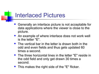
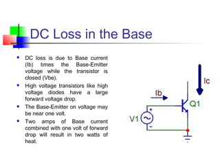
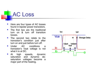
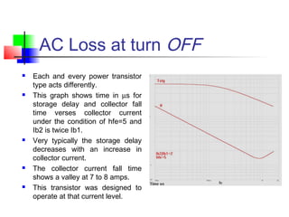
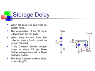
Downloaded 76 times


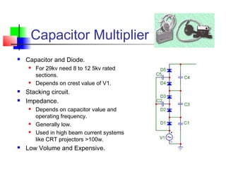
![Vertical Linearity
Vertical linearity is achieved by
adjusting the vertical ramp's slope
many times down the screen.
The VSHAPE DAC has an A.C. wave
form on it that modifies the slope of
the ramp to cause linearity
corrections.
At the maximum vertical frequency
and with the [vertical shape at vertical
frequency maximum] set to a value
that causes a 4 volt p-p signal on the
VSHAPE DAC set R12C for good
linearity.
If the vertical frequency is reduced
then the p-p voltage on the VSHAPE
DAC will reduce. This is set by the
[vertical shape at vertical frequency
minimum] control.](https://image.slidesharecdn.com/8f60e942-e3e5-4bc4-842b-f5ff65f05067-160112221136/85/3-_CRT-Display-Design_A_-40-320.jpg)


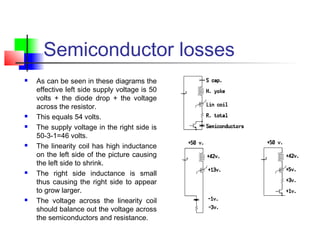


This document discusses the design of CRT displays, including deflection and high voltage systems. It covers scanning methods, deflection principles using magnetic coils, and types of displays like stroke and raster. Vertical and horizontal deflection circuits are described, along with high voltage flyback systems. Details are provided on vertical deflection principles, power amplifiers, retrace boosters, centering, and ramp generators.


