1. 1
ABSTRACT
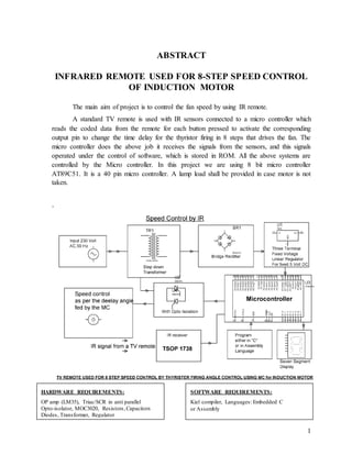
INFRARED REMOTE USED FOR 8-STEP SPEED CONTROL
OF INDUCTION MOTOR
The main aim of project is to control the fan speed by using IR remote.
A standard TV remote is used with IR sensors connected to a micro controller which
reads the coded data from the remote for each button pressed to activate the corresponding
output pin to change the time delay for the thyristor firing in 8 steps that drives the fan. The
micro controller does the above job it receives the signals from the sensors, and this signals
operated under the control of software, which is stored in ROM. All the above systems are
controlled by the Micro controller. In this project we are using 8 bit micro controller
AT89C51. It is a 40 pin micro controller. A lamp load shall be provided in case motor is not
taken.
.
HARDWARE REQUIREMENTS:
OP amp (LM35), Triac/SCR in anti parallel
Opto-isolator, MOC3020, Resistors,Capacitors
Diodes, Transformer, Regulator
SOFTWARE REQUIREMENTS:
Kiel compiler, Languages: Embedded C
or Assembly
2. 1
WORKING PROCEDURE
In this project the firing angle or pulse to gate of the thyristors is controlled by the
push buttons. Load is connected to supply in series with anti parallel of SCRs. These SCRs
are interfaced to the micro controller through the opto isolator.
A standard TV remote is used with IR sensors connected to a micro controller which
reads the coded data from the remote for each button pressed to activate the corresponding
output pin to change the time delay for the thyristor firing in 8 steps that drives the fan. A
TSOP is connected microcontroller to collect the data from TV remote. When one of the
button on TV remote is pressed then pulse to gate is delayed by 2msec by the micro
controller. If one of the other button on TV remote is pressed then the pulse is delayed by a
4msec. So by pressing buttons on TV the motor runs at different speed In this way the speed
control of induction motor is achieved by anti parallel connection of two SCRs.
REGULATED POWER SUPPLY
In a typical linear power supply, AC line voltage is first down-converted to a
smaller peak voltage using a transformer which is then rectified using a full wave bridge
3. 1
rectifier circuit. A capacitor filter is then used to smoothen the obtained sinusoidal signal.
The residual periodic variation or ripple in this filtered signal is eliminated using an active
regulator.
To obtain a DC power supply with both positive and negative output voltages, a
center-tapped transformer is used, where a third wire is attached to the middle of the
secondary winding and it is taken as the common ground point. Then voltages from the
opposite ends of the winding will be positive or negative with respect to this point.
BLOCK DIAGRAM OF A REGULATED POWER SUPPLY
The regulated DC output is very smooth with no ripple. It is suitable for all electronic
circuits.
TRANSFORMER
Transformers convert AC electricity from one voltage to another with little loss of
power. Transformers work only with AC and this is one of the reasons why mains electricity
is AC.
Transformer circuit symbol
4. 1
Step-up transformers increase voltage, step-down transformers reduce voltage.
Most power supplies use a step-down transformer to reduce the dangerously high mains
voltage (230V in UK) to a safer low voltage.
The input coil is called the primary and the output coil is called the secondary.
There is no electrical connection between the two coils, instead they are linked by an
alternating magnetic field created in the soft-iron core of the transformer. The two lines in the
middle of the circuit symbol represent the core.
Transformers waste very little power so the power out is (almost) equal to the
power in. Note that as voltage is stepped down current is stepped up.
The ratio of the number of turns on each coil, called the turns ratio,
determines the ratio of the voltages. A step-down transformer has a large number of turns on
its primary (input) coil which is connected to the high voltage mains supply, and a small
number of turns on its secondary (output) coil to give a low output voltage.
Vp = primary (input) voltage
Np = number of turns on primary coil
Ip = primary (input) current
Vs = secondary (output) voltage
Ns = number of turns on secondary coil
Is = secondary (output) current
RECTIFIER
There are several ways of connecting diodes to make a rectifier to convert AC to
DC. The bridge rectifier is the most important and it produces full-wave varying DC. A full-
wave rectifier can also be made from just two diodes if a centre-tap transformer is used, but
this method is rarely used now that diodes are cheaper. A single diode can be used as a
rectifier but it only uses the positive (+) parts of the AC wave to produce half-wave varying
DC.
BRIDGE RECTIFIER
5. 1
A bridge rectifier can be made using four individual diodes, but it is also available in special
packages containing the four diodes required. It is called a full-wave rectifier because it uses
the entire AC wave (both positive and negative sections). 1.4V is used up in the bridge
rectifier because each diode uses 0.7V when conducting and there are always two diodes
conducting, as shown in the diagram below. Bridge rectifiers are rated by the maximum
current they can pass and the maximum reverse voltage they can withstand (this must be at
least three times the supply RMS voltage so the rectifier can withstand the peak voltages).
Please see the Diodes page for more details, including pictures of bridge rectifiers.
Output: full-wave varying DC
(Using all the AC wave)
Bridge rectifier
Alternate pairs of diodes conduct, changing over the connections so the alternating directions
of AC are converted to the one direction of DC.
SINGLE DIODE RECTIFIER
A single diode can be used as a rectifier but this produces half-wave varying DC
which has gaps when the AC is negative. It is hard to smooth this sufficiently well to supply
electronic circuits unless they require a very small current so the smoothing capacitor does
not significantly discharge during the gaps. Please see the Diodes page for some examples of
rectifier diodes.
6. 1
Single diode rectifier
Output: half-wave varying DC
(Using only half the AC wave)
SMOOTHING
Smoothing is performed by a large value electrolytic capacitor connected across
the DC supply to act as a reservoir, supplying current to the output when the varying DC
voltage from the rectifier is falling. The diagram shows the unsmoothed varying DC (dotted
line) and the smoothed DC (solid line). The capacitor charges quickly near the peak of the
varying DC, and then discharges as it supplies current to the output.
Note that smoothing significantly increases the average DC voltage to almost the
peak value (1.4 × RMS value). For example 6V RMS AC is rectified to full wave DC of
about 4.6V RMS (1.4V is lost in the bridge rectifier), with smoothing this increases to almost
the peak value giving 1.4 × 4.6 = 6.4V smooth DC.
Smoothing is not perfect due to the capacitor voltage falling a little as it
discharges, giving a small ripple voltage. For many circuits a ripple which is 10% of the
supply voltage is satisfactory and the equation below gives the required value for the
smoothing capacitor. A larger capacitor will give less ripple. The capacitor value must be
doubled when smoothing half-wave DC.
7. 1
C = smoothing capacitance in farads (F)
Io = output current from the supply in amps (A)
Vs = supply voltage in volts (V), this is the peak value of the unsmoothed DC
f = frequency of the AC supply in hertz (Hz), 50Hz in the UK
REGULATOR
Voltage regulator ICs are available with fixed (typically 5, 12 and 15V) or
variable output voltages. They are also rated by the maximum current they can pass.
Negative voltage regulators are available, mainly for use in dual supplies. Most regulators
include some automatic protection from excessive current ('overload protection') and
overheating ('thermal protection').
Many of the fixed voltage regulators ICs have 3 leads and look like power transistors, such as
the 7805 +5V 1A regulator shown on the right. They include a hole for attaching a heatsink if
necessary.
8. 1
MICRO CONTROLLER AT89C51
DESCRIPTION
The AT89C51 is a low-power, high-performance CMOS 8-bit
microcomputer with 4K bytes of Flash programmable and erasable read only memory
(PEROM). The device Flash is manufactured using Atmel’s high-density nonvolatile
memory technology and is compatible with the industry-standard MCS-51 instruction set and
pin out. The on-chip Flash allows the program memory to be reprogrammed in-system or by
a conventional nonvolatile memory programmer. By combining a versatile 8-bit CPU with
Flash AT89C51 on a monolithic chip, the Atmel AT89C51 is a powerful microcomputer
which provides a highly-flexible and cost-effective solution to many embedded control
applications.
The AT89C51 provides the following standard features: 4K bytes of Flash, 128
bytes of RAM, 32 I/O lines, two 16-bit timer/counters, five vector two-level interrupt
architecture, a full duplex serial port, and on-chip oscillator and clock circuitry. In addition,
the AT89C51 is designed with static logic for operation down to zero frequency and
supports two software selectable power saving modes. The Idle Mode stops the CPU
while allowing the RAM, timer/counters, serial port and interrupt system to continue
functioning. The power-down Mode saves the RAM contents but freezes the oscillator
11. 1
PIN DESCRIPTION
VCC: Supply voltage.
GND: Ground.
Port 0
Port 0 is an 8-bit open-drain bi-directional I/O port. As an output port, each pin
can sink eight TTL inputs. When 1s are written to port 0 pins, the pins can be used as
high- impedance inputs. Port0 may also be configured to be the multiplexed low-order
address/data bus during accesses to external program and data memory. In this mode
P0 has internal pull-ups. Port0 also receives the code bytes during flash programming, and
outputs the code bytes during program verification. External pull-ups are required
during program verification.
Port 1
Port 1 is an 8-bit bi-directional I/O port with internal pull-ups. The Port 1
output buffers can sink/source four TTL inputs. When 1s are written to Port 1 pins
they are pulled high by the internal pull-ups and can be used as inputs. As inputs,
Port 1 pins that are externally being pulled low will source current (IIL) because of
the internal pull-ups. Port 1 also receives the low-order address bytes during
Flash programming and verification.
Port 2
Port 2 is an 8-bit bi-directional I/O port with internal pull-ups. The Port 2 output
buffers can sink/source four TTL inputs. When 1s are written to Port 2 pins they are pulled
high by the internal pull-ups and can be used as inputs. As inputs, Port 2 pins that are
externally being pulled low will source current (IIL) because of the internal pull-ups. Port 2
emits the high-order address byte during fetches from external program memory and
during accesses to external data memory that uses 16-bit addresses (MOVX @ DPTR). In
this application, it uses strong internal pull-ups when emitting 1s. During accesses to
external data memory that uses 8-bit addresses (MOVX @ RI), Port 2 emits the contents of the
P2 Special Function Register. Port2 also receives the high- order address bits and some
control signals during flash programming and verification.
Port 3
12. 1
Port 3 is an 8-bit bi-directional I/O port with internal pull-ups. The Port 3 output
buffers can sink/source four TTL inputs. When 1s are written to Port 3 pins they are
pulled high by the internal pull-ups and can be used as inputs. As inputs, Port 3 pins
that are externally being pulled low will source current (IIL) because of the pull-ups.
Port 3 also serves the functions of various special features of the AT89C51 as listed.
Port3 also receives some control signals for Flash programming and verification.
RST
Reset input. A high on this pin for two machine cycles while the oscillator
is running resets the device.
ALE/PROG
Address Latch Enable output pulse for latching the low byte of the address during
accesses to external memory. This pin is also the program pulse input (PROG) during Flash
programming. In normal operation ALE is emitted at a constant rate of 1/6 the oscillator
frequency, and may be used for external timing or clocking purposes. Note, however, that
one ALE pulse is skipped during each access to external Data Memory. If desired, ALE
operation can be disabled by setting bit 0 of SFR location 8EH. With the bit set, ALE is active
only during a MOVX or MOVC instruction. Otherwise, the pin is weakly pulled high.
Setting the ALE disable bit has no effect if the microcontroller is in external execution
mode.
PSEN
Program Store Enable is the read strobe to external program memory. When the
Port Pin Alternate Functions
P3.0 RXD (serial input port)
P3.1 TXD (serial output port)
P3.2 INT0 (external interrupt 0)
P3.3 INT1 (external interrupt 1)
P3.4 T0 (timer 0 external input).
P3.5 T1 (timer 1 external input).
P3.6 WR (external data memory write
strobe).
P3.7 RD (external data memory read strobe).
13. 1
AT89C51 is executing code from external program memory, PSEN is activated twice
each machine cycle, except that two PSEN activations are skipped during each access to
external data memory.
EA/VPP
External access enable. EA must be strapped to GND in order to enable the
device to fetch code from external program memory locations starting at 0000H up to
FFFFH. Note, however, that if lock bit 1 is programmed, EA will be internally latched on
reset. EA should be strapped to VCC for internal program executions. This pin also
receives the 12-volt programming enable voltage (VPP) during Flash programming, for parts
that require 12-volt VPP.
XTAL1
Input to the inverting oscillator amplifier and input to the internal clock operating circuit.
XTAL2
Output from the inverting oscillator amplifier.
OscillatorCharacteristics
XTAL1 and XTAL2 are the input and output, respectively, of an inverting amplifier which
can be configured for use as an on-chip oscillator, as shown in Figure1. Either a quartz crystal
or ceramic resonant or may be used. To drive the device from an external clock source,
XTAL2 should be left unconnected while XTAL1 is driven as shown in Figure 2.There are no
requirements on the duty cycle of the external clock signal, since the input to the internal
clocking circuitry is through a divide-by-two flip-flop, but minimum and maximum voltage
high and low time specifications must be observed.
Idle Mode
In idle mode, the CPU puts itself to sleep while all the on-chip peripherals
remain active. The mode is invoked by software. The content of the on-chip RAM and
all the special functions registers remain unchanged during this mode. The idle
mode can be terminated by any enabled interrupt or by a hardware reset. It should be
noted that when idle is terminated by a hardware reset, the device normally resumes
program execution, from where it left off, up to two machine cycles before the internal
reset algorithm takes control. On-chip hardware inhibits access to internal RAM in this
event, but access to the port pins is not inhibited. To eliminate the possibility of an
unexpected write to a port pin when Idle is terminated by reset, the instruction following
14. 1
the one that invokes Idle should not be one that writes to a port pin or to external
memory.
Status ofExternalPins during Idle andPower-downModes
Power-down Mode
In the power-down mode, the oscillator is stopped, and the instruction that
invokes power-down is the last instruction executed. The on-chip RAM and Special
Function Registers retain their values until the power-down mode is terminated. The
only exit from power-down is a hardware reset. Reset redefines the SFRs but does not
change the on-chip RAM. The reset should not be activated before VCC is restored to its
normal operating level and must be held active long enough to allow the oscillator to
restart and stabilize.
Program Memory Lock Bits
On the chip are three lock bits which can be left
unprogrammed (U) or can be programmed (P) to obtain the additional features listed
in the table below. When lock bit 1 is programmed, the logic level at the EA pin is
sampled and latched during reset. If the device is powered up without a reset, the latch
initializes to a random value, and holds that value until reset is activated. It is necessary
that the latched value of EA be in agreement with the current logic level at that pin in
order for the device to function properly.
Mode
Program
Memory
ALE PSEN PORT0 PORT1 PORT2 PORT3
Idle Internal 1 1 Data Data Data Data
Idle External 1 1 Float Data Address Data
Power-
down
Internal 0 0 Data Data Data Data
Power-
down
External 0 0 Float Data Data Data
15. 1
Lock Bit Protection Modes
Program Lock
Bits
LB1
LB2 LB3 Protection Type
1 U U U No program lock features.
2 P U U MOVC instructions executed from external program
memory are
disabled from fetching code bytes from internal
memory, EA is
sampled and latched on reset and further
programming of the Flash
is disabled
3 P P U Same as mode 2, also verify is disabled
4 P P P Same as mode 3, also external execution is disabled
Programming the Flash
VPP= 12V VPP = 5V
Top-side Mark AT89C51
xxxx
AT89C51
xxxx-5
16. 1
The
AT89C51 is normally shipped with the on-chip Flash memory array in the erased state
(that is, contents = FFH) and ready to be programmed. The programming interface accepts
either a high-voltage (12-volt) or a low-voltage (VCC) program enable signal. The low-
voltage programming mode provides a convenient way to program the AT89C51 inside
the user’s system, while the high-voltage programming mode is compatible with
conventional third-party Flash or EPROM programmers the AT89C51 is shipped with
either the high-voltage or low-voltage programming mode enabled. The respective top-
side marking and device signature codes are listed in the following table.
The AT89C51 code memory array is programmed byte-by-byte in either
programming mode. To program any non-blank byte in the on-chip Flash Memory, the
entire memory must be erased using the Chip Erase Mode.
Programming Algorithm
Before programming the AT89C51, the address, data and control signals
should be set up according to the Flash programming mode table and Figure 3 and Figure 4.
To program the AT89C51, take the following steps:
1. Input the desired memory location on the address lines.
2. Input the appropriate data byte on the data lines.
3. Activate the correct combination of control signals.
yyww yyww
Signature
(030H) = 1EH
(031H) = 51H
(032H) =F FH
(030H) = 1EH
(031H) = 51H
(032H) = 05H
17. 1
4. Raise EA/VPP to 12V for the high-voltage programming mode.
5. Pulse ALE/PROG once to program a byte in the flash array or the lock bits. The byte
Write cycle is self-timed and typically takes no more than 1.5 Ms.
Repeat steps 1 through 5, changing the address and data for the entire array or
until the end of the object file is reached.
Data Polling
The AT89C51 features Data Polling to indicate the end of a write cycle. During a
write cycle, an attempted read of the last byte written will result in the complement of the
written datum on PO.7. Once the write cycle has been completed, true data are valid on all
outputs, and the next cycle may begin. Data Polling may begin any time after a write cycle has
been initiated. Ready/Busy: The progress of byte programming can also be monitored by the
RDY/BSY output signal. P3.4 is pulled low after ALE goes high during programming to
indicate BUSY. P3. 4 are pulled high again when programming is done to indicate
READY.
Program Verify
If lock bits LB1 and LB2 have not been programmed, the programmed
code data can be read back via the address and data lines for verification. The lock bits
cannot be verified directly. Verification of the lock bits is achieved by observing that
their features are enabled.
Chip Erase
The entire Flash array is erased electrically by using the proper combination of
control signals and by holding ALE/PROG low for 10 ms. The code array is written with
all “1”s. The chip erase operation must be executed before the code memory can be re-
programmed.
Reading the Signature Bytes
The signature bytes are read by the same procedure as a normal
verification of locations 030H, 0 31H, and 0 32H, except that P3.6 and
P3.7 must be pulled to a logic low. The values returned are as follows.
(030H) = 1EH indicates manufactured by Atmel
(031H) = 51H indicates 89C51
(032H) = FFH indicates 12V programming
(032H) = 05H indicates 5V programming
Programming Interface
Every code byte in the flash array can be written and the entire array can
18. 1
be erased by using the appropriate combination of control signals. The write operation
cycle is self-timed and once initiated, will automatically time itself to completion. All
major programming vendors offer world wide support for the Atmel microcontroller
series. Please contact your local programming vendor for the appropriate software
revision.
Zero Crossing Detectors and Comparators
Introduction
Zero crossing detectors as a group are not a well-understood application, although
they are essential elements in a wide range of products. It has probably escaped the notice of
readers who have looked at the lighting controller and the Linkwitz Cosine Burst Generator,
but both of these rely on a zero crossing detector for their operation.
A zero crossing detector literally detects the transition of a signal waveform from
positive and negative, ideally providing a narrow pulse that coincides exactly with the zero
voltage condition. At first glance, this would appear to be an easy enough task, but in fact it
is quite complex, especially where high frequencies are involved. In this instance, even 1
kHz starts to present a real challenge if extreme accuracy is needed.
The not so humble comparator plays a vital role - without it, most precision zero crossing
detectors would not work, and we'd be without digital audio, PWM and a multitude of other
applications taken for granted.
Basic Low Frequency Circuit
Figure 1 shows the zero crossing detectors are used for the dimmer ramp generator
in Project 62. This circuit has been around (almost) forever, and it does work reasonably
well. Although it has almost zero phase inaccuracy, that is largely because the pulse is so
broad that any inaccuracy is completely swamped. The comparator function is handled by
transistor Q1 - very basic, but adequate for the job.
The circuit is also sensitive to level, and for acceptable performance the AC
waveform needs to be of reasonably high amplitude. 12-15V AC is typical. If the voltage is
too low, the pulse width will increase. The arrangement shown actually gives better
performance than the version shown in Project 62 and elsewhere on the Net. In case you
19. 1
were wondering, R1 is there to ensure that the voltage falls to zero - stray capacitance is
sufficient to stop the circuit from working without it.
Figure 1 - Basic 50/60Hz Zero Crossing Detector
The pulse width of this circuit (at 50Hz) is typically around 600us (0.6ms) which
sounds fast enough. The problem is that at 50Hz each half cycle takes only 10ms (8.33ms at
60Hz), so the pulse width is over 5% of the total period. This is why most dimmers can only
claim a range of 10%-90% - the zero crossing pulse lasts too long to allow more range.
While this is not a problem with the average dimmer, it is not acceptable for
precision applications. For a tone burst generator (either the cosine burst or a 'conventional'
tone burst generator), any inaccuracy will cause the switched waveform to contain glitches.
The seriousness of this depends on the application.
Precision zero crossing detectors come in a fairly wide range of topologies, some interesting,
others not. One of the most common is shown in Project 58, and is commonly used for this
application. The exclusive OR (or XOR) gate makes an excellent edge detector, as shown in
Figure 2.
20. 1
Figure 2 - Exclusive OR Gate Edge Detector
There is no doubt that the circuit shown above is more than capable of excellent
results up to quite respectable frequencies. The upper frequency is limited only by the speed
of the device used, and with a 74HC86 it has a propagation delay of only 11ns [1], so
operation at 100 kHz or above is achievable.
The XOR gate is a special case in logic. It will output a 1 only when the inputs are
different (i.e. one input must be at logic high (1) and the other at logic low (0v). The resistor
and cap form a delay so that when an edge is presented (either rising or falling), the delayed
input holds its previous value for a short time. In the example shown, the pulse width is 50ns.
The signal is delayed by the propagation time of the device itself (around 11ns), so a small
phase error has been introduced. The rise and fall time of the square wave signal applied was
50ns, and this adds some more phase shift.
There is a pattern emerging in this article - the biggest limitation is speed, even for
relatively slow signals. While digital logic can operate at very high speeds, we have well
reached the point where the signals can no longer be referred to as '1' and '0' - digital signals
are back into the analogue domain, specifically RF technology.
The next challenge we face is converting the input waveform (we will assume a sine
wave ) into sharply defined edges so the XOR can work its magic. Another terribly under-
rated building block is the comparator. While opamps can be used for low speed operation
(and depending on the application), extreme speed is needed for accurate digitization of an
analogue signal. It may not appear so at first glance, but a zero crossing detector is a special
purpose analogue to digital converter (ADC).
21. 1
Comparators
The comparator used for a high speed zero crossing detectors, a PWM converter or
conventional ADC is critical. Low propagation delay and extremely fast operation are not
only desirable, they are essential.
Comparators may be the most underrated and under utilized monolithic linear
component. This is unfortunate because comparators are one of the most flexible and
universally applicable components available. In large measure the lack of recognition is due
to the IC opamp, whose versatility allows it to dominate the analog design world.
Comparators are frequently perceived as devices that crudely express analog signals in digital
form - a 1-bit A/D converter. Strictly speaking, this viewpoint is correct. It is also wastefully
constrictive in its outlook. Comparators don't “just compare” in the same way that opamps
don't "just amplify". The above quote was so perfect that I just had to include it. Comparators
are indeed underrated as a building block, and they have two chief requirements ... low input
offset and speed. For the application at hand (a zero crossing detector), both of these factors
will determine the final accuracy of the circuit. The XOR has been demonstrated to give a
precise and repeatable pulse, but its accuracy depends upon the exact time it 'sees' the
transition of the AC waveform across zero. This task belongs to the comparator.
Figure 3 - Comparator Zero Crossing Detector
In Figure 3 we see a typical comparator used for this application. The output is a
square wave, which is then sent to a circuit such as that in Figure 2. This will create a single
pulse for each square wave transition, and this equates to the zero crossings of the input
signal. It is assumed for this application that the input waveform is referenced to zero volts,
so swings equally above and below zero.
22. 1
Figure 4 - Comparator Timing Error
Figure 4 shows how the comparator can mess with our signal, causing the transition to
be displaced in time, thereby causing an error. The significance of the error depends entirely
on our expectations - there is no point trying to get an error of less than 10ns for a dimmer,
for example.
The LM339 comparator that was used for the simulation is a very basic type indeed, and
with a quoted response time of 300ns it is much too slow to be usable in this application.
This is made a great deal worse by the propagation delay, which (as simulated) is 1.5us. In
general, the lower the power dissipation of a comparator, the slower it will be, although
modern IC techniques have overcome this to some extent.
We can see that the zero crossing of the sine wave (shown in green) occurs well before
the output (red) transition - the cursor positions are set for the exact zero crossing of each
signal. The output transition starts as the input passes through zero, but because of device
delays, the output transition is almost 5us later. Most of this delay is caused by the rather
leisurely pace at which the output changes - in this case, about 5us for the total 7V peak to
peak swing. That gives us a slew rate of 1.4V/us which is useless for anything above 100Hz
or so.
One of the critical factors with the comparator is its supply voltage. Ideally, this should
be as low as possible, typically with no more than ±5V. The higher the supply voltage, the
further the output voltage has to swing to get from maximum negative to maximum positive
and vice versa. While a slew rate of 100V/us may seem high, that is much too slow for an
accurate ADC, pulse width modulator or zero crossing detectors.
23. 1
At 100V/us and a total supply voltage of 10V (±5V), it will take 0.1us (100ns) for the
output to swing from one extreme to the other. To get that into the realm of what we need,
the slew rate would need to be 1kV/us, giving a 10ns transition time. Working from Figure 3,
you can see that even then there is an additional timing error of 5ns - not large, and in reality
probably as good as we can expect.
The problem is that the output doesn't even start to change until the input voltage passes
through the reference point (usually ground). If there is any delay caused by slew rate
limiting, by the time the output voltage passes through zero volts, it is already many
nanoseconds late. Extremely high slew rates are possible, and Reference 2 has details of a
comparator that is faster than a TTL inverter! Very careful board layout and attention to
bypassing is essential at such speeds, or the performance will be worse than woeful.
LIQUID CRYSTAL DISPLAY (LCD)
Description
This is the first interfacing example for the Parallel Port. We will start with something
simple. This example doesn't use the Bi-directional feature found on newer ports, thus it
should work with most, if no all Parallel Ports. It however doesn't show the use of the Status
Port as an input. So what are we interfacing? A 16 Character x 2 Line LCD Module to the
Parallel Port. These LCD Modules are very common these days, and are quite simple to work
with, as all the logic is required to run them is on board.
LCD Background
Frequently, an 8051 program must interact with the outside world using input and
output devices that communicate directly with a human being. One of the most common
devices attached to an 8051 is an LCD display. Some of the most common LCDs connected
to the 8051 are 16x2 and 20x2 displays. This means 16 characters per line by 2 lines and 20
characters per line by 2 lines, respectively.
Fortunately, a very popular standard exists which allows us to communicate with the
vast majority of LCDs regardless of their manufacturer. The standard is referred to as
HD44780U, which refers to the controller chip which receives data from an external source
(in this case, the 8051) and communicates directly with the LCD.
24. 1
44780 LCD BACKGROUND
The 44780 standard requires 3 control lines as well as either 4 or 8 I/O lines for the
data bus. The user may select whether the LCD is to operate with a 4-bit data bus or an 8-bit
data bus. If a 4-bit data bus is used the LCD will require a total of 7 data lines (3 control lines
plus the 4 lines for the data bus). If an 8-bit data bus is used the LCD will require a total of
11 data lines (3 control lines plus the 8 lines for the data bus).
The three control lines are referred to as EN, RS, and RW.
The EN line is called "Enable." This control line is used to tell the LCD that you are
sending it data. To send data to the LCD, your program should make sure this line is low (0)
and then set the other two control lines and/or put data on the data bus. When the other lines
are completely ready, bring EN high (1) and wait for the minimum amount of time required
by the LCD datasheet (this varies from LCD to LCD), and end by bringing it low (0) again.
The RS line is the "Register Select" line. When RS is low (0), the data is to be treated as
a command or special instruction (such as clear screen, position cursor, etc.). When RS is
high (1), the data being sent is text data which should be displayed on the screen. For
example, to display the letter "T" on the screen you would set RS high.
The RW line is the "Read/Write" control line. When RW is low (0), the information on
the data bus is being written to the LCD. When RW is high (1), the program is effectively
querying (or reading) the LCD. Only one instruction ("Get LCD status") is a read command.
All others are write commands--so RW will almost always be low. Finally, the data bus
consists of 4 or 8 lines (depending on the mode of operation selected by the user). In the case
of an 8-bit data bus, the lines are referred to as DB0, DB1, DB2, DB3, DB4, DB5, DB6, and
DB7.
26. 1
If you want backlight than connect pin 15 of LCD to 5V and pin 16 of LCD to GND. By
adjusting 10k resistor make pin 3 of LCD at 0V. If connection is proper you will see this
after power on.
Pin Information of LCD:
Algorithm to send data to LCD:
1. Make R/W low
2. Make RS=0; if data byte is command
RS=1; if data byte is data (ASCII value)
3. Place data byte on data register
4. Pulse E (HIGH to LOW)
5. Repeat the steps to send another data byte
27. 1
LCD Initialization:
This is the pit fall for beginners. Proper working of LCD depend on the how the LCD is
initialized. We have to send few command bytes to initialize the lcd. Simple steps to
initialize the LCD
1. Specify function set:
Send 38H for 8-bit, double line and 5x7 dot character format.
2. Display On-Off control:
Send 0FH for display and blink cursor on.
3. Entry mode set:
Send 06H for cursor in increment position and shift is invisible.
4. Clear display:
Send 01H to clear display and return cursor to home position.
Opto-Isolator
An opto-isolator integrated circuit. The "MB 111", manufactured by RFT ("Rundfunk-
und Fernmelde-Technik"), contains an infrared LED and silicon photodiode with an
integrated amplifier stage. This article is about the electronic component. For the optical
component, see optical isolator.
In electronics, an opto-isolator (or optical isolator, optocoupler, photocoupler, or
photoMOS) is a device that uses a short optical transmission path to transfer a signal between
elements of a circuit, typically a transmitter and a receiver, while keeping them electrically
isolated — since the signal goes from an electrical signal to an optical signal back to an
electrical signal, electrical contact along the path is broken.
The opto-isolator is simply a package that contains both an infrared LED and a
photodetector such as silicon diode, transistor Darlington pair, or SCR. The wave-length
response of each device is tailored to be as identical as possible to permit the highest measure
of coupling possible.
1 Configuration
2 Applications
28. 1
Configurations
Schematic diagram of a very simple opto-isolator with an LED and phototransistor.
The dashed line represents the isolation barrier, over which no electrical contact can be
permitted.
A common implementation involves a LED and a phototransistor, separated so that light
may travel across a barrier but electrical current may not. When an electrical signal is applied
to the input of the opto-isolator, its LED lights, its light sensor then activates, and a
corresponding electrical signal is generated at the output. Unlike a transformer, the opto-
isolator allows for DC coupling and generally provides significant protection from serious
over voltage conditions in one circuit affecting the other.
With a photodiode as the detector, the output current is proportional to the amount of incident
light supplied by the emitter. The diode can be used in a photovoltaic mode or a
photoconductive mode.
In photovoltaic mode, the diode acts like a current source in parallel with a forward-biased
diode. The output current and voltage are dependent on the load impedance and light
intensity.
In photoconductive mode, the diode is connected to a supply voltage, and the magnitude of
the current conducted is directly proportional to the intensity of light.
The optical path may be air or a dielectric waveguide. The transmitting and receiving
elements of an optical isolator may be contained within a single compact module, for
mounting, for example, on a circuit board; in this case, the module is often called an
optoisolator or opto-isolator. The photo sensor may be a photocell, phototransistor, or an
optically triggered SCR or TRIAC. Occasionally, this device will in turn operate a power
relay or contactor.
29. 1
For analog isolation, special "analog" optoisolators are used. These devices have two
independent, closely matched phototransistors, one of which is typically used to linearize the
response using negative feedback.
Application
A simple circuit with an opto-isolator. When switch S1 is closed, LED D1 lights, which
trigger phototransistor Q1, which pulls the output pin low. This circuit, thus, acts as a
NOT gate.
Among other applications, opto-isolators can help cut down on ground loops, block
voltage spikes, and provide electrical isolation.
One of the requirements of the MIDI (Musical Instrument Digital Interface) standard is that
input connections be opto-isolated.
They are used to isolate low-current control or signal circuitry from transients generated or
transmitted by power supply and high-current control circuits. The latter are used within
motor and machine control function blocks.
Most switched-mode power supplies utilize optocouplers for mains isolation.
30. 1
KEIL SOFTWARE
INTRODUCTION
An assembler is a software tool designed to simplify the task of writing computer
programs. It translates symbolic code into executable object code. This object code may then
be programmed into a microcontroller and executed. Assembly language programs translate
directly into CPU instructions which instruct the processor what operations to perform.
Therefore, to effectively write assembly programs, you should be familiar with both the
microcomputer architecture and the assembly language.
Assembly language operation codes (mnemonics) are easily remembered. You can also
symbolically express addresses and values referenced in the operand field of instructions.
Since you assign these names, you can make them as meaningful as the mnemonics for the
instructions. For example, if your program must manipulate a date as data, you can assign it
the symbolic name DATE. If your program contains a set of instructions used as a timing
loop (a set of instructions executed repeatedly until a specific amount of time has passed),
you can name the instruction group TIMER_LOOP.
An assembly program has three constituent parts:
1. Machine instructions
2. Assembler directives
3. Assembler controls
A machine instruction is a machine code that can be executed by the machine. Detailed
discussion of the machine instructions can be found in the hardware manuals of the 8051 or
derivative microcontroller.
Assembler directives are used to define the program structure and symbols, and generate
non-executable code (data, messages, etc.). Assembler directives instruct the assembler how
to process subsequent assembly language instructions. Directives also provide a way for you
to define program constants and reserve space for variables.
Assembler controls set the assembly modes and direct the assembly flow. Assembler
controls direct the operation of the assembler when generating a listing file or object file.
Typically, controls do not impact the code that is generated by the assembler. Controls can be
specified on the command line or within an assembler source file.
DIRECTIVE CATEGORIES
The Ax51 assembler has several directives that permit you to define symbol values,
reserve and initialize storage, and control the placement of your code. The directives should
not be confused with instructions. They do not produce executable code, and with the
31. 1
exception of the DB, DW and DD directives, they have no direct effect on the contents of
code memory. These directives change the state of the assembler, define user symbols, and
add information to the object file. The following table provides an overview of the assembler
directives. Page refers to the page number in this user’s guide where you can find detailed
information about the directive.
Directive / Page Format Description
BIT 114 symbols BIT address Define a bit address in bit data space.
BSEG 111 BSEG [AT absolute address] Define an absolute segment within the
Bit address space.
CODE 114 symbols CODE code address Assign a symbol name to a specific
Address in the code space.
CSEG 111 CSEG [AT absolute address] Define an absolute segment within the
Code address space.
DATA 114 symbol DATA data address assign a symbol name to a specific
On-chip data address.
DB 119 [label:] DB expression [, expr ...] Generate a list of byte values.
DBIT 122 [label:] DBIT expression Reserve a space in bit units.
DD 121 [label:] DD expression [, expr ...] Generate a list of double word values.
DS 123 [label:] DS expression Reserve space in byte units.
DSB 124 [label:] DSB expression Reserve space in byte units.
DSD 126 [label:] DSD expression Reserve space in double word units.
DSEG 111 DSEG [AT absolute address] Define an absolute segment within the
Indirect internal data space.
Shaded directives and options are available only in AX51 and A251.
DSW 125 [label:] DSW expression Reserve space in word units;
Advances the location counter of the current segment.
DW 120 [label:] DW expression [, expr. ...] Generate a list of word values.
END 136 END Indicate end of program.
EQU 113 EQU expression Set symbol value permanently.
EVEN 134 EVEN Ensure word alignment for variables.
EXTRN 131
EXTERN EXTRN class [: type] (symbol [...])
Defines symbols referenced in the current module that are defined in other modules. .
CONCLUSIONS
IDATA 114 symbol IDATA idata_address Assign a symbol name to a specific indirect
internal address.
ISEG 111 ISEG [AT absolute address] Define an absolute segment within the internal data
space.
LABEL 129 name [:] LABEL [type] Assign a symbol name to an address location within a
segment.
32. 1
LIT 116 symbol LIT ’literal string’ Assign a symbol name to a string.
NAME 132 NAME module name Specify the name of the current module.
ORG 133 ORG expression Set the location counter of the current segment.
PROC 127
ENDP name PROC [type] name ENDP
Define a function start and end.
PUBLIC 130 PUBLIC symbol [, symbol...] Identify symbols which can be used outside the
current module.
RSEG 110 RSEG seg Select a relocatable segment.
SEGMENT 106 seg SEGMENT class [reloctype][alloctype]
Define a relocatable segment.
SET 113 SET expression Set symbol value temporarily.
sfr, 116
sfr16
sbit sfr symbol = address;
sfr16 symbol = address;
Sbit symbol = address;
Define a special function register(SFR) symbol or a SFR bit symbol.
USING 134 USING expressions Set the predefined symbolic register address and reserve
space for the specified register bank.
XDATA 114 symbol XDATA xdata_address assign a symbol name to a specific off-chip
data address.
XSEG 111 XSEG [AT absolute address] Define an absolute segment within the external
data address space.
Shaded directives and options are available only in AX51 and A251.
4The directives are divided into the following categories:
_ Segment Control
Generic Segments: SEGMENT, RSEG
Absolute Segments: CSEG, DSEG, BSEG, ISEG, XSEG
_ Symbol Definition
Generic Symbols: EQU, SET
Address Symbols: BIT, CODE, DATA, IDATA, XDATA
SFR Symbols: sfr, sfr16, sbit
Text Replacement: LIT
_ Memory Initialization
DB, DW, DD
_ Memory Reservation
DBIT, DS, DSB, DSW, DSD
_ Procedure Declaration
PROC / ENDP, LABEL
33. 1
_ Program Linkage
PUBLIC, EXTRN / EXTERN, NAME
_ Address Control
ORG, EVEN, USING
_ Others
END, _ _ERROR_
LANGUAGE EXTENSIONS
Several new variants of the 8051 extend the code and/or xdata space of the
classic 8051 with address extension registers. The following table shows the memory classes
used for programming the extended 8051 devices. These memory classes are available for
classic 8051 devices when you are using memory banking with the LX51 linker/locater. In
addition to the code banking known from the BL51 linker/locater, the LX51 linker/locator
supports also data banking for Xdata and code areas with standard 8051 devices.
The memory prefixes D: I: X: C: B0: B31: cannot be used at Ax51 assembler level.
The memory prefix is only listed for better understanding. The Lx51 linker/locater and
several Debugging tools, for example the µVision2 Debugger, are using memory prefixes to
34. 1
identify the memory class of the address. If you are using the Dallas 390 contiguous mode
the address space for CODE can be C: 0000 - C: 0xFFFFFF.
CONCLUSIONS
Each line of an assembly program can contain only one control, directive, or
instruction statement. Statements must be contained in exactly one line. Multi– line
statements are not allowed. Statements in x51 assembly programs are not column sensitive.
Controls, directives, and instructions may start in any column. Indentation used in the
programs in this project is done for program clarity and is neither required nor expected by
the assembler. The only exception is that arguments and instruction operands must be
separated from controls, directives, and instructions by at least one space.
All x51 assembly programs must include the END directive. This directive signals
to the assembler that this is the end of the assembly program. Any instructions, directives, or
controls found after the END directive are ignored. The shortest valid assembly program
contains only an END directive.
TRIAC
A TRIAC or TRIode for Alternating Current is an electronic component
approximately equivalent to two silicon-controlled rectifiers (SCRs/thyristors) joined in
inverse parallel (paralleled but with the polarity reversed) and with their gates connected
together. The formal name for a TRIAC is bidirectional triode thyristor. This results in a
bidirectional electronic switch which can conduct current in either direction when it is
triggered (turned on) and thus doesn't have any polarity. It can be triggered by either a
positive or a negative voltage being applied to its gate electrode (with respect to A1,
otherwise known as MT1). Once triggered, the device continues to conduct until the current
through it drops below a certain threshold value, the holding current, such as at the end of a
half-cycle of alternating current (AC) mains power. This makes the TRIAC a very
convenient switch for AC circuits, allowing the control of very large power flows with
milliampere-scale control currents. In addition, applying a trigger pulse at a controllable
point in an AC cycle allows one to control the percentage of current that flows through the
TRIAC to the load (phase control). SCRs are unidirectional (one-way) current devices,
making them useful for controlling DC only. If two SCRs are joined in back-to-back parallel
fashion just like two Shockley diodes were joined together to form a DIAC, we have a new
device known as the TRIAC.
35. 1
The TRIAC SCR equivalent and, SCR schematic symbol
Because individual SCRs are more flexible to use in advanced control systems, these are
more commonly seen in circuits like motor drives; TRIACs are usually seen in simple, low-
power applications like household dimmer switches. A simple lamp dimmer circuit is shown
in Figure, complete with the phase-shifting resistor-capacitor network necessary for after-
peak firing.
TRIAC phase-control of power
TRIACs are notorious for not firing symmetrically. This means these usually won't trigger at
the exact same gate voltage level for one polarity as for the other. Generally speaking, this is
undesirable, because unsymmetrical firing results in a current waveform with a greater
variety of harmonic frequencies. Waveforms that are symmetrical above and below their
average centerlines are comprised of only odd-numbered harmonics. Unsymmetrical
waveforms, on the other hand, contain even-numbered harmonics (which may or may not be
accompanied by odd-numbered harmonics as well).
36. 1
In the interest of reducing total harmonic content in power systems, the fewer and less
diverse the harmonics, the better -- one more reason individual SCRs are favored over
TRIACs for complex, high-power control circuits. One way to make the TRIAC's current
waveform more symmetrical is to use a device external to the TRIAC to time the triggering
pulse. A DIAC placed in series with the gate does a fair job of this is shown in the figure.
DIAC improves symmetry of control
DIAC breakover voltages tend to be much more symmetrical (the same in one polarity as the
other) than TRIAC triggering voltage thresholds. Since the DIAC prevents any gate current
until the triggering voltage has reached a certain, repeatable level in either direction, the
firing point of the TRIAC from one half-cycle to the next tends to be more consistent, and the
waveform more symmetrical above and below its centerline.
Practically all the characteristics and ratings of SCRs apply equally to TRIACs, except that
TRIACs of course are bidirectional (can handle current in both directions). Not much more
needs to be said about this device except for an important caveat concerning its terminal
designations. From the equivalent circuit diagram shown earlier, one might think that main
terminals 1 and 2 were interchangeable. These are not! Although it is helpful to imagine the
TRIAC as being composed of two SCRs joined together, it in fact is constructed from a
single piece of semiconducting material, appropriately doped and layered. The actual
operating characteristics may differ slightly from that of the equivalent model.
This is made most evident by contrasting two simple circuit designs, one that works and one
that doesn't. The following two circuits are a variation of the lamp dimmer circuit shown
earlier, the phase-shifting capacitor and DIAC removed for simplicity's sake. Although the
resulting circuit lacks the fine control ability of the more complex version (with capacitor and
DIAC), it does function is shown in the figure.
37. 1
This circuit with the gate to MT2 does function.
Suppose we were to swap the two main terminals of the TRIAC around. According to the
equivalent circuit diagram shown earlier in this section, the swap should make no difference.
The circuit ought to work
With the gate swapped to MT1, this circuit does not function.
However, if this circuit is built, it will be found that it does not work! The load will receive
no power, the TRIAC refusing to fire at all, no matter how low or high a resistance value the
control resistor is set to. The key to successfully triggering a TRIAC is to make sure the gate
receives its triggering current from the main terminal 2 side of the circuit (the main terminal
on the opposite side of the TRIAC symbol from the gate terminal). Identification of the MT1
and MT2 terminals must be done via the TRIAC's part number with reference to a data sheet
or book.
For higher-powered, more-demanding loads, two SCRs in inverse parallel may be used
instead of one TRIAC. Because each SCR will have an entire half-cycle of reverse polarity
voltage applied to it, turn-off of the SCRs is assured, no matter what the character of the load.
However, due to the separate gates, proper triggering of the SCRs is more complex than
triggering a TRIAC. In addition to commutation, a TRIAC may also not turn on reliably with
non-resistive loads, because due to the phase shift the holding current may not be achievable
at trigger time. To overcome that, pulse trains may be used to repeatedly try to trigger the
TRIAC until it finally turns on. The advantage is that the gate current does not need to be
38. 1
maintained throughout the entire conduction angle, which can be beneficial when there is
only limited drive capability available.
GENERAL DESCRIPTION
Passivated, sensitive gate triacs in a plastic envelope, intended for use in general purpose
bidirectional switching and phase control VDRM Repetitive peak off-state 600 800 V
applications, where high sensitivity is voltages required in all four quadrants.
40. 1
Application
Low power TRIACs are used in many applications such as light dimmers, speed
controls for electric fans and other electric motors, and in the modern computerized control
circuits of many household small and major appliances.
However, when used with inductive loads such as electric fans, care must be taken to assure
that the TRIAC will turn off correctly at the end of each half-cycle of the AC power.
A snubber circuit (usually of the RC type) is often used between A1 and A2 to assist this
turn-off. Snubber circuits are also used to prevent premature triggering, caused for example
by voltage spikes in the mains supply. Also, a gate resistor or capacitor (or both in parallel)
may be connected between gate and A1 to further prevent false triggering. That, however,
increases the required trigger current and / or adds latency (capacitor charging).
Induction Motor
An induction motor (IM) is a type of asynchronous AC motor where power is supplied to
the rotating device by means of electromagnetic induction. Another commonly used name is
squirrel cage motor because the rotor bars with short circuit rings resemble a squirrel cage
(hamster wheel).
An electric motor converts electrical power to mechanical power in its rotor (rotating part).
There are several ways to supply power to the rotor. In a DC motor this power is supplied to
the armature directly from a DC source, while in an induction motor this power is induced in
the rotating device. An induction motor is sometimes called a rotating transformer because
the stator (stationary part) is essentially the primary side of the transformer and the rotor
(rotating part) is the secondary side. Induction motors are widely used, especially polyphase
induction motors, which are frequently used in industrial drives.
Induction motors are now the preferred choice for industrial motors due to their rugged
construction, absence of brushes (which are required in most DC motors) and — thanks to
modern power electronics — the ability to control the speed of the motor.
41. 1
Principle of operation
A 3-phase power supply provides a rotating magnetic field in an induction motor. The
basic difference between an induction motor and a synchronous AC motor is that in the latter
a current is supplied onto the rotor. This then creates a magnetic field which, through
magnetic interaction, links to the rotating magnetic field in the stator which in turn causes the
rotor to turn. It is called synchronous because at steady state the speed of the rotor is the
same as the speed of the rotating magnetic field in the stator.
By way of contrast, the induction motor does not have any direct supply onto the rotor;
instead, a secondary current is induced in the rotor. To achieve this, stator windings are
arranged around the rotor so that when energized with a polyphase supply they create a
rotating magnetic field pattern which sweeps past the rotor. This changing magnetic field
pattern induces current in the rotor conductors. These currents interact with the rotating
magnetic field created by the stator and in effect cause a rotational motion on the rotor.
However, for these currents to be induced, the speed of the physical rotor and the speed of
the rotating magnetic field in the stator must be different, or else the magnetic field will not
be moving relative to the rotor conductors and no currents will be induced. If by some chance
this happens, the rotor typically slows slightly until a current is re-induced and then the rotor
continues as before. This difference between the speed of the rotor and speed of the rotating
magnetic field in the stator is called slip. It is unit less and is the ratio between the relative
speeds of the magnetic field as seen by the rotor (the slip speed) to the speed of the rotating
stator field. Due to this an induction motor is sometimes referred to as an asynchronous
machine.
Formula
The relationship between the supply frequency, f, and the number of poles, p, and the
synchronous speed (speed of rotating field), ns is given by:
f=pns/120
from this relationship :
synchronous speed, ns= 120f/p [rev/ min]
the rotor speed is:
rotor speed, nr=ns(1-s)
Where: s is the slip
Slip is calculated using :
S= ns-nr/ns
42. 1
A synchronous motor always runs at synchronous speed with 0% slip
Synchronous speed, ns=60f/p (rev/min)
Where p is pole pairs.
Construction
The stator consists of wound 'poles' that carry the supply current to induce a magnetic
field that penetrates the rotor. In a very simple motor, there would be a single projecting
piece of the stator (a salient pole) for each pole, with windings around it; in fact, to optimize
the distribution of the magnetic field, the windings are distributed in many slots located
around the stator, but the magnetic field still has the same number of north-south alternations.
The number of 'poles' can vary between motor types but the poles are always in pairs (i.e. 2,
4, 6, etc.).
Induction motors are most commonly built to run on single-phase or three-phase power, but
two-phase motors also exist. In theory, two-phase and more than three phase induction
motors are possible; many single-phase motors having two windings and requiring a
capacitor can actually be viewed as two-phase motors, since the capacitor generates a second
power phase 90 degrees from the single-phase supply and feeds it to a separate motor
winding. Single-phase power is more widely available in residential buildings, but cannot
produce a rotating field in the motor (the field merely oscillates back and forth), so single-
phase induction motors must incorporate some kind of starting mechanism to produce a
rotating field. They would, using the simplified analogy of salient poles, have one salient
pole per pole number; a four-pole motor would have four salient poles. Three-phase motors
have three salient poles per pole number, so a four-pole motor would have twelve salient
poles. This allows the motor to produce a rotating field, allowing the motor to start with no
extra equipment and run more efficiently than a similar single-phase motor.
There are three types of rotor:
Squirrel-cage rotor
The most common rotor is a squirrel-cage rotor. It is made up of bars of either solid copper
(most common) or aluminum that span the length of the rotor, and are connected through a
ring at each end. The rotor bars in squirrel-cage induction motors are not straight, but have
some skew to reduce noise and harmonics.
43. 1
Slip ring rotor
A slip ring rotor replaces the bars of the squirrel-cage rotor with windings that are connected
to slip rings. When these slip rings are shorted, the rotor behaves similarly to a squirrel-cage
rotor; they can also be connected to resistors to produce a high-resistance rotor circuit, which
can be beneficial in starting.
Solid core rotor
A rotor can be made from solid mild steel. The induced current causes the rotation.
Speed control
The synchronous rotational speed of the rotor (i.e. the theoretical unloaded speed with no
slip) is controlled by the number of pole pairs (number of windings in the stator) and by the
frequency of the supply voltage. Before the development of cheap power electronics, it was
difficult to vary the frequency to the motor and therefore the uses for the induction motor
were limited.
The general term for a power electronic device that controls the speed of motor as well as
other parameters is inverter. A typical unit will take the mains AC supply, rectify and smooth
it into a "link" DC voltage, and, then convert it into the desired AC waveform. In general, a
DC-to-AC converter is called an inverter, which is probably where the motor-control inverter
gets its name.
Main article: Variable-frequency drive
Because the induction motor has no brushes and is easy to control, many older DC motors
are being replaced with induction motors and accompanying inverters in industrial
applications.
Single Phase
In a single phase induction motor, it is necessary to provide a starting circuit to start rotation
of the rotor. If this is not done, rotation may be commenced by manually giving a slight turn
high value, reducing the current through the second winding to an insignificant level. Other
designs keep the second winding continuously energized during running, which improves
torque.