Download to read offline
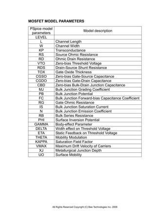
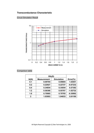
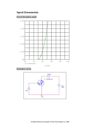
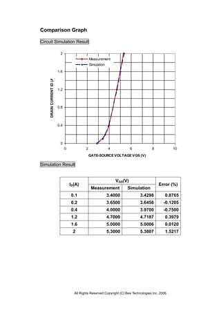
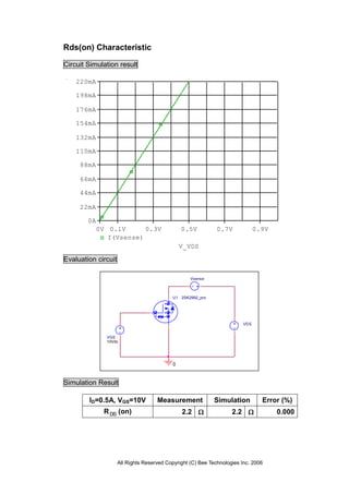
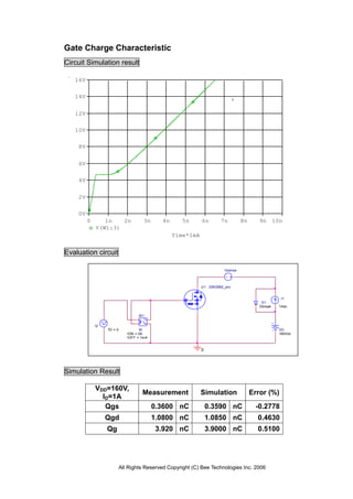
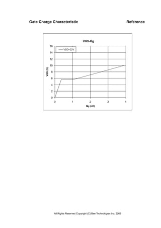
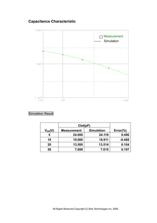
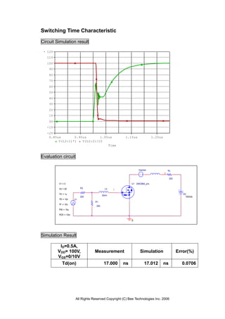
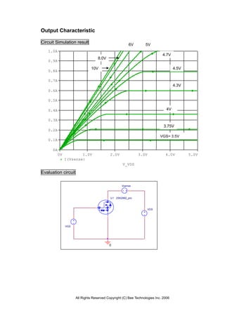
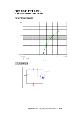
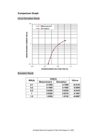
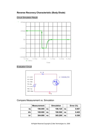
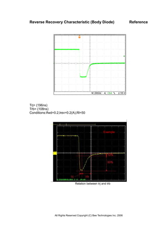
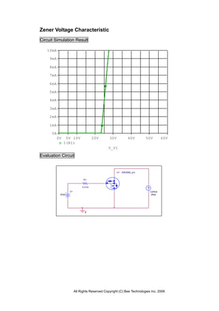

The document reports on the characterization and simulation of a MOSFET (2SK2992) produced by Toshiba, detailing various model parameters, including transconductance and threshold voltage. It presents simulation results for multiple electrical characteristics, such as transconductance, gate charge, capacitance, and switching time, comparing measured values to simulated data. Additionally, the report covers body diode characteristics and includes detailed circuit simulation results and error analysis.


