Download to read offline

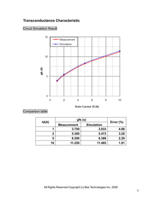
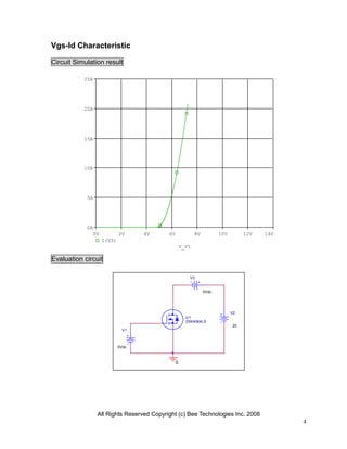
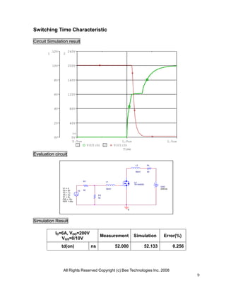
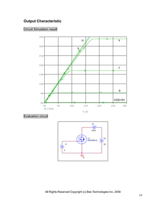
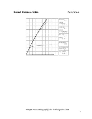
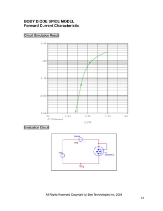

The document presents a detailed device modeling report for a MOSFET (2SK4064LS) manufactured by Sanyo, incorporating various electrical parameters and characteristics. It includes simulation results comparing measurement and modeling data for transconductance, gate charge, capacitance, switching time, and output characteristics alongside associated errors. The report emphasizes the accuracy of the simulations across different operational conditions and characteristics.


![Getting Started with Apache Spark: Big Data Made Simple [Free Meetup]](https://cdn.slidesharecdn.com/ss_thumbnails/apachesparkgettingstarted-260203175547-8361bcc3-thumbnail.jpg?width=640&height=640&fit=bounds)

