Download to read offline


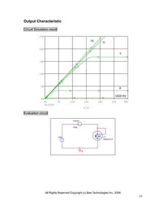
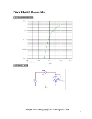
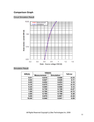
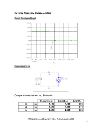

This document summarizes the modeling and simulation of a MOSFET transistor. It includes: 1) Details of the MOSFET component being modeled, including part number, manufacturer, and model parameters. 2) Results of simulations characterizing key electrical properties of the MOSFET, such as transconductance, capacitance, switching time, and forward/reverse current. 3) Comparisons of measurement data and simulation results showing good agreement between the measured and modeled behavior.


