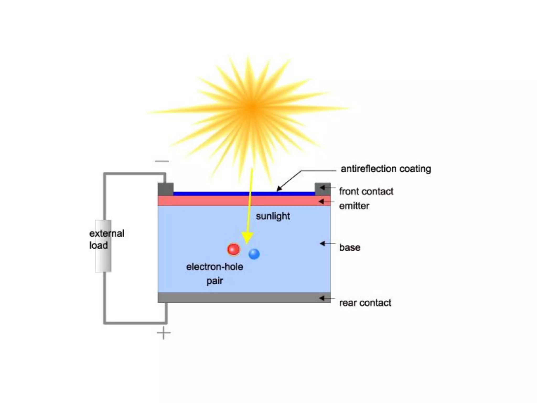
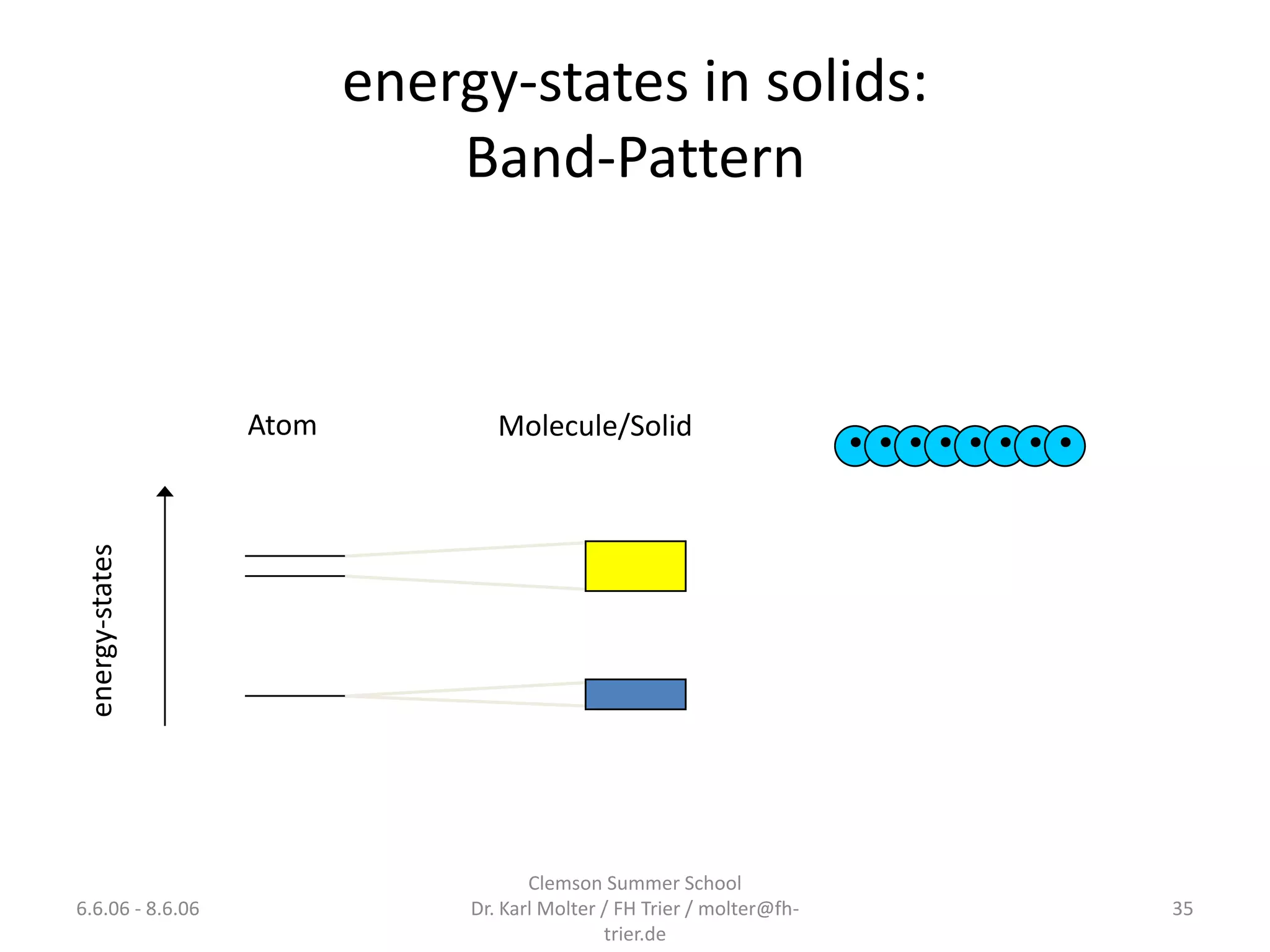
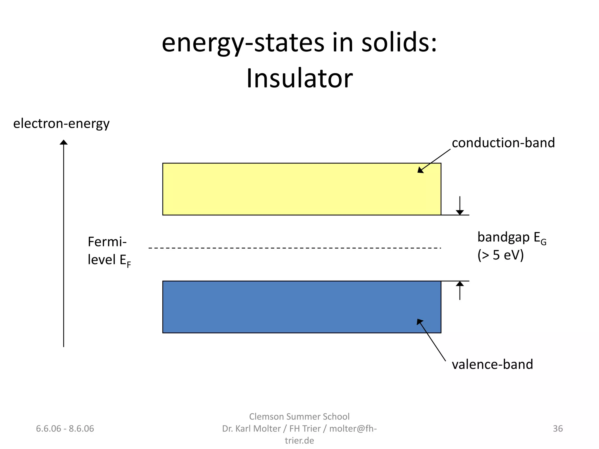
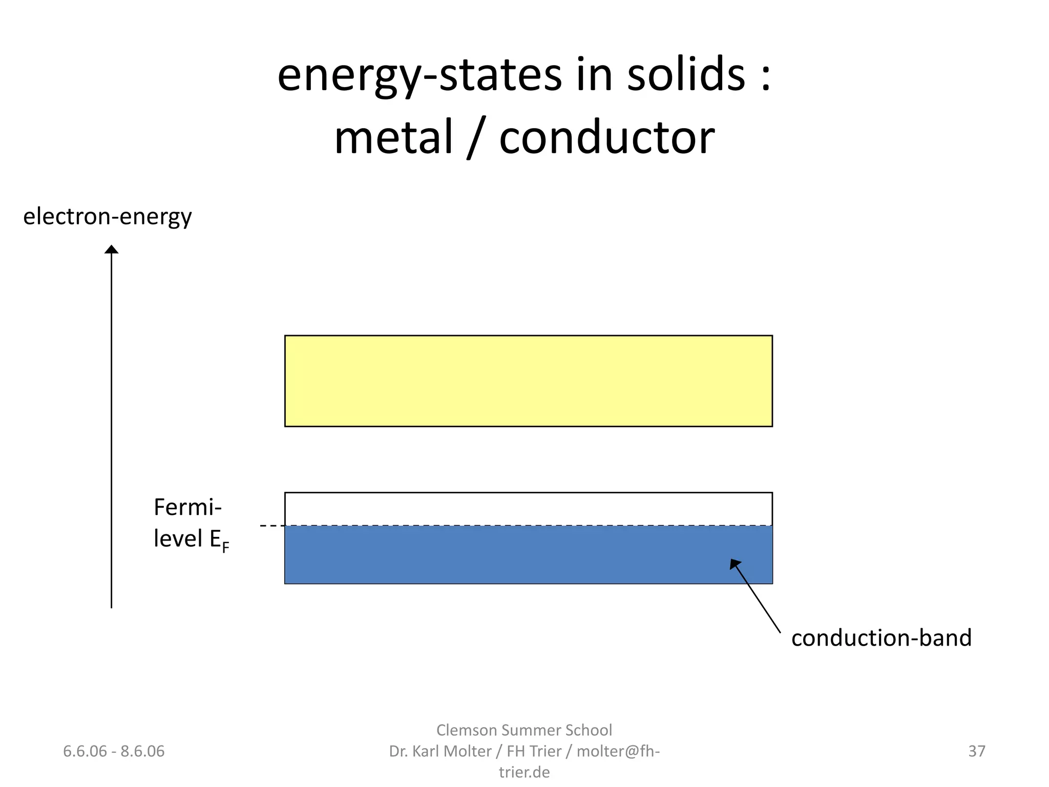
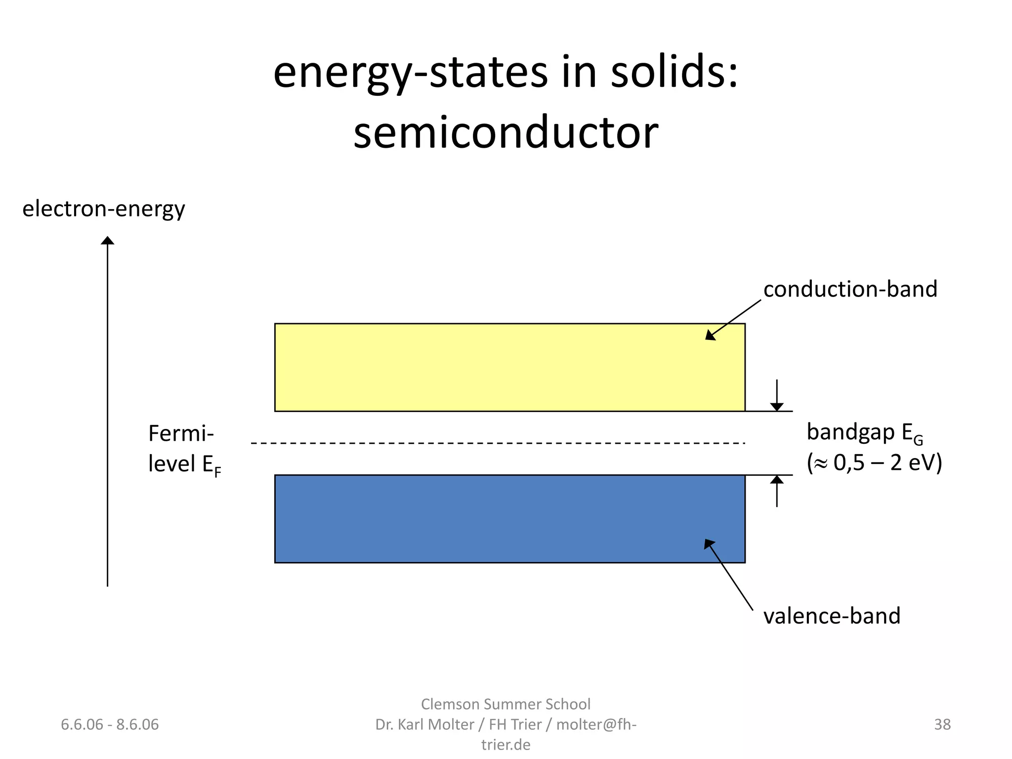
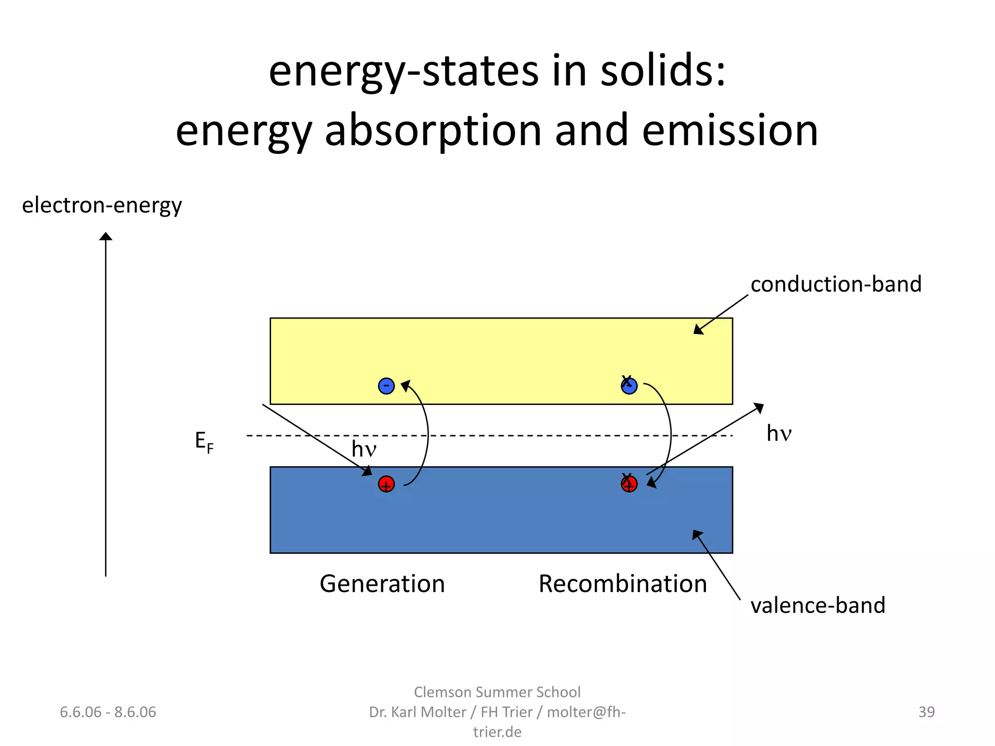
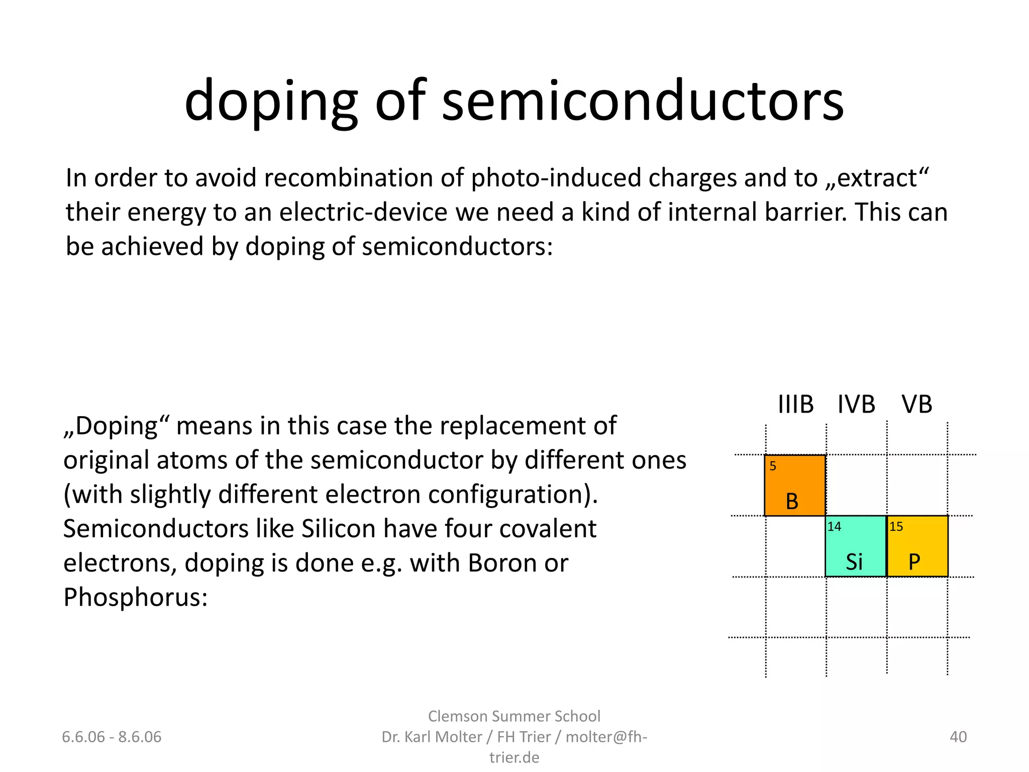
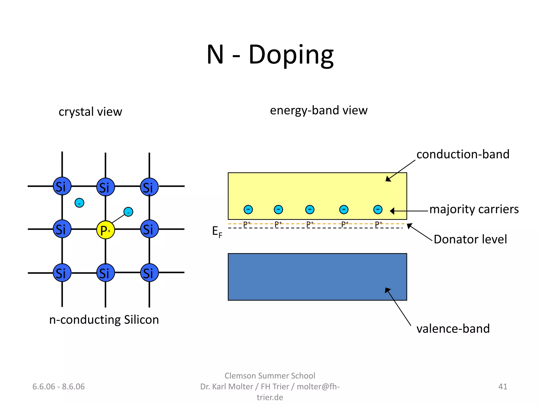
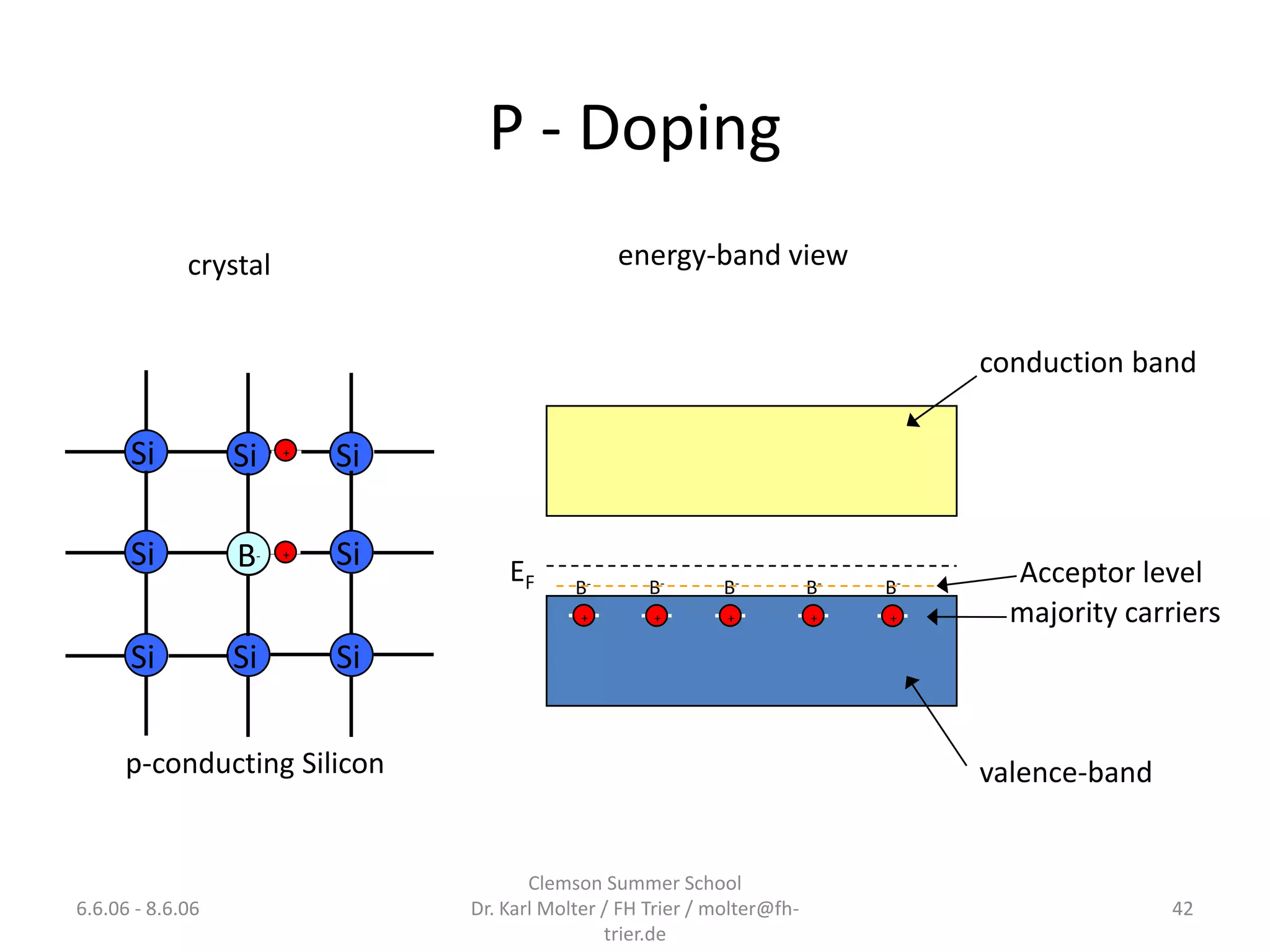
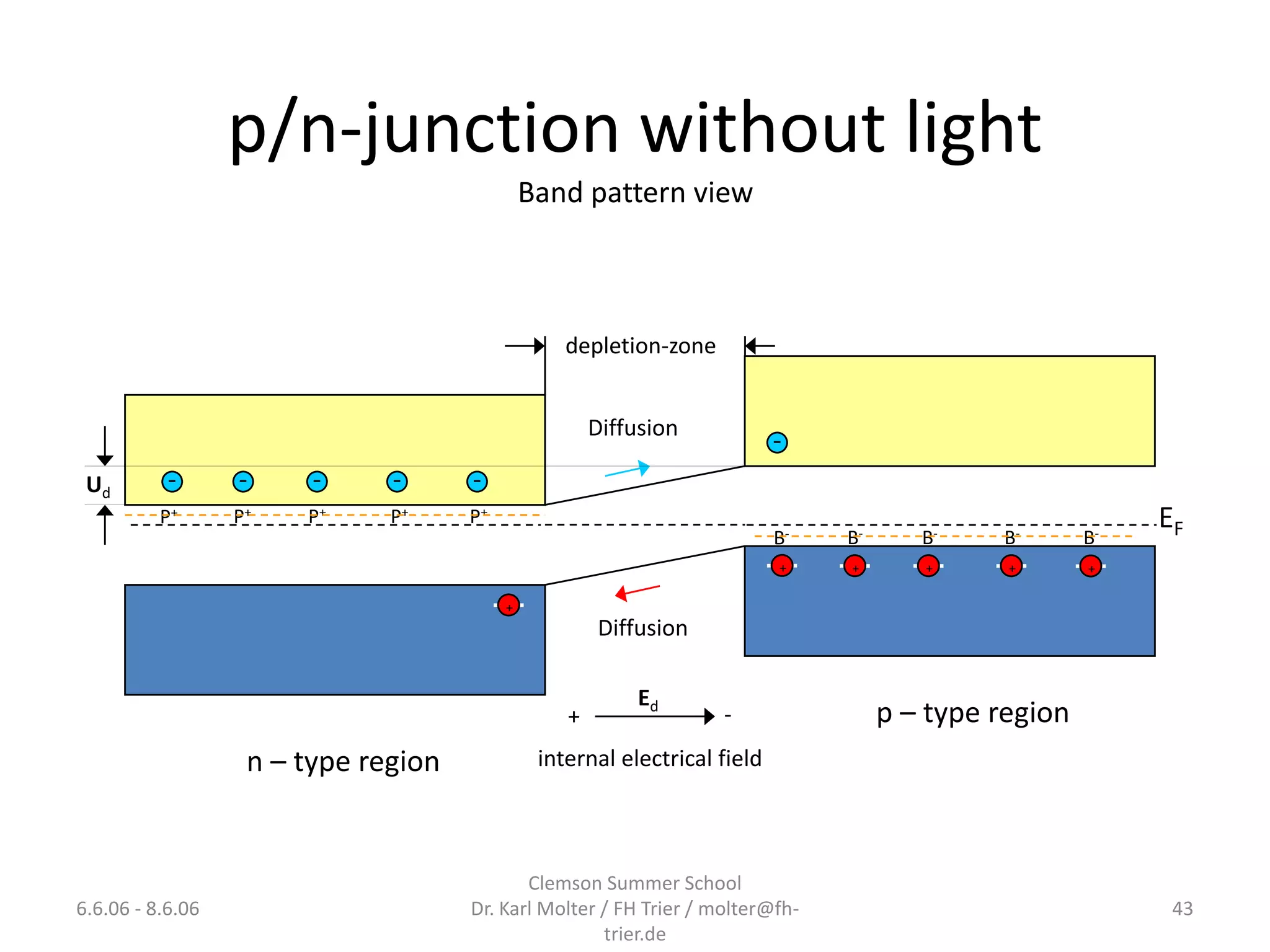
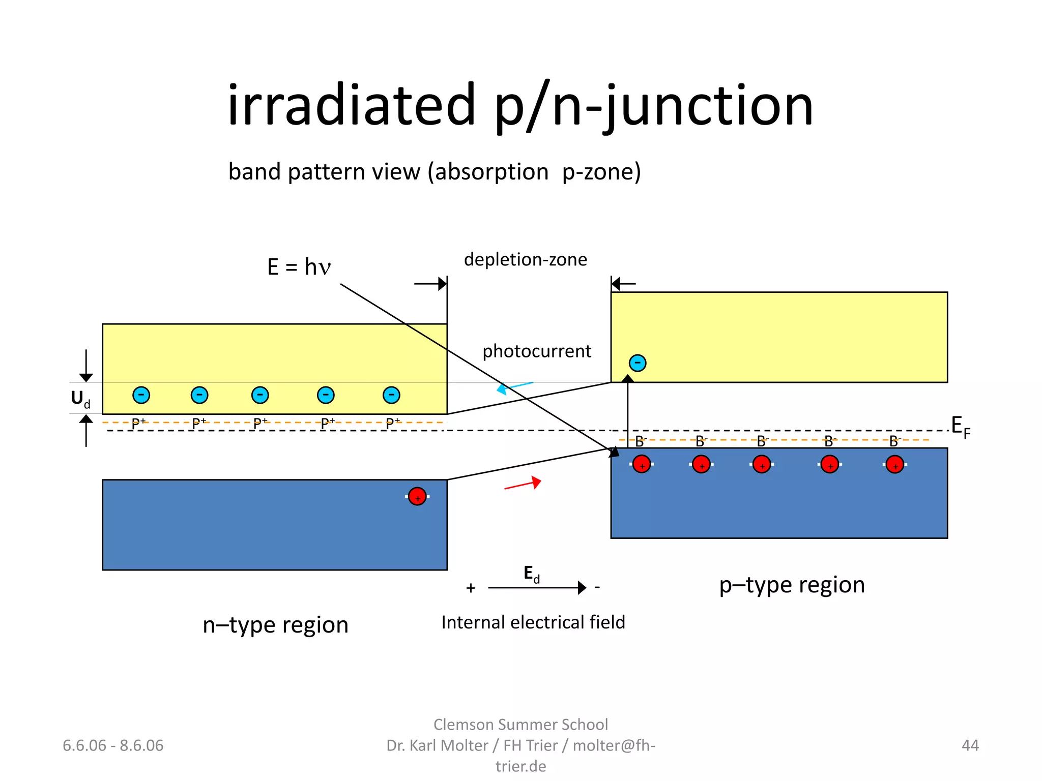
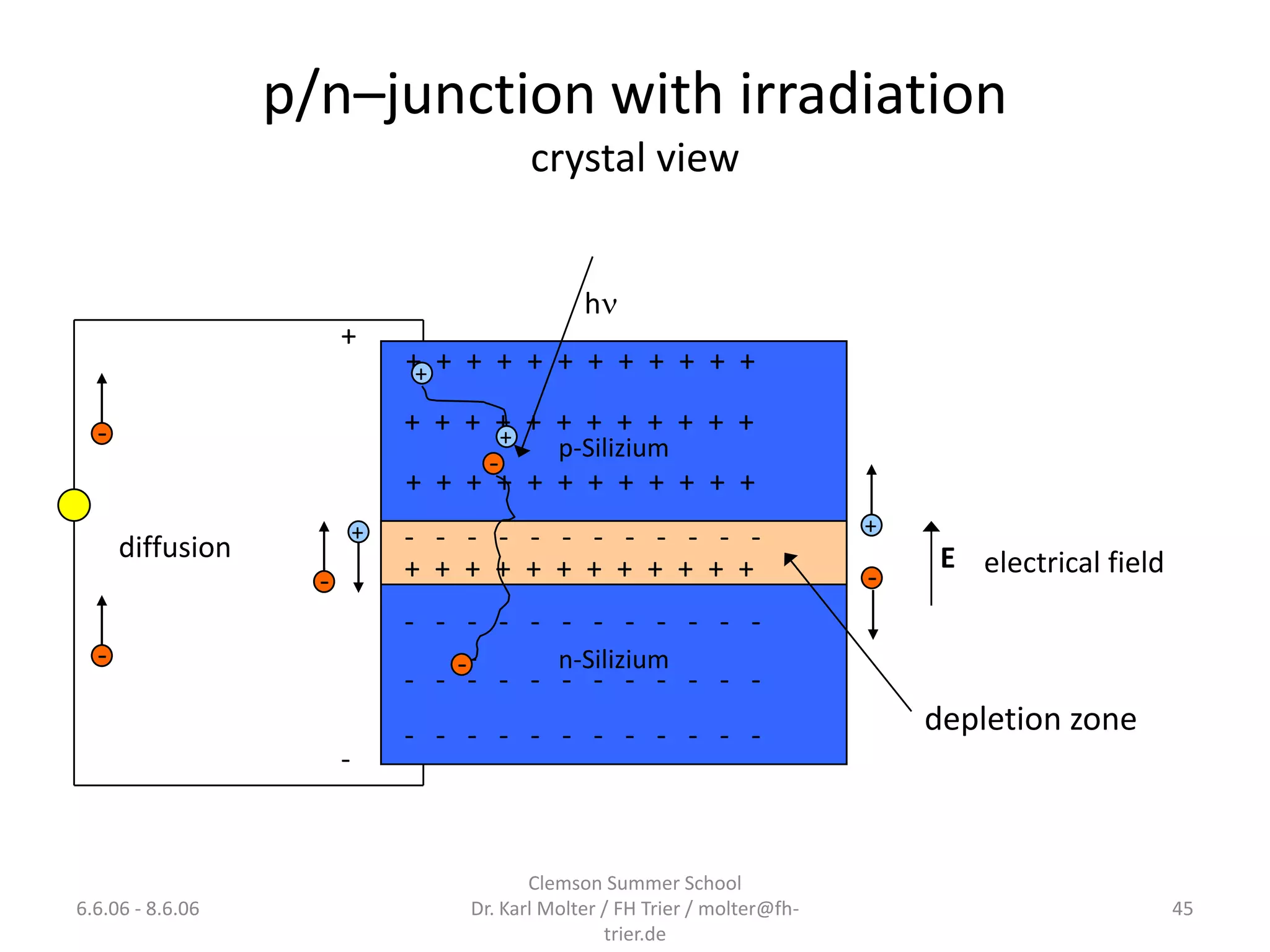
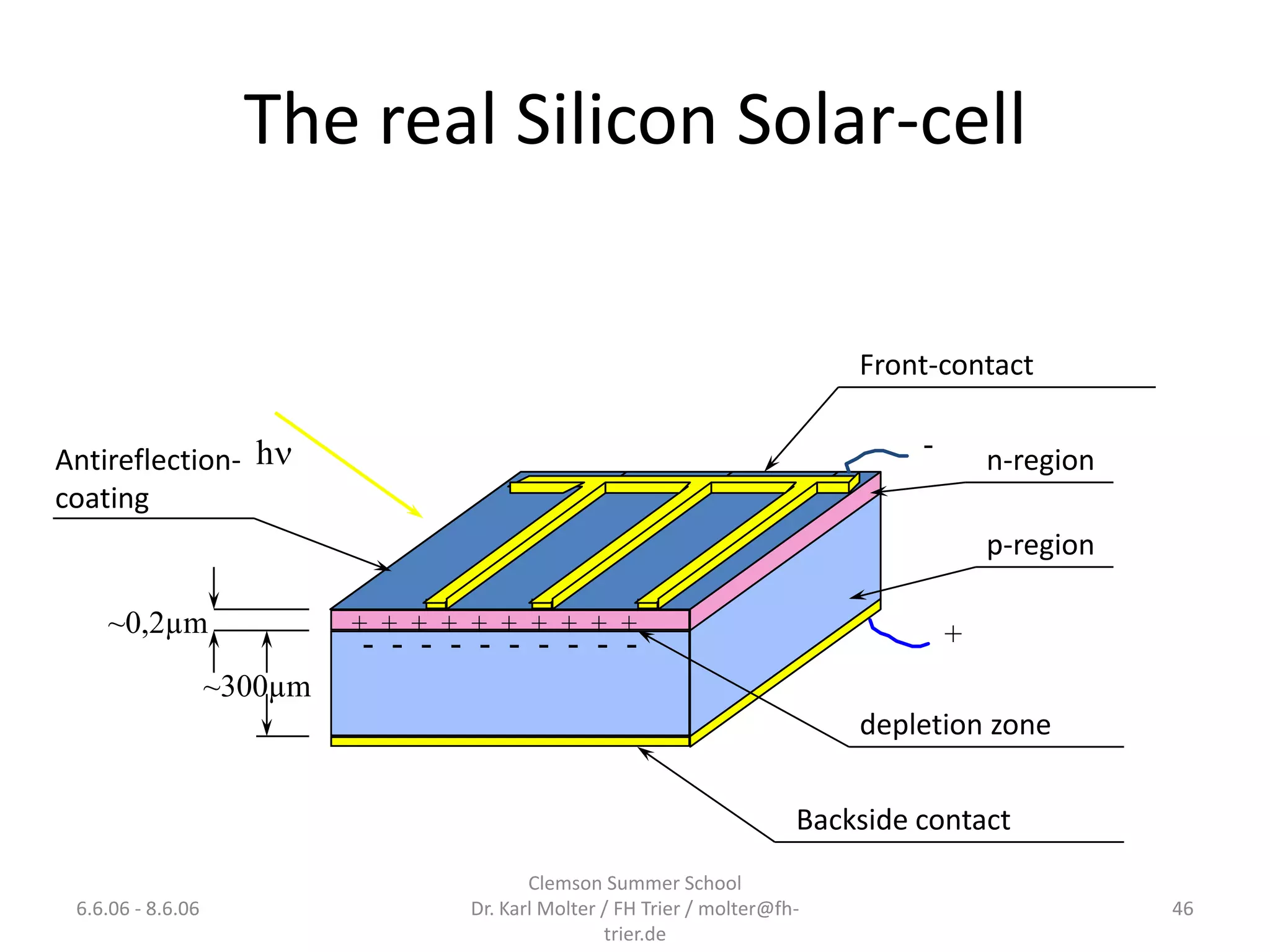
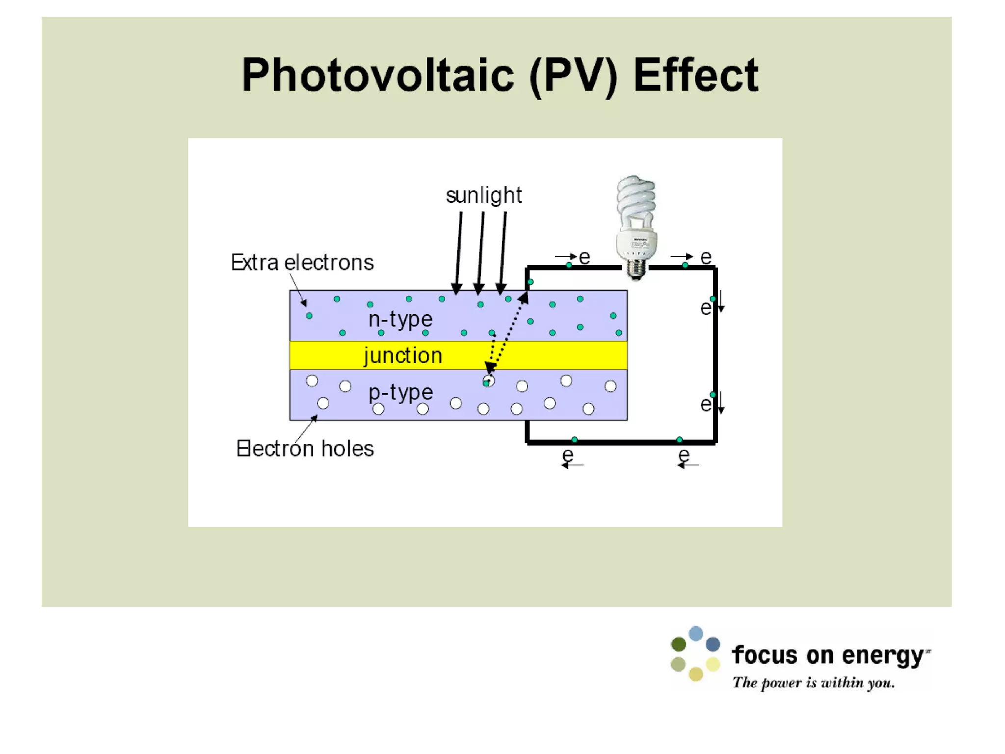
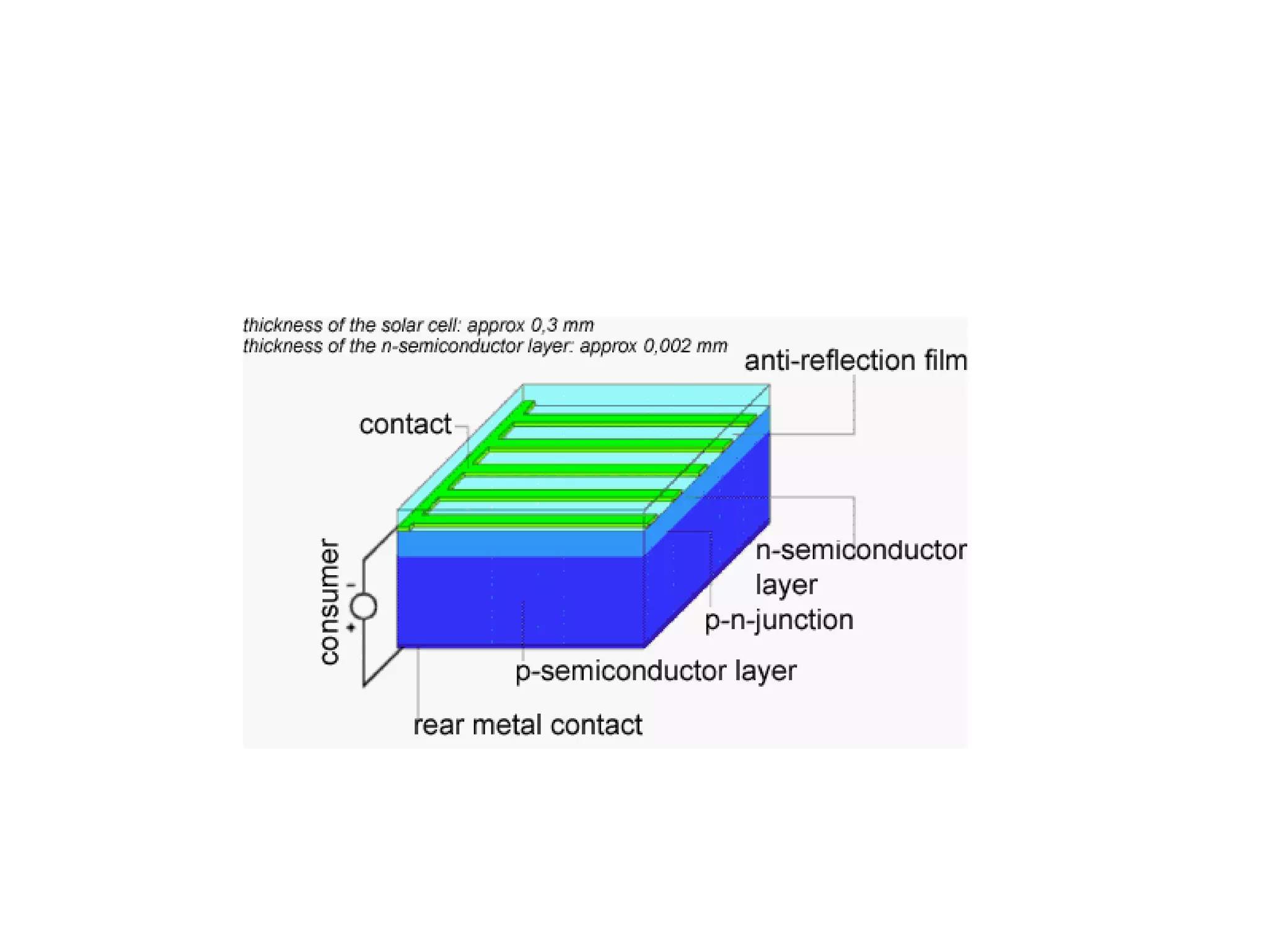
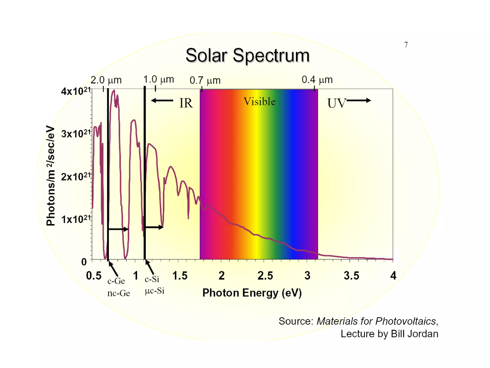
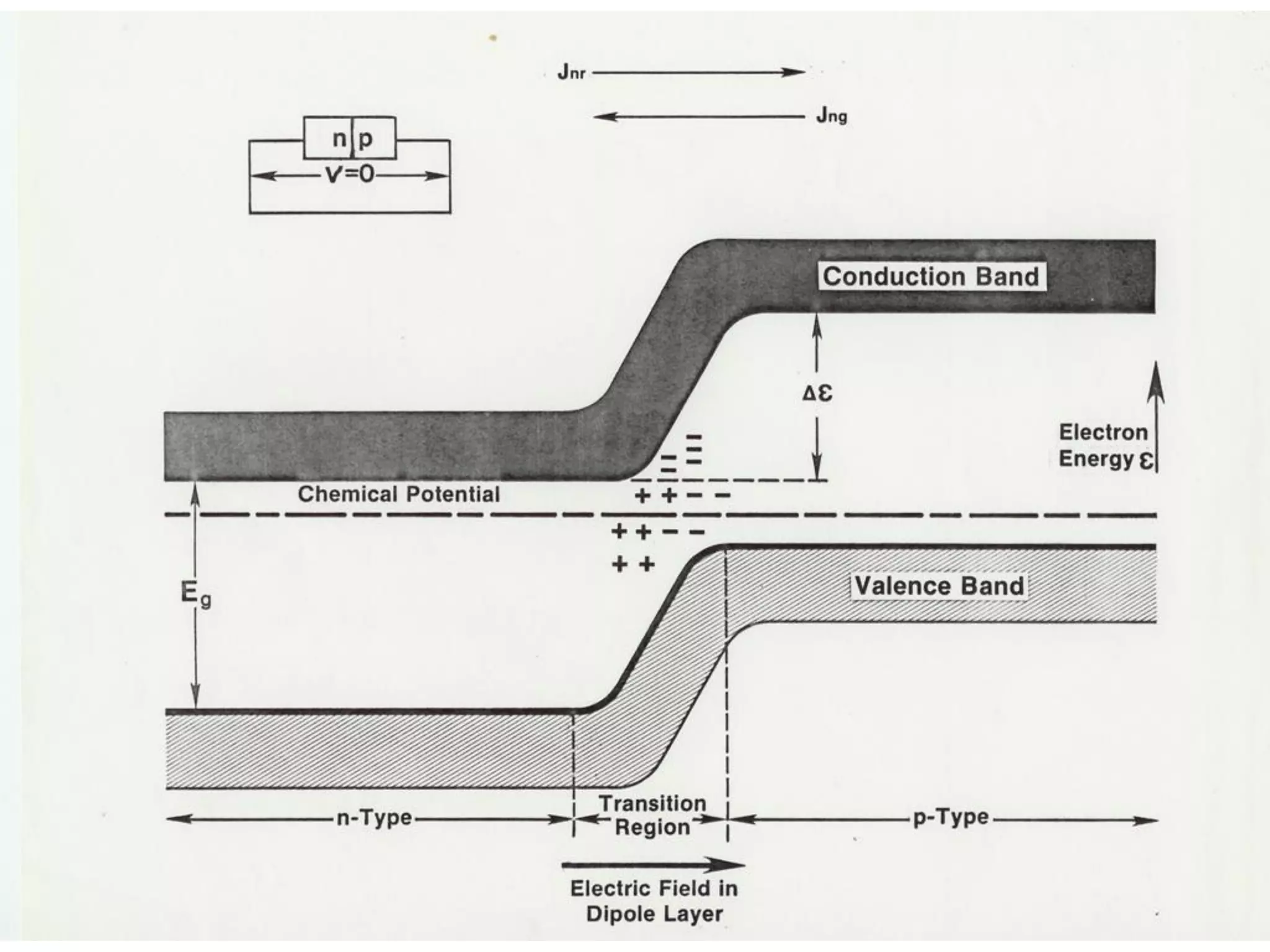
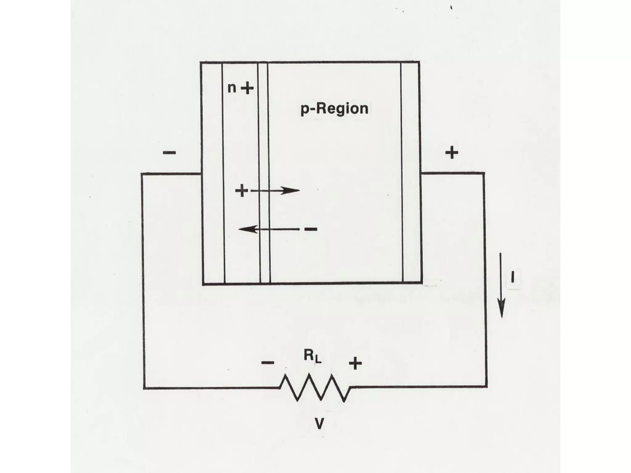
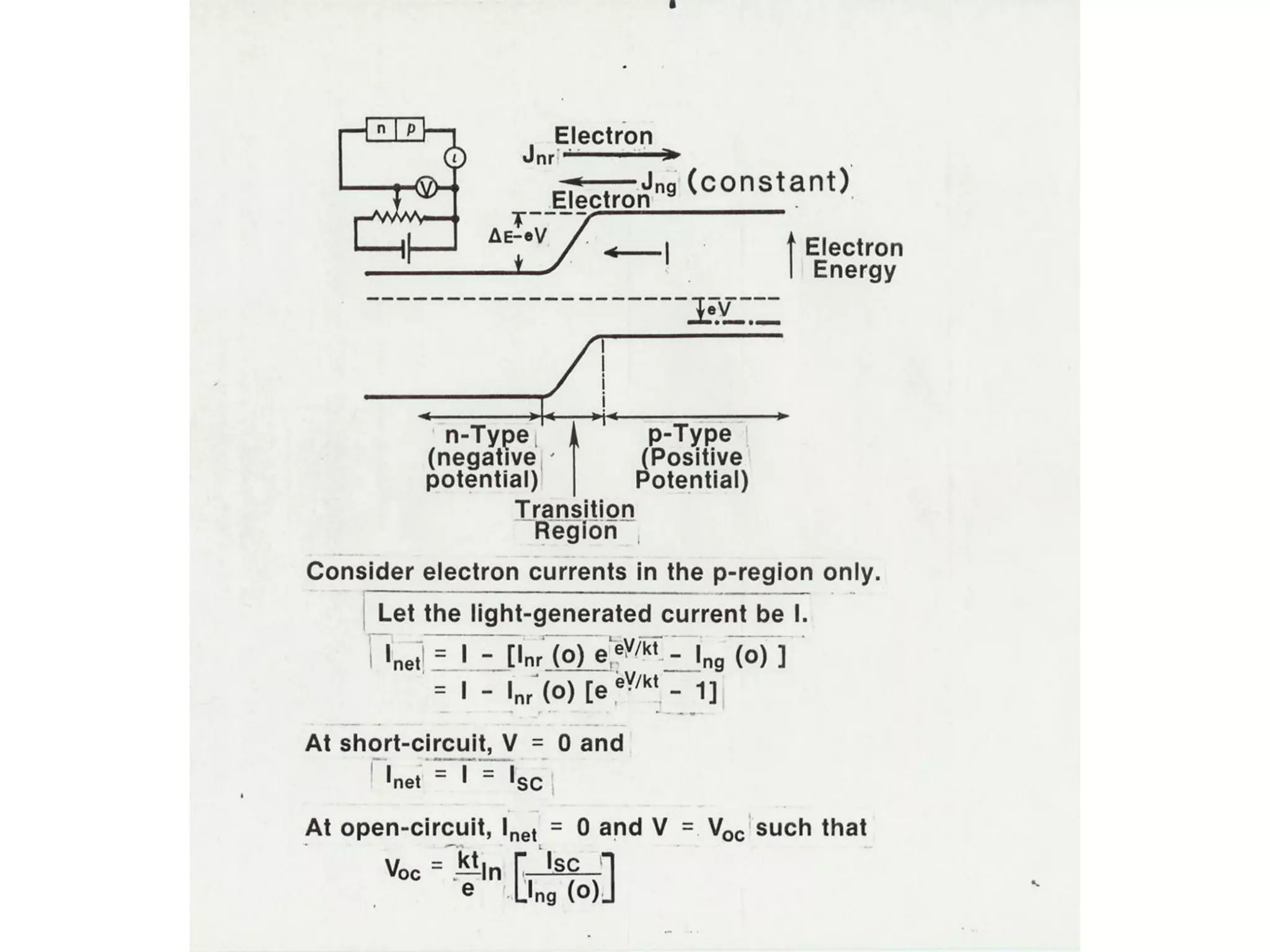
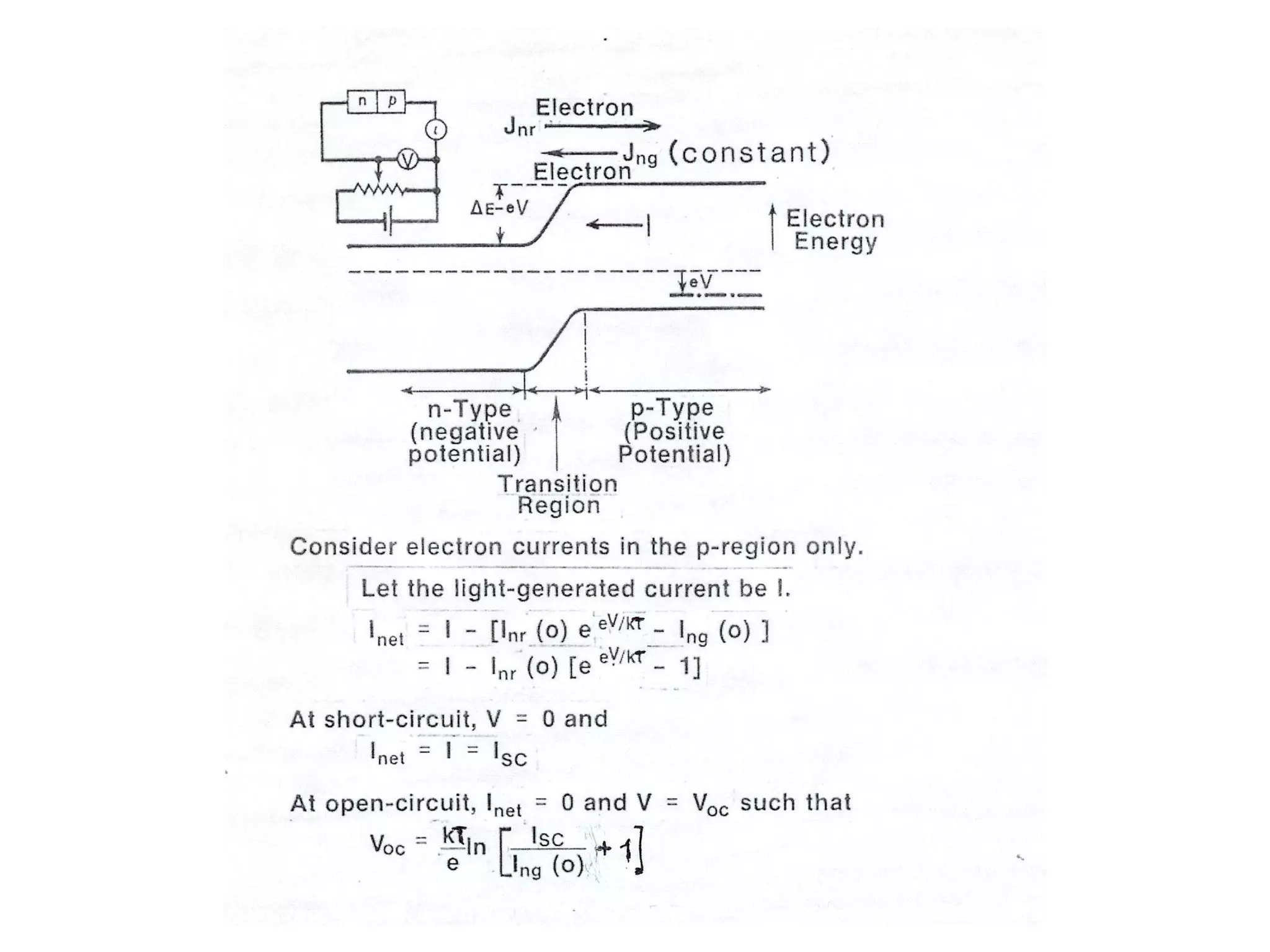
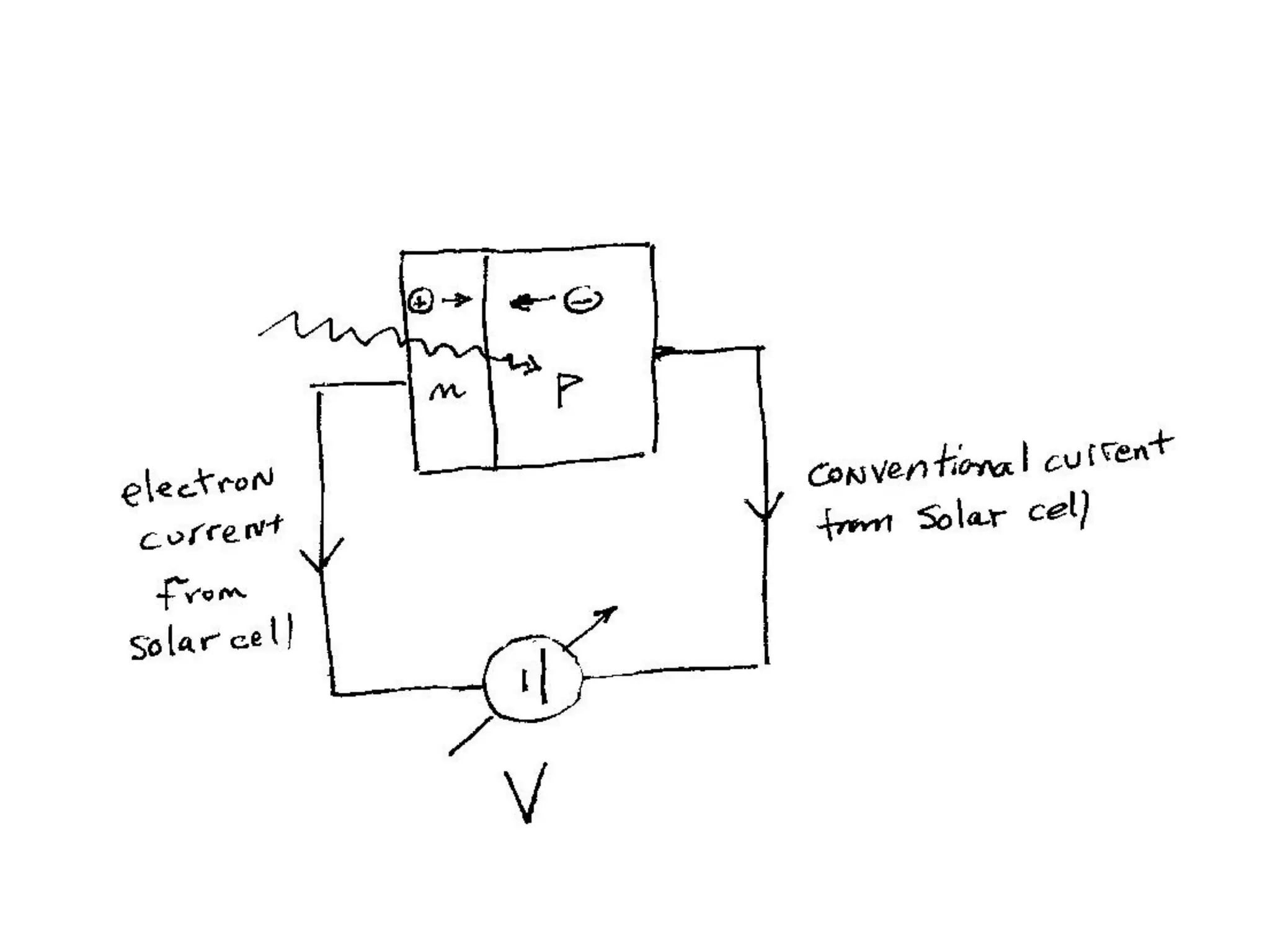
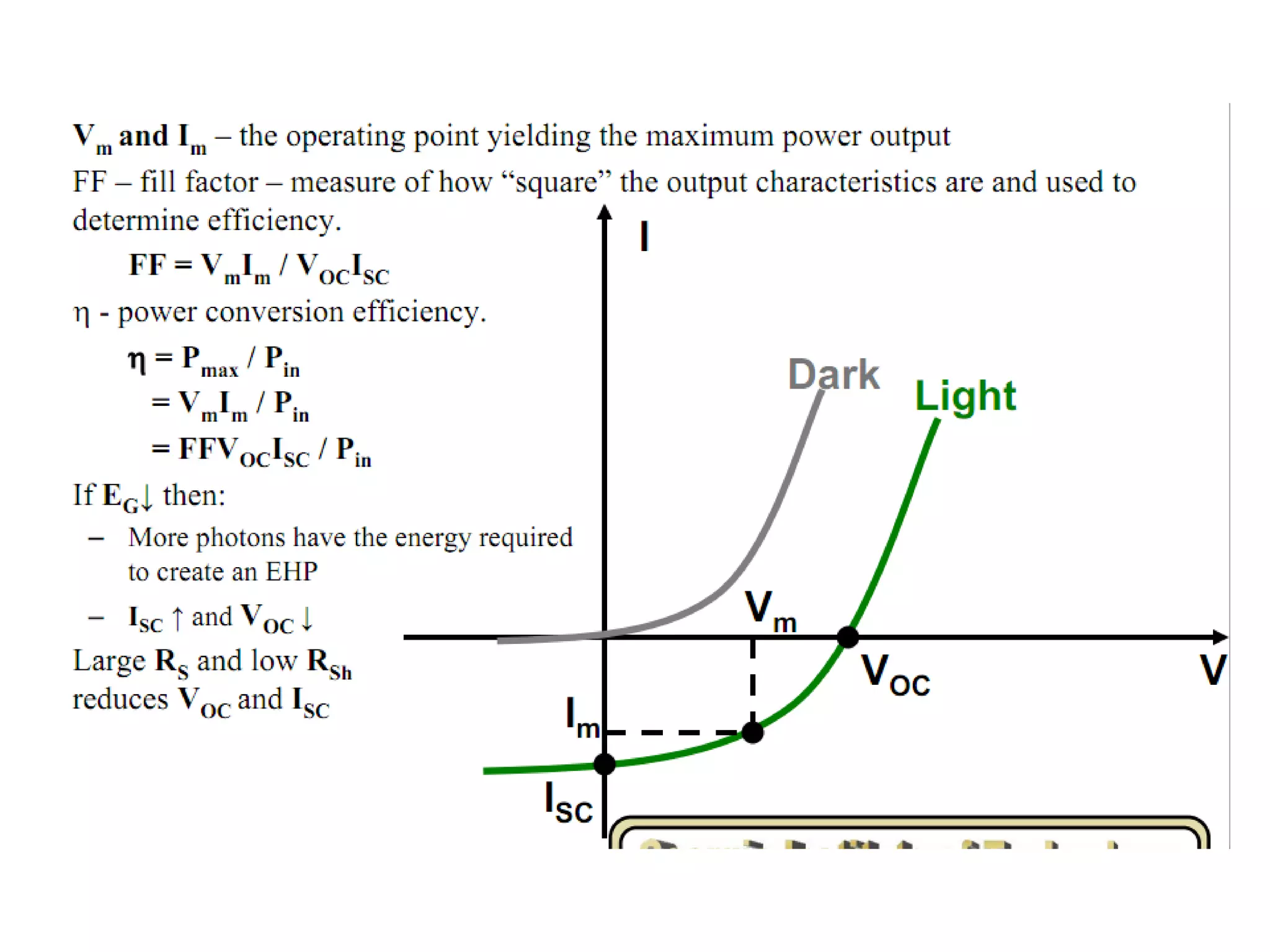
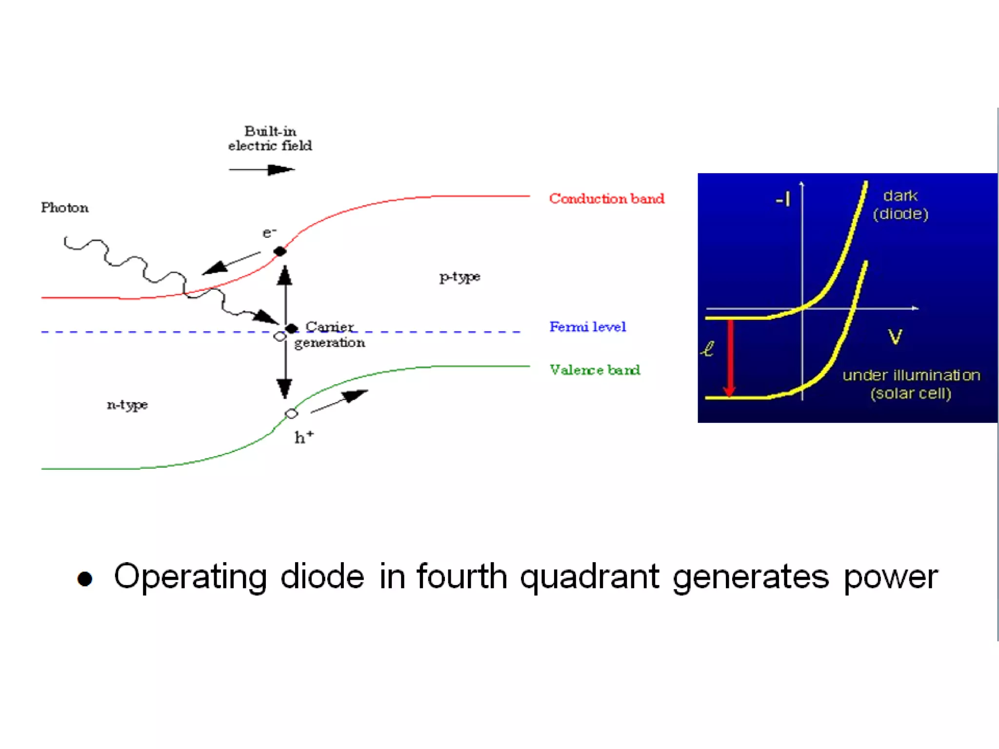
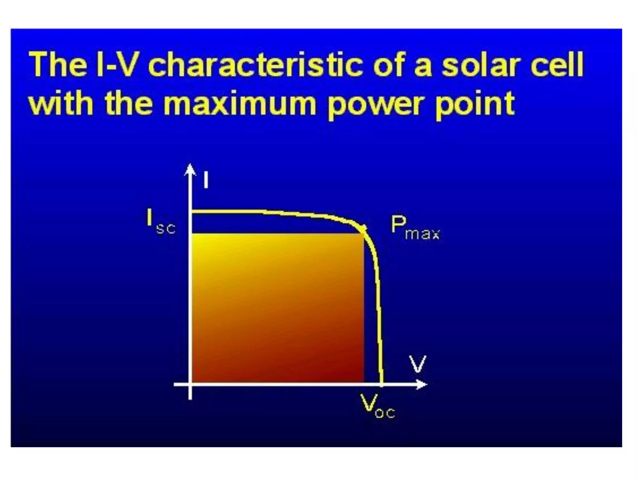
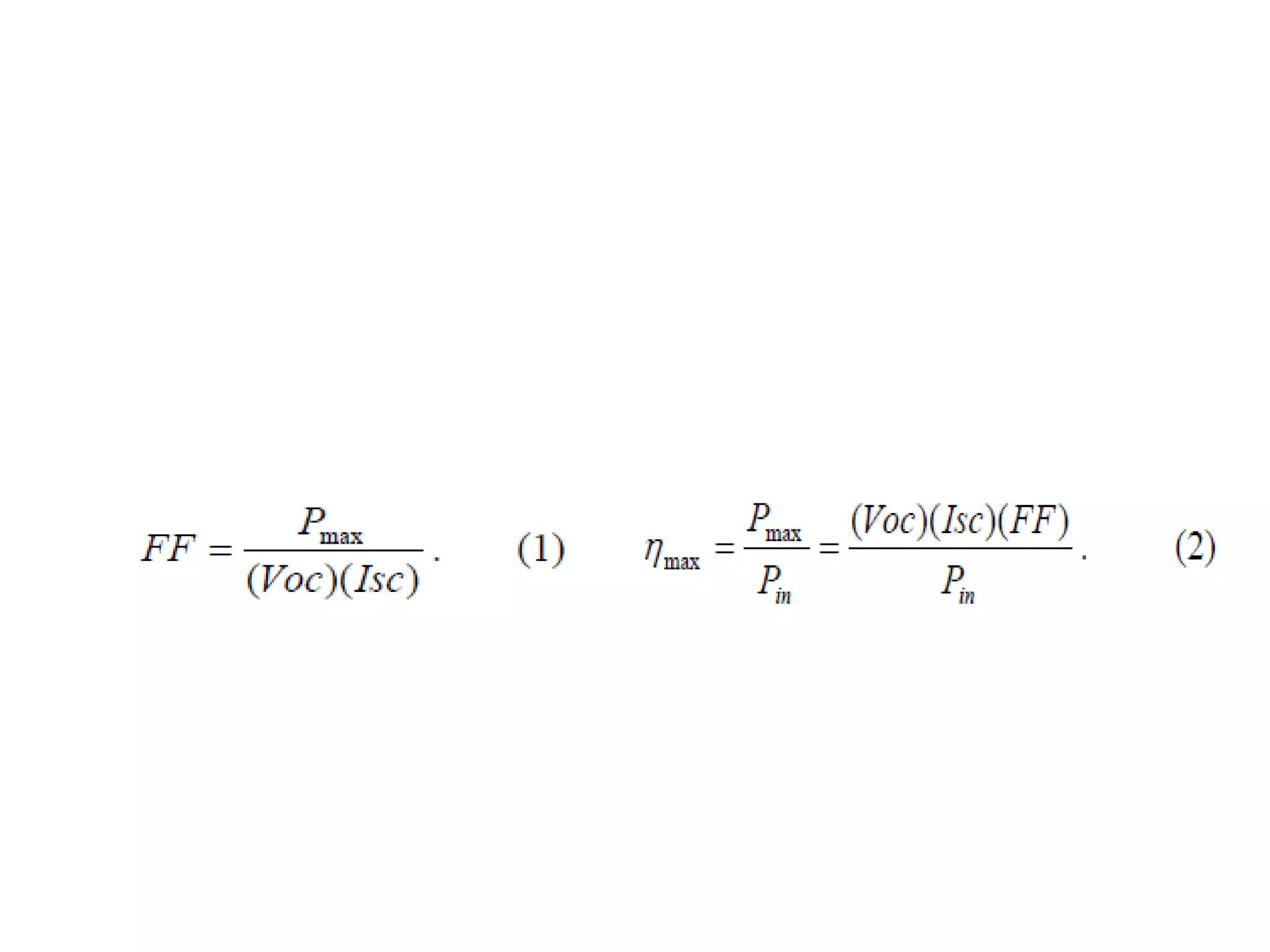
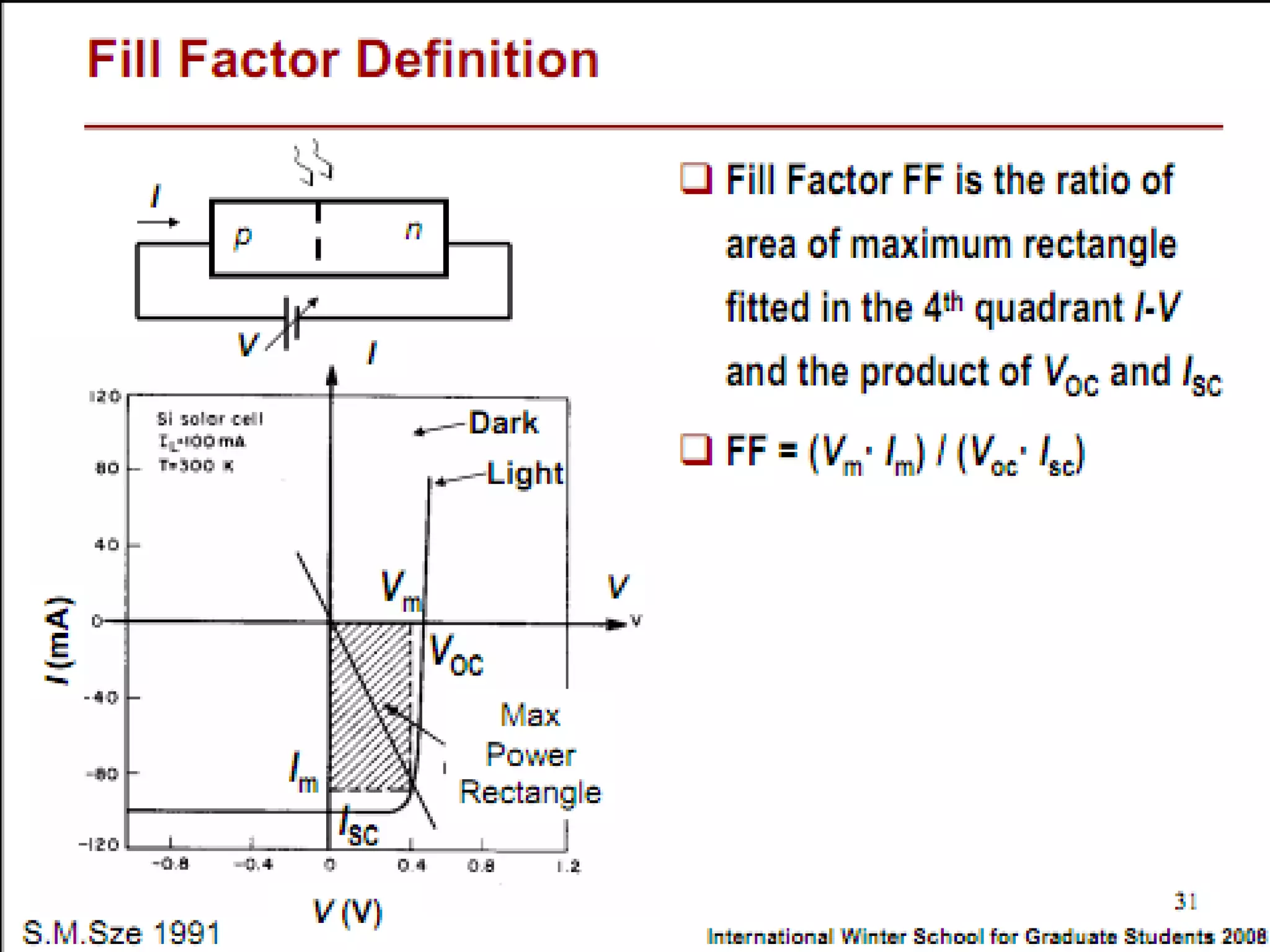
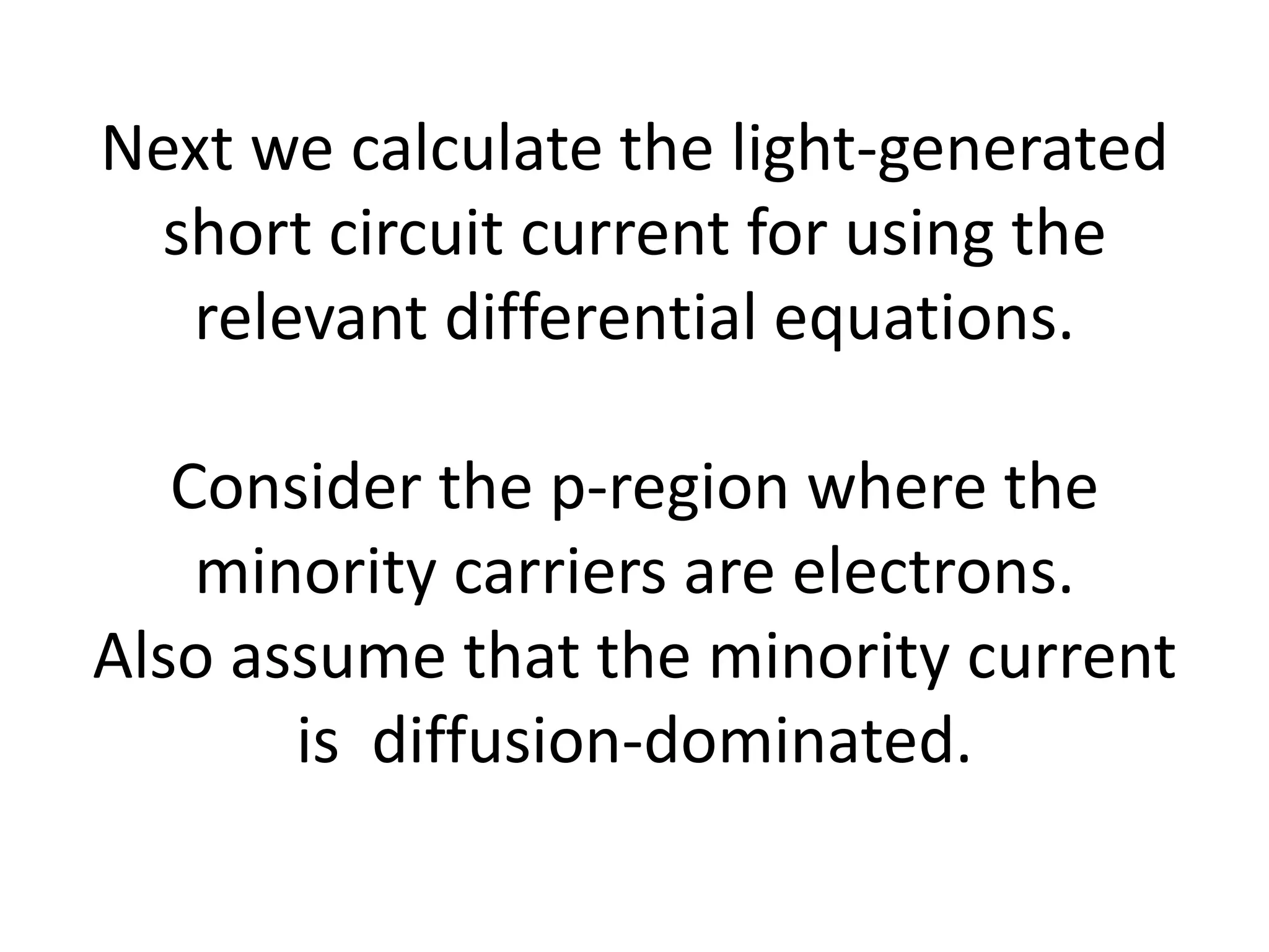
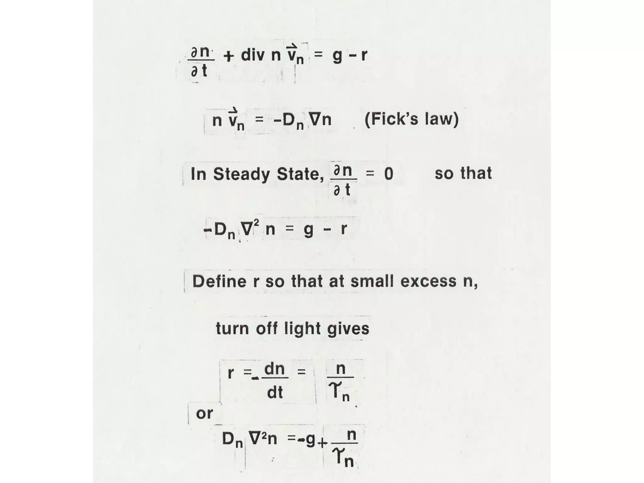
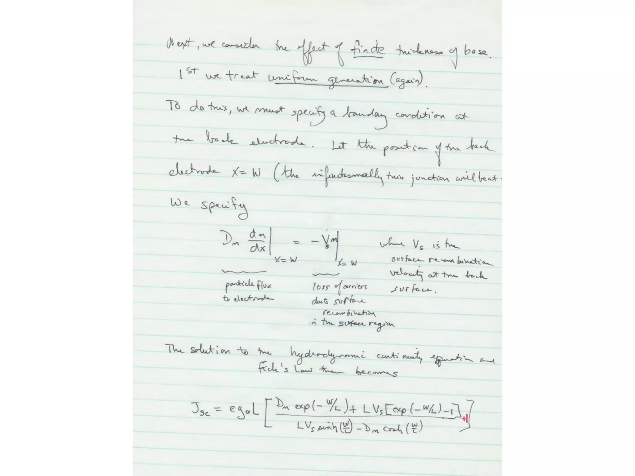
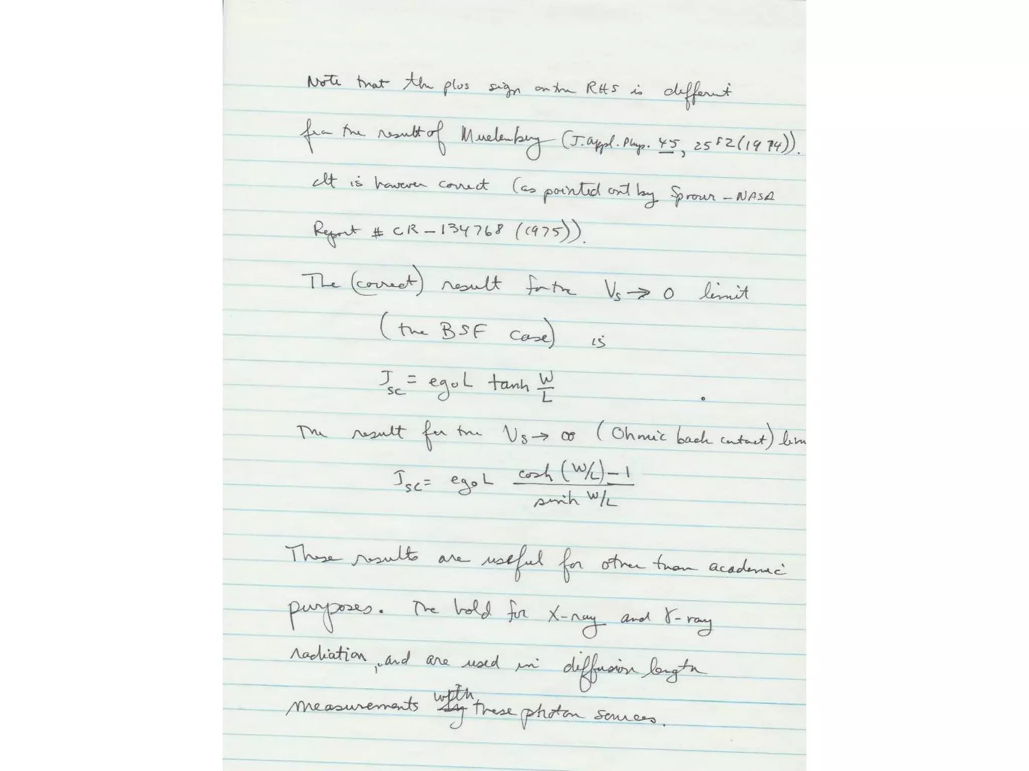
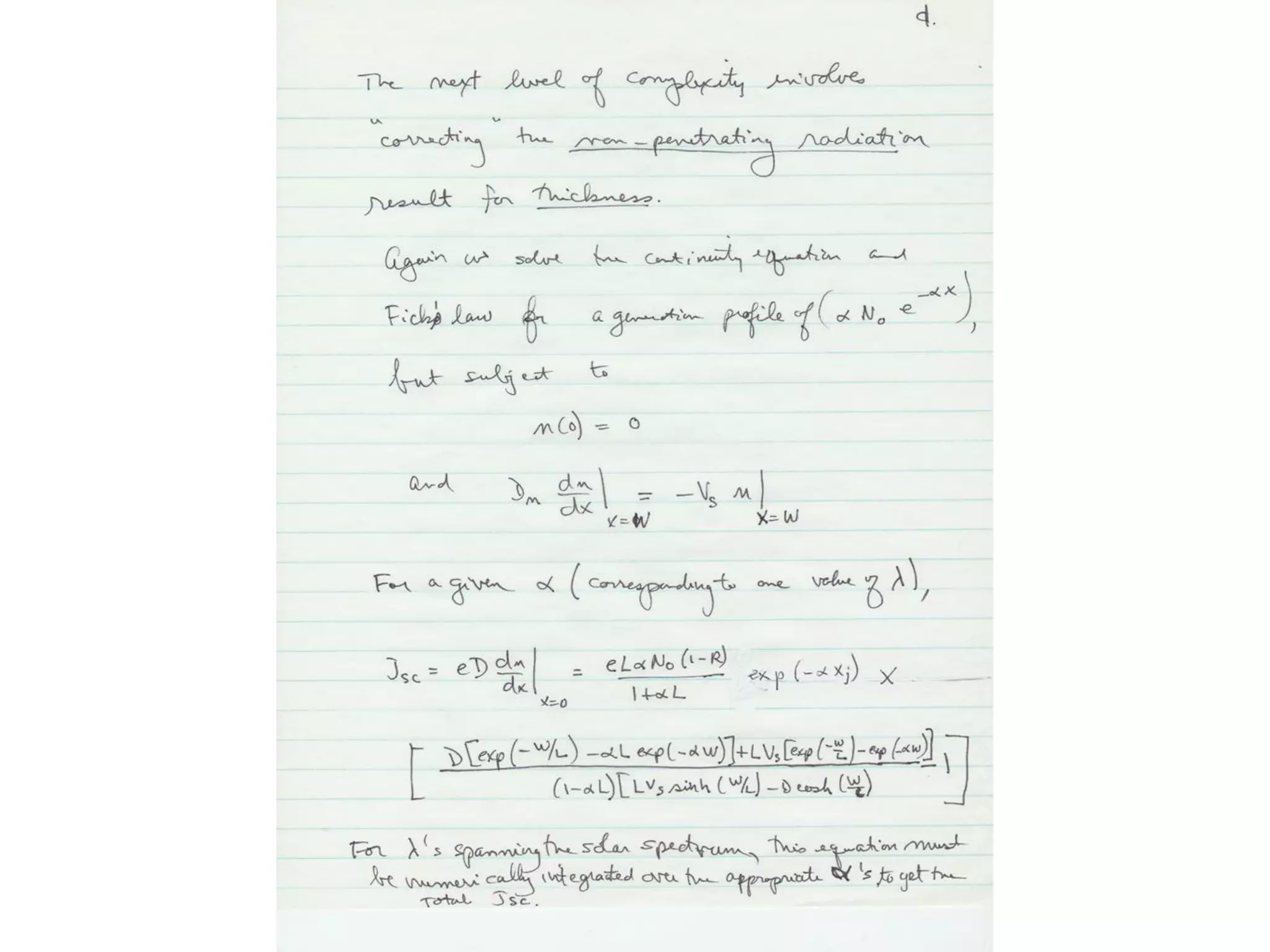
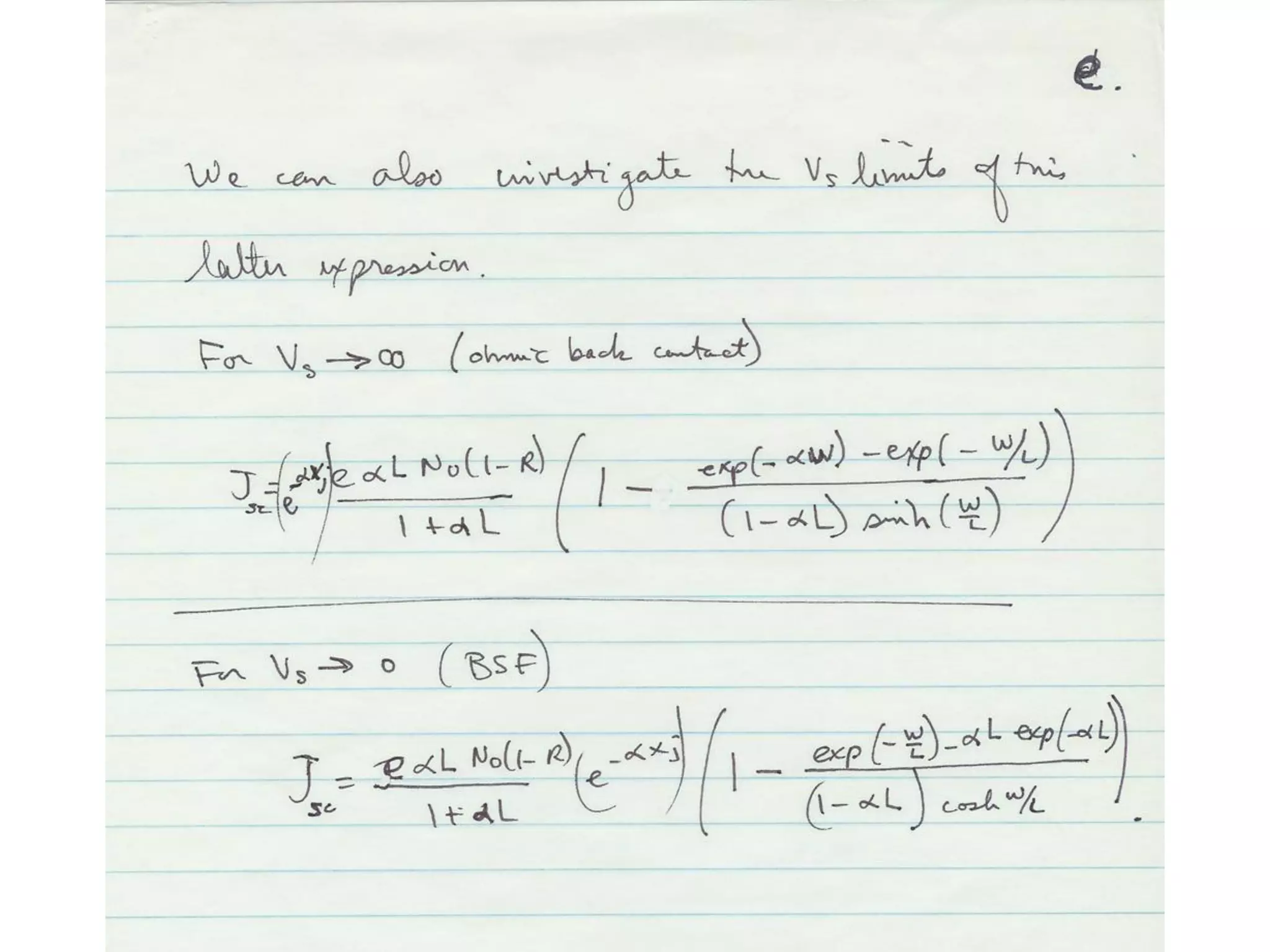
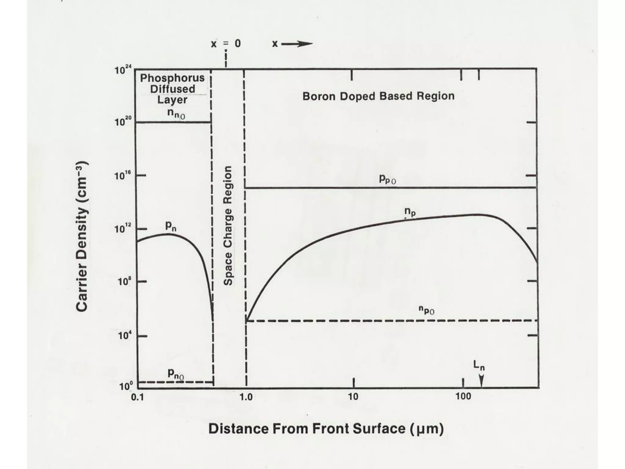
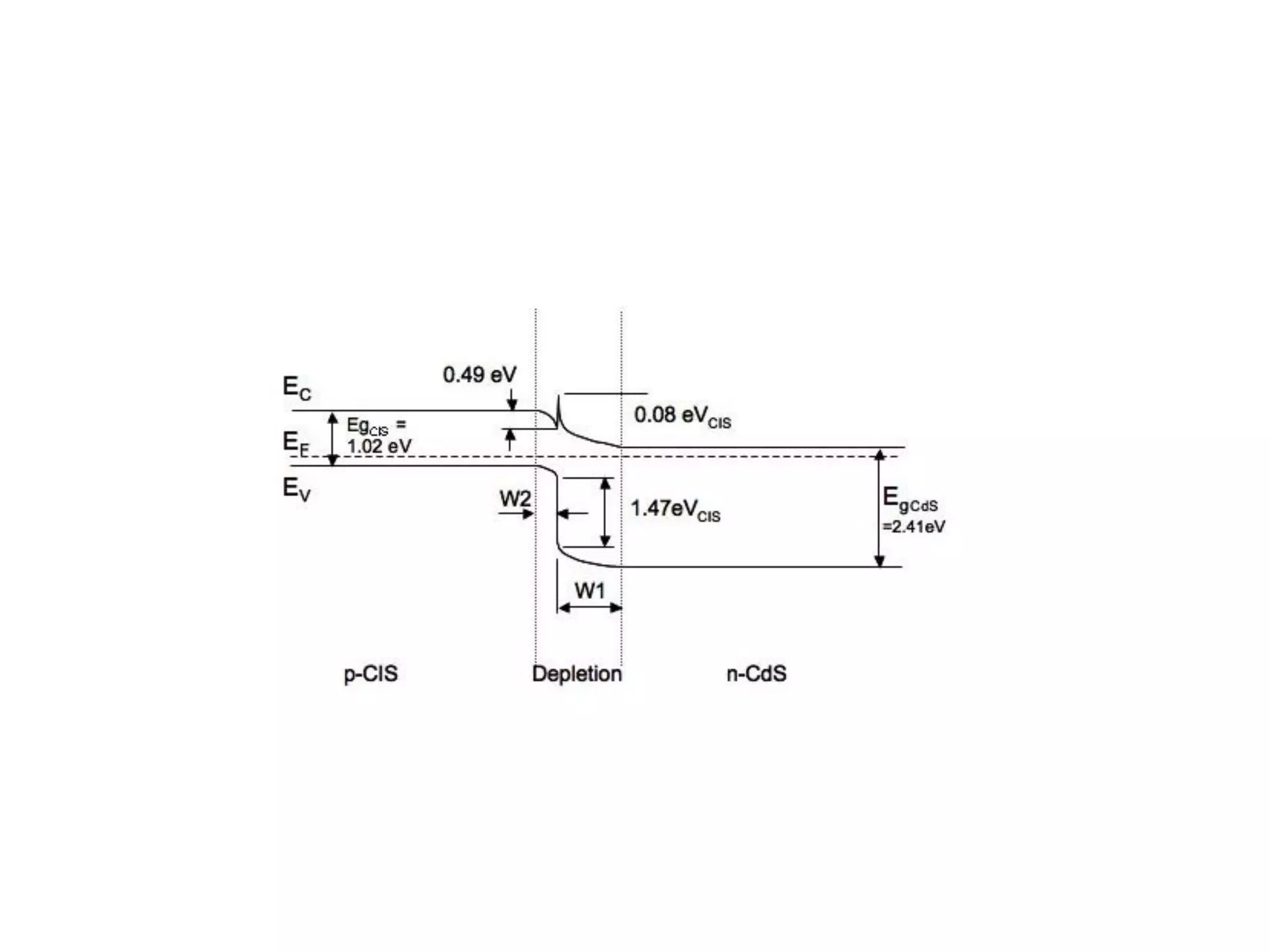
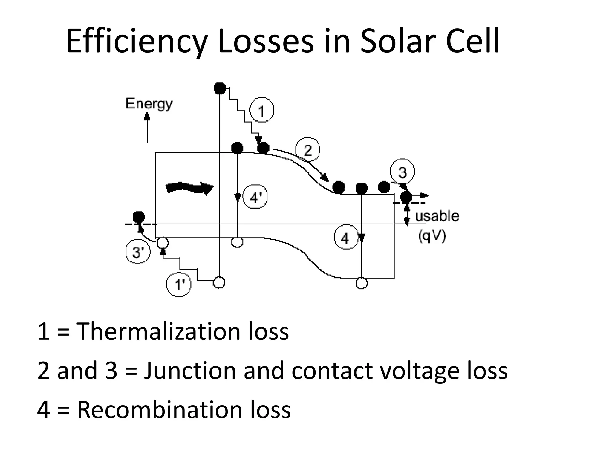
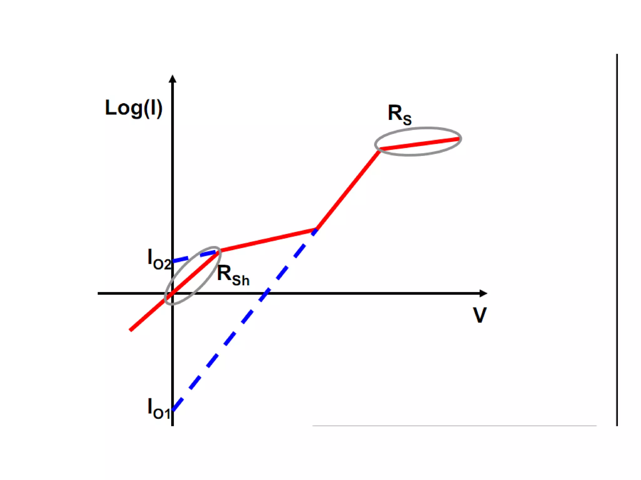
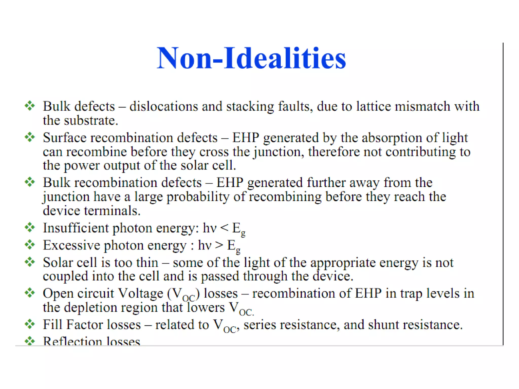
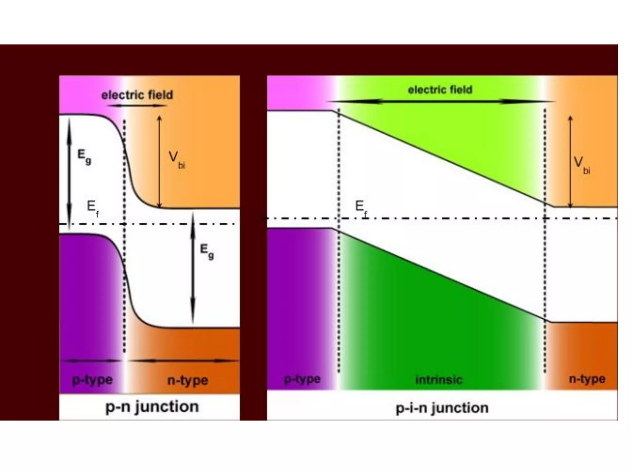
Lecture 4
Solar Cells: Theory I
Lecture 4. Solar cells: Motivation (examples) and Theory
        pn junctions under illumination
        Homojunctions
        Open-circuit voltage, short-
        circuit current
        IV curve, fill factor, solar-to-
        electric conversion efficiency
        Carrier generation and
        recombination
         Defects and minority carrier
         diffusion
         Current due to minority carrier
         diffusion:
         Solution to the diffusion
         differential equation under
         Spatially-homogeneous
         generation, and
         under Inhomogeneous
         generation
         Effect of an electric field
         Heterojunctions
Celdas Solares
LA TECNOLOGIA FOTOVOLTAICA ESTA
CONTEMPLADA PARA       APLICACIÓN
AUTONAMA. ELECTRIFICACION RURAL,
BOMBEO DE AGUA, ILUMINACION DE
CARRATERAS, MONITOREO DE NIVELS DE
AGUA EN RIOS ETC. SON ALGUNOS
EJEMPLOS
ESTA TECNOLOGIA CONVIERTE LA
ENERGIA SOLAR DIRECTO A ENERGIA
ELECTRICA DC UTILIZABDO MODULOS
FOTOVOLTAICOS (CELDAS SOLARES)
EL MATERIAL DE CONSTRUCCION DE
CELDA SOLAR SE LLAMA
“SEMICONDUCTOR”
Example: PV-Roof and Front,


                                 Clemson Summer School
6.6.06 - 8.6.06           Dr. Karl Molter / FH Trier / molter@fh-   16
                                          trier.de
Alwitra Solar-foil


                            Clemson Summer School
6.6.06 - 8.6.06      Dr. Karl Molter / FH Trier / molter@fh-   17
                                     trier.de
Example: Sports-Center Tübingen


                           Clemson Summer School
6.6.06 - 8.6.06     Dr. Karl Molter / FH Trier / molter@fh-   18
                                    trier.de
Example:
             Fire-brigade


                                Clemson Summer School
6.6.06 - 8.6.06          Dr. Karl Molter / FH Trier / molter@fh-   19
                                         trier.de
Example: BP Showcase


                              Clemson Summer School
6.6.06 - 8.6.06        Dr. Karl Molter / FH Trier / molter@fh-   20
                                       trier.de
Crystalline Silicon

• Polycrystalline Si
   – Made from melting Si into ingots, slicing off
     wafers
   – Cell efficiencies of 14% - 15%
   – Widest use
• Monocrystalline Si
   – “Grown” crystals, more uniform structure
   – Higher cell efficiencies (17% - 22%)
   – Higher cost and better space utilization
• Most often manufactured in framed modules
Amorphous Thin-Film Si


            • Si solution layered onto various
              substrates
            • Conversion efficiencies of 9% to
              12%
            • Some framed module products,
              others bonded to flexible roofing
              materials
            • Very uniform appearance, but less
              effective space utilization
            • Less costly to produce than
              crystalline modules
Building Integrated PV
• Roof tile replacements
• Solar glass
• Thin film bonded to single-ply membrane
  roofing material
Solar-roof shingle


                            Clemson Summer School
6.6.06 - 8.6.06      Dr. Karl Molter / FH Trier / molter@fh-   24
                                     trier.de
25 m2
300 m2
Concentrating Solar Panels

• Fresnel lenses in tracking panels concentrate
  light 500:1 on smaller amount of Si (Xerox
  PARC Research)
• Tracking mirrors focus sunlight on stationary Si
  (Energy Innovations “Sunflower”)
Energía Fotovoltaica

                          Efecto Fotovoltaico


                                                       LUZ         SOLAR
El Efecto Fotovoltaico (FV):
 es la generación de un voltaje en
las terminales de un captador
solar cuando éste es iluminado. Si                    CELDA
a las terminales del captador se le                   SOLAR
conecta un aparato eléctrico, por
ejemplo, un foco, entonces el foco
se enciende debido a la corriente                      Voltaje fotogenerado
eléctrica que circula por él. Esta es
la evidencia física del fenómeno
fotovoltaico.
                                        Corriente eléctrica fotogenerada
History

   • 1839: Discovery of the photoelectric effect
     by Bequerel
   • 1873: Discovery of the photoelectric effect
     of Selen (change of electrical resistance)
   • 1954: First Silicon Solar Cell as a result of
     the upcoming semiconductor technology (
     = 5 %)

                          Clemson Summer School
6.6.06 - 8.6.06    Dr. Karl Molter / FH Trier / molter@fh-   33
                                   trier.de
energy-states in solids:
                             Band-Pattern


                  Atom           Molecule/Solid
                                                                        • • • • • • • •
 energy-states


                                     Clemson Summer School
6.6.06 - 8.6.06               Dr. Karl Molter / FH Trier / molter@fh-                     35
                                              trier.de
energy-states in solids:
                                 Insulator
electron-energy
                                                                          conduction-band


                Fermi-                                                       bandgap EG
                level EF                                                     (> 5 eV)


                                                                          valence-band


                                       Clemson Summer School
   6.6.06 - 8.6.06              Dr. Karl Molter / FH Trier / molter@fh-                   36
                                                trier.de
energy-states in solids :
                             metal / conductor
electron-energy


                Fermi-
                level EF


                                                                          conduction-band


                                       Clemson Summer School
   6.6.06 - 8.6.06              Dr. Karl Molter / FH Trier / molter@fh-                 37
                                                trier.de
energy-states in solids:
                              semiconductor
electron-energy


                                                                          conduction-band


                Fermi-                                                       bandgap EG
                level EF                                                     ( 0,5 – 2 eV)


                                                                          valence-band


                                       Clemson Summer School
   6.6.06 - 8.6.06              Dr. Karl Molter / FH Trier / molter@fh-                   38
                                                trier.de
energy-states in solids:
                     energy absorption and emission
electron-energy


                                                                        conduction-band


                                  -                                 x
                                                                    -

                     EF                                                  h
                             h
                                  +                                 x
                                                                    +


                           Generation                  Recombination
                                                                        valence-band


                                     Clemson Summer School
   6.6.06 - 8.6.06            Dr. Karl Molter / FH Trier / molter@fh-                  39
                                              trier.de
doping of semiconductors
In order to avoid recombination of photo-induced charges and to „extract“
their energy to an electric-device we need a kind of internal barrier. This can
be achieved by doping of semiconductors:


                                                                          IIIB IVB VB
„Doping“ means in this case the replacement of
original atoms of the semiconductor by different ones                 5

(with slightly different electron configuration).                         B
Semiconductors like Silicon have four covalent                                14        15

electrons, doping is done e.g. with Boron or                                       Si        P
Phosphorus:


                                   Clemson Summer School
6.6.06 - 8.6.06             Dr. Karl Molter / FH Trier / molter@fh-                              40
                                            trier.de
N - Doping
       crystal view                                 energy-band view


                                                                                     conduction-band

      Si          Si        Si
             -
                        -                    -        -        -           -    -      majority carriers
                                            P+       P+       P+           P+   P+
      Si          Si+
                  P         Si      EF
                                                                                       Donator level

      Si          Si        Si


    n-conducting Silicon
                                                                                     valence-band


                                        Clemson Summer School
6.6.06 - 8.6.06                  Dr. Karl Molter / FH Trier / molter@fh-                            41
                                                 trier.de
P - Doping
             crystal                              energy-band view


                                                                                     conduction band

      Si          Si    +
                            Si

      Si          B
                  Si-   +   Si       EF                                                Acceptor level
                                             B-       B-       B-          B-   B-
                                              +       +        +           +    +      majority carriers
      Si          Si        Si

     p-conducting Silicon                                                            valence-band


                                        Clemson Summer School
6.6.06 - 8.6.06                  Dr. Karl Molter / FH Trier / molter@fh-                            42
                                                 trier.de
p/n-junction without light
                                              Band pattern view


                                                  depletion-zone


                                                      Diffusion
                                                                           -
 Ud        -      -     -     -      -
          P+      P+   P+     P+     P+                                                                     EF
                                                                           B-   B-      B-    B-       B-
                                                                           +    +       +      +       +

                                          +
                                                      Diffusion

                                                          Ed
                                                  +                -                 p – type region
                   n – type region             internal electrical field


                                            Clemson Summer School
6.6.06 - 8.6.06                      Dr. Karl Molter / FH Trier / molter@fh-                                 43
                                                     trier.de
irradiated p/n-junction
                       band pattern view (absorption p-zone)


                             E = h               depletion-zone


                                                      photocurrent
                                                                           -
 Ud        -      -      -        -   -
          P+      P+     P+      P+   P+                                                                  EF
                                                                           B-   B-      B-    B-     B-
                                                                           +    +       +     +      +

                                           +


                                                          Ed
                                                  +                  -               p–type region
                   n–type region               Internal electrical field


                                             Clemson Summer School
6.6.06 - 8.6.06                       Dr. Karl Molter / FH Trier / molter@fh-                              44
                                                      trier.de
p/n–junction with irradiation
                                           crystal view


                                                 h
                        +
                                + + + + + + + + + + + +
                                 +

  -                             + + + + + + + + + + + +
                                        + p-Silizium
                                      -
                                + + + + + + + + + + + +
                                                                              +
      diffusion
                            +   - - + + + + + + + + +- +-
                                + + - - - - - - - -
                                + - - - - - - - -
                                - + + + + + + + + +- +- +-                         E electrical field
                    -                                                         -
                                - - - - - - - - - - - -
  -                                        n-Silizium
                                - - -- - - - - - - - - -
                                - - - - - - - - - - - -                           depletion zone
                        -


                                           Clemson Summer School
6.6.06 - 8.6.06                     Dr. Karl Molter / FH Trier / molter@fh-                             45
                                                    trier.de
The real Silicon Solar-cell

                                                                             Front-contact

                                                                                  -
Antireflection- h                                                                        n-region
coating
                                                                                          p-region

    ~0,2µm                  + + + + + + + + + +                                       +
                            - - - - - - - - - -
                   ~300µm
                                                                             depletion zone

                                                                         Backside contact
                                          Clemson Summer School
 6.6.06 - 8.6.06                   Dr. Karl Molter / FH Trier / molter@fh-                           46
                                                   trier.de
Practical Considerations
This is for an “ideal cell”.
  In reality, there are other effects which can
 often be accounted for by introduction of a
multiplier “A” (larger than 1) in front of the kT/q
                 term on the right.
Next we calculate the light-generated
 short circuit current for using the
  relevant differential equations.

   Consider the p-region where the
    minority carriers are electrons.
Also assume that the minority current
       is diffusion-dominated.
We now solve this differential
  equation under various boundary
             conditions:
 1)uniform generation, semi-infinite
              geometry
2) generation decaying exponentially
with position, semi-infinite geometry
3)uniform generation, finite thickness
4)generation decaying exponentially
    with position, finite thickness
n=0
    x=0       x


N         P
Heterojunctions
Efficiency Losses in Solar Cell


1 = Thermalization loss
2 and 3 = Junction and contact voltage loss
4 = Recombination loss
Clemson Summer School
6.6.06 - 8.6.06   Dr. Karl Molter / FH Trier / molter@fh-   80
                                  trier.de
2012 tus lecture 4

2012 tus lecture 4

  • 1.
  • 2.
    Lecture 4. Solarcells: Motivation (examples) and Theory pn junctions under illumination Homojunctions Open-circuit voltage, short- circuit current IV curve, fill factor, solar-to- electric conversion efficiency Carrier generation and recombination Defects and minority carrier diffusion Current due to minority carrier diffusion: Solution to the diffusion differential equation under Spatially-homogeneous generation, and under Inhomogeneous generation Effect of an electric field Heterojunctions
  • 4.
  • 7.
    LA TECNOLOGIA FOTOVOLTAICAESTA CONTEMPLADA PARA APLICACIÓN AUTONAMA. ELECTRIFICACION RURAL, BOMBEO DE AGUA, ILUMINACION DE CARRATERAS, MONITOREO DE NIVELS DE AGUA EN RIOS ETC. SON ALGUNOS EJEMPLOS ESTA TECNOLOGIA CONVIERTE LA ENERGIA SOLAR DIRECTO A ENERGIA ELECTRICA DC UTILIZABDO MODULOS FOTOVOLTAICOS (CELDAS SOLARES) EL MATERIAL DE CONSTRUCCION DE CELDA SOLAR SE LLAMA “SEMICONDUCTOR”
  • 16.
    Example: PV-Roof andFront, Clemson Summer School 6.6.06 - 8.6.06 Dr. Karl Molter / FH Trier / molter@fh- 16 trier.de
  • 17.
    Alwitra Solar-foil Clemson Summer School 6.6.06 - 8.6.06 Dr. Karl Molter / FH Trier / molter@fh- 17 trier.de
  • 18.
    Example: Sports-Center Tübingen Clemson Summer School 6.6.06 - 8.6.06 Dr. Karl Molter / FH Trier / molter@fh- 18 trier.de
  • 19.
    Example: Fire-brigade Clemson Summer School 6.6.06 - 8.6.06 Dr. Karl Molter / FH Trier / molter@fh- 19 trier.de
  • 20.
    Example: BP Showcase Clemson Summer School 6.6.06 - 8.6.06 Dr. Karl Molter / FH Trier / molter@fh- 20 trier.de
  • 21.
    Crystalline Silicon • PolycrystallineSi – Made from melting Si into ingots, slicing off wafers – Cell efficiencies of 14% - 15% – Widest use • Monocrystalline Si – “Grown” crystals, more uniform structure – Higher cell efficiencies (17% - 22%) – Higher cost and better space utilization • Most often manufactured in framed modules
  • 22.
    Amorphous Thin-Film Si • Si solution layered onto various substrates • Conversion efficiencies of 9% to 12% • Some framed module products, others bonded to flexible roofing materials • Very uniform appearance, but less effective space utilization • Less costly to produce than crystalline modules
  • 23.
    Building Integrated PV •Roof tile replacements • Solar glass • Thin film bonded to single-ply membrane roofing material
  • 24.
    Solar-roof shingle Clemson Summer School 6.6.06 - 8.6.06 Dr. Karl Molter / FH Trier / molter@fh- 24 trier.de
  • 26.
  • 28.
  • 31.
    Concentrating Solar Panels •Fresnel lenses in tracking panels concentrate light 500:1 on smaller amount of Si (Xerox PARC Research) • Tracking mirrors focus sunlight on stationary Si (Energy Innovations “Sunflower”)
  • 32.
    Energía Fotovoltaica Efecto Fotovoltaico LUZ SOLAR El Efecto Fotovoltaico (FV): es la generación de un voltaje en las terminales de un captador solar cuando éste es iluminado. Si CELDA a las terminales del captador se le SOLAR conecta un aparato eléctrico, por ejemplo, un foco, entonces el foco se enciende debido a la corriente Voltaje fotogenerado eléctrica que circula por él. Esta es la evidencia física del fenómeno fotovoltaico. Corriente eléctrica fotogenerada
  • 33.
    History • 1839: Discovery of the photoelectric effect by Bequerel • 1873: Discovery of the photoelectric effect of Selen (change of electrical resistance) • 1954: First Silicon Solar Cell as a result of the upcoming semiconductor technology ( = 5 %) Clemson Summer School 6.6.06 - 8.6.06 Dr. Karl Molter / FH Trier / molter@fh- 33 trier.de
  • 35.
    energy-states in solids: Band-Pattern Atom Molecule/Solid • • • • • • • • energy-states Clemson Summer School 6.6.06 - 8.6.06 Dr. Karl Molter / FH Trier / molter@fh- 35 trier.de
  • 36.
    energy-states in solids: Insulator electron-energy conduction-band Fermi- bandgap EG level EF (> 5 eV) valence-band Clemson Summer School 6.6.06 - 8.6.06 Dr. Karl Molter / FH Trier / molter@fh- 36 trier.de
  • 37.
    energy-states in solids: metal / conductor electron-energy Fermi- level EF conduction-band Clemson Summer School 6.6.06 - 8.6.06 Dr. Karl Molter / FH Trier / molter@fh- 37 trier.de
  • 38.
    energy-states in solids: semiconductor electron-energy conduction-band Fermi- bandgap EG level EF ( 0,5 – 2 eV) valence-band Clemson Summer School 6.6.06 - 8.6.06 Dr. Karl Molter / FH Trier / molter@fh- 38 trier.de
  • 39.
    energy-states in solids: energy absorption and emission electron-energy conduction-band - x - EF h h + x + Generation Recombination valence-band Clemson Summer School 6.6.06 - 8.6.06 Dr. Karl Molter / FH Trier / molter@fh- 39 trier.de
  • 40.
    doping of semiconductors Inorder to avoid recombination of photo-induced charges and to „extract“ their energy to an electric-device we need a kind of internal barrier. This can be achieved by doping of semiconductors: IIIB IVB VB „Doping“ means in this case the replacement of original atoms of the semiconductor by different ones 5 (with slightly different electron configuration). B Semiconductors like Silicon have four covalent 14 15 electrons, doping is done e.g. with Boron or Si P Phosphorus: Clemson Summer School 6.6.06 - 8.6.06 Dr. Karl Molter / FH Trier / molter@fh- 40 trier.de
  • 41.
    N - Doping crystal view energy-band view conduction-band Si Si Si - - - - - - - majority carriers P+ P+ P+ P+ P+ Si Si+ P Si EF Donator level Si Si Si n-conducting Silicon valence-band Clemson Summer School 6.6.06 - 8.6.06 Dr. Karl Molter / FH Trier / molter@fh- 41 trier.de
  • 42.
    P - Doping crystal energy-band view conduction band Si Si + Si Si B Si- + Si EF Acceptor level B- B- B- B- B- + + + + + majority carriers Si Si Si p-conducting Silicon valence-band Clemson Summer School 6.6.06 - 8.6.06 Dr. Karl Molter / FH Trier / molter@fh- 42 trier.de
  • 43.
    p/n-junction without light Band pattern view depletion-zone Diffusion - Ud - - - - - P+ P+ P+ P+ P+ EF B- B- B- B- B- + + + + + + Diffusion Ed + - p – type region n – type region internal electrical field Clemson Summer School 6.6.06 - 8.6.06 Dr. Karl Molter / FH Trier / molter@fh- 43 trier.de
  • 44.
    irradiated p/n-junction band pattern view (absorption p-zone) E = h depletion-zone photocurrent - Ud - - - - - P+ P+ P+ P+ P+ EF B- B- B- B- B- + + + + + + Ed + - p–type region n–type region Internal electrical field Clemson Summer School 6.6.06 - 8.6.06 Dr. Karl Molter / FH Trier / molter@fh- 44 trier.de
  • 45.
    p/n–junction with irradiation crystal view h + + + + + + + + + + + + + + - + + + + + + + + + + + + + p-Silizium - + + + + + + + + + + + + + diffusion + - - + + + + + + + + +- +- + + - - - - - - - - + - - - - - - - - - + + + + + + + + +- +- +- E electrical field - - - - - - - - - - - - - - - n-Silizium - - -- - - - - - - - - - - - - - - - - - - - - - depletion zone - Clemson Summer School 6.6.06 - 8.6.06 Dr. Karl Molter / FH Trier / molter@fh- 45 trier.de
  • 46.
    The real SiliconSolar-cell Front-contact - Antireflection- h n-region coating p-region ~0,2µm + + + + + + + + + + + - - - - - - - - - - ~300µm depletion zone Backside contact Clemson Summer School 6.6.06 - 8.6.06 Dr. Karl Molter / FH Trier / molter@fh- 46 trier.de
  • 53.
  • 55.
    This is foran “ideal cell”. In reality, there are other effects which can often be accounted for by introduction of a multiplier “A” (larger than 1) in front of the kT/q term on the right.
  • 62.
    Next we calculatethe light-generated short circuit current for using the relevant differential equations. Consider the p-region where the minority carriers are electrons. Also assume that the minority current is diffusion-dominated.
  • 64.
    We now solvethis differential equation under various boundary conditions: 1)uniform generation, semi-infinite geometry 2) generation decaying exponentially with position, semi-infinite geometry 3)uniform generation, finite thickness 4)generation decaying exponentially with position, finite thickness
  • 65.
    n=0 x=0 x N P
  • 74.
  • 76.
    Efficiency Losses inSolar Cell 1 = Thermalization loss 2 and 3 = Junction and contact voltage loss 4 = Recombination loss
  • 80.
    Clemson Summer School 6.6.06- 8.6.06 Dr. Karl Molter / FH Trier / molter@fh- 80 trier.de