Integration and Automation in Practice: CI/CD in Mule Integration and Automat...
Lecture 7 oms
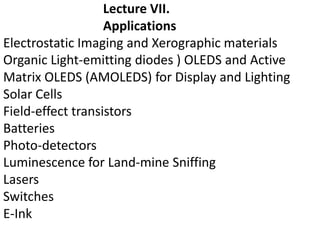
1. Lecture VII.
Applications
Electrostatic Imaging and Xerographic materials
Organic Light-emitting diodes ) OLEDS and Active
Matrix OLEDS (AMOLEDS) for Display and Lighting
Solar Cells
Field-effect transistors
Batteries
Photo-detectors
Luminescence for Land-mine Sniffing
Lasers
Switches
E-Ink
4. Limitations At Early Stage
Organic materials have often proved to be
unstable.
Making reliable electrical contacts to organic
thin films is difficult.
When exposed to air, water, or ultraviolet light,
their electronic properties can degrade rapidly.
The low carrier mobilities characteristic of
organic materials obviates their use in high-
frequency (greater than 10 MHz) applications.
These shortcomings are compounded by the difficulty of
both purifying and doping the materials.
10. History of Xerography
1906: Haloid Corp.
founded
1900 1910 1920 1930 1940 1950
1938: 1st
xerographic image
1949: 1st copier -
Model A
1950 1960 1970 1980 1990 2000
1959: Xerox 914, 1st plain paper
automatic copier - 7 1/2
copies/min
1964: LDX (long distance
xerography) - 1st fax
1973: Xerox 6500 -
1st color copier
1977: Xerox 9700 -
1st laser printer
1988: Xerox 5090 -
135 copies/min
1997: Docutech digital printer
(180 copies/min)
1997: Docucolor 70 - 70
color prints/min
Today Xerox has 91,400 employees (50,200 in US) and $18.2 billion in revenues
11. What is Xerography?
Creation of a visible image using surface charge pattern on a
“photoconductor”.
Visible images consist of fine charged particles called
toners”.
slide #5
Xero-graphy = Dry-Writing (Greek)
12. Xerographic Prints are composed of
toners
5-10 microns
COLORDigital prints are halftones
16. Charging Subsystem (Corotron):
Electrons
Positive Ions
Free ions are attracted
to wire; Free electrons are
repelled. Counter-charges
build up on grounded surfaces.
Rapidly moving electrons
and ions collide with air
molecules, ionizing them
and creating a corona.
Electrons continue to
follow Electric Field lines
to Photoreceptor until
uniform charge builds up
HV Power
Supply (-)
HV Power
Supply (-)
HV Power
Supply (-)
slide #10
17.
18.
19. Transfer to paper
• Electric field moves particles from
photoreceptor to paper or
transparency
• Detachment field must overcome
toner adhesion to photoreceptor
Apply E
Field
Paper
Paper
Photoreceptor
Photoreceptor
slide #18
21. Electrical Field Detachment of Fine
Particles
E. Eklund, W. Wayman, L. Brillson, D. Hays, 1994 IS&T Proc.,
10th Int. Cong. on Non-Impact Printing, 142-146
slide #19
Measure Many Particle Adhesion
Donor Receiver
V
transparent
conductive
electrodes
VV
22. Fusing Subsystem
• Permanently affix the image to the final substrate
– paper of various roughness
– transparency (plastic)
• Apply heat and/or pressure
Hot Roll
Fuser:
Pressure Roll
Heat Roll
Paper
slide #21
23. Cleaning and Erase Subsystems
• Removes unwanted residual toner and charge
from photoreceptor before next imaging cycle
– Physical agitation removes toner (blade or brush)
– Light neutralizes charge by making entire
photoreceptor conductive
slide #22
49. Future of Xerography
• Color: Wide gamut, offset quality
• High Image Quality: High resolution,
continuous tone
• High Speed: Full color at 200 pages per
min, and higher
• Higher reliability: No paper jams
• Lower cost: Xerography vs. inkjet
slide #25
57. Why Organic LED?
Vibrant colors
High contrast
Wide viewing angles from all directions
Low power consumption
Low operating voltages
Wide operating temperature range
A thin and lightweight form factor
Cost-effective manufacturability , etc
62. A full color, 13-inch diagonal small-molecular-weight OLED display with
2mm thickness.
Flexible internet display screen
S. R. Forrest in Nature428, 911 (2004)
Applications — Full color OLED display
63. Samsung large OLED displays
KODAK OLED displays
http://www.kodak.com/eknec/PageQuerier.jhtml?pq-path=1473/1481/1491&pq-locale=en_US
Applications — Full color OLED display
91. Cathode
Organic Layer
Anode
Substrate
Single layer device
Small molecular OLEDs — Structure
Cathode
Hole transport layer
Anode
Substrate
Electron transport layer
P-n junction device
Electron transport layer
Hole transport layer
Anode
Substrate
Emissive layer
Electron Injection layer
Cathode
Hole Injection layer
Multiple layers device
92. Electron transport layer
Hole transport layer
Anode
Substrate
Emissive layer
Electron Injection layer
Cathode
Hole Injection layer
HOMO — Ev
LUMO — Ec
Transparent
substrate
ITO HIL HTL EML ETL EIL Cathode
h+
e-
h+ h+
e-
e-Light
Electrons injected from cathode
Holes injected from anode
Transport and radiative recombination of
electron hole pairs at emissive layer
Small molecular OLEDs — Device operation principle
93.
94. Anode:
Indium-tin-oxide (ITO): 4.5-5.1 eV
Au: 5.1 eV
Pt: 5.7 eV
Cathode:
Ca: 2.9 eV
Mg: 3.7 eV
Al: 4.3 eV
Ag: 4.3 eV
Mg : Al alloys
Ca : Al Alloys
Small molecular OLEDs — Electrodes