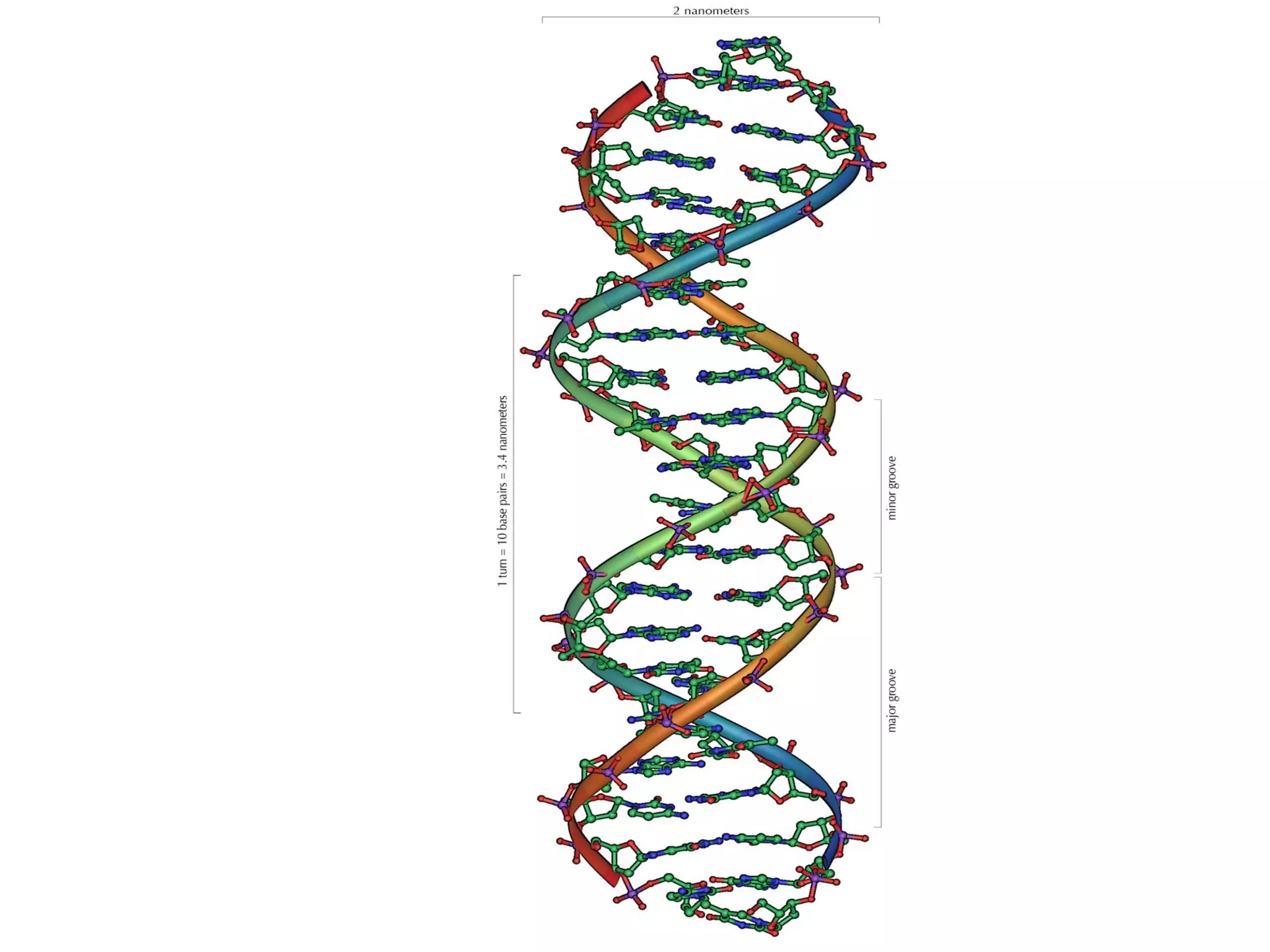
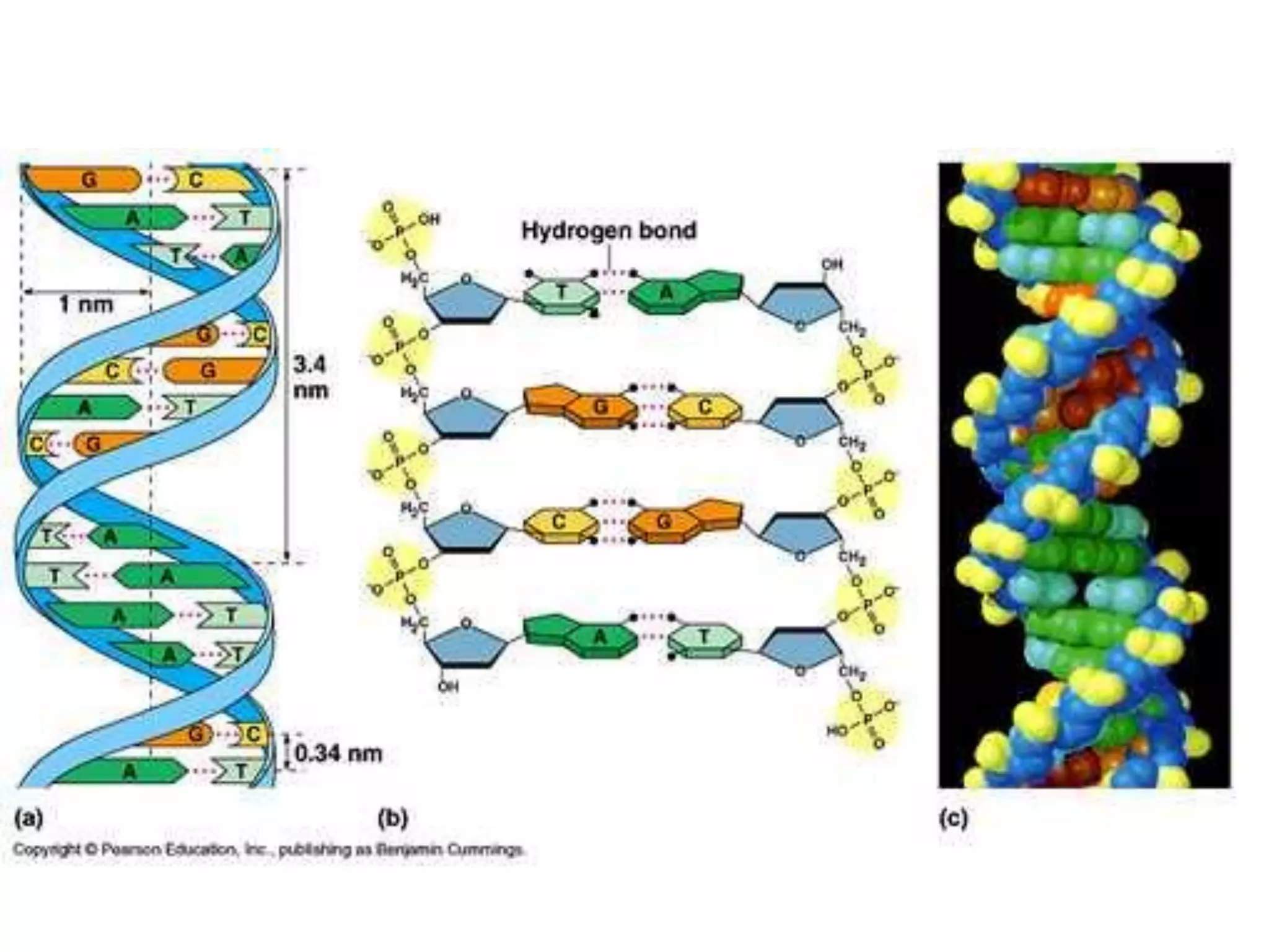
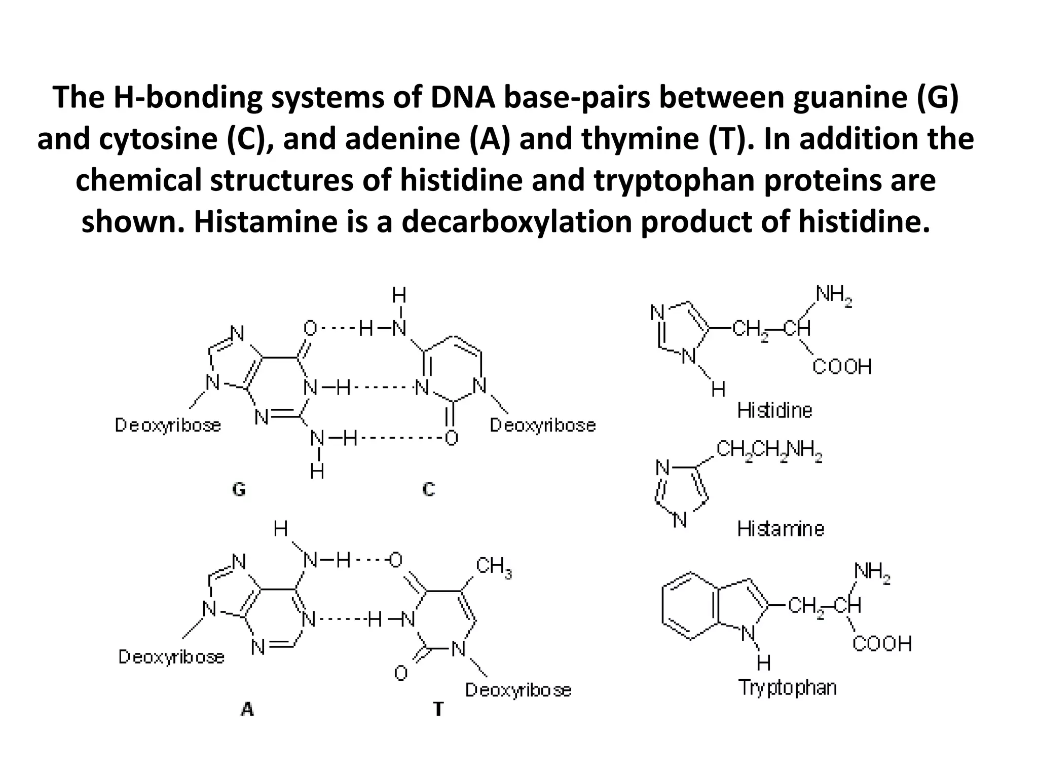
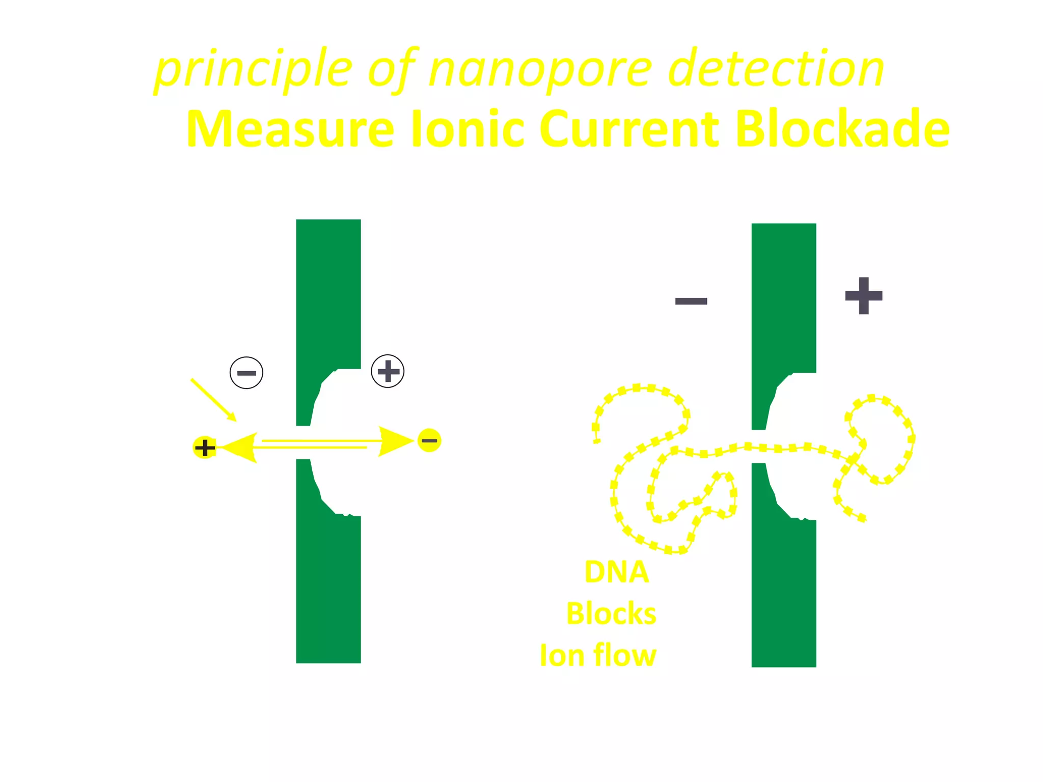
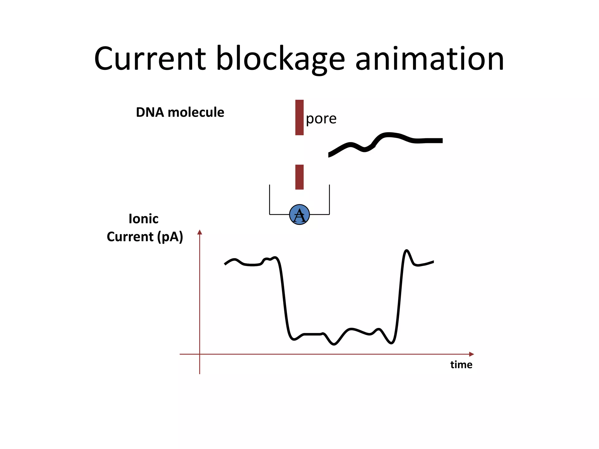
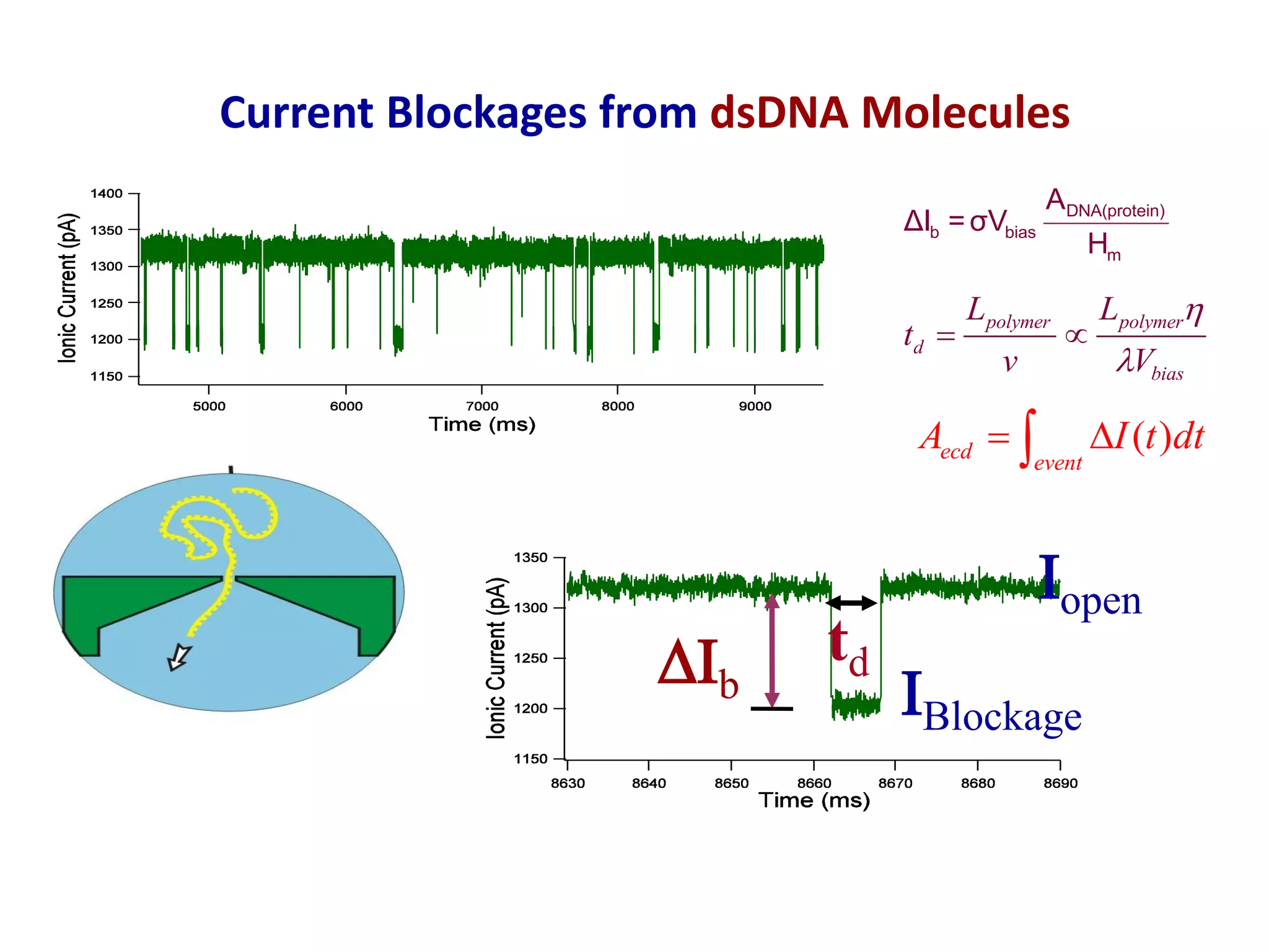
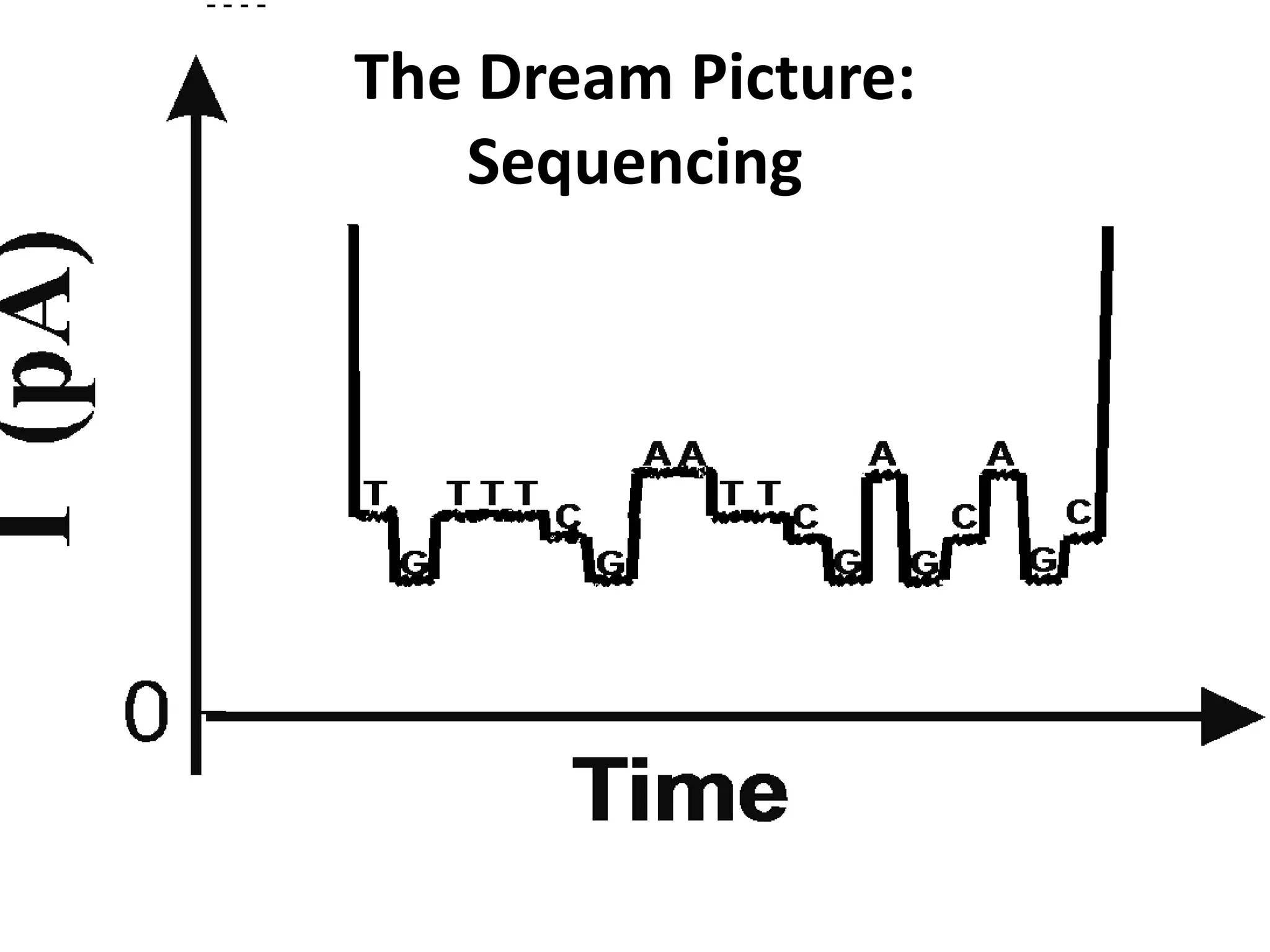
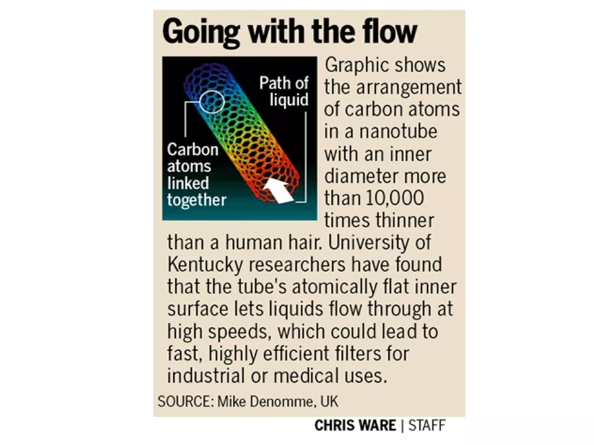
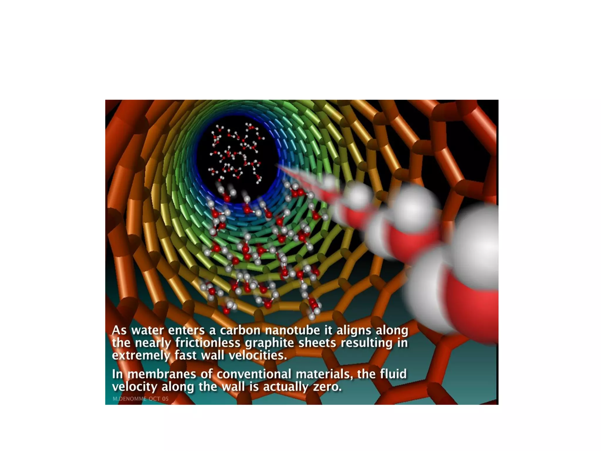
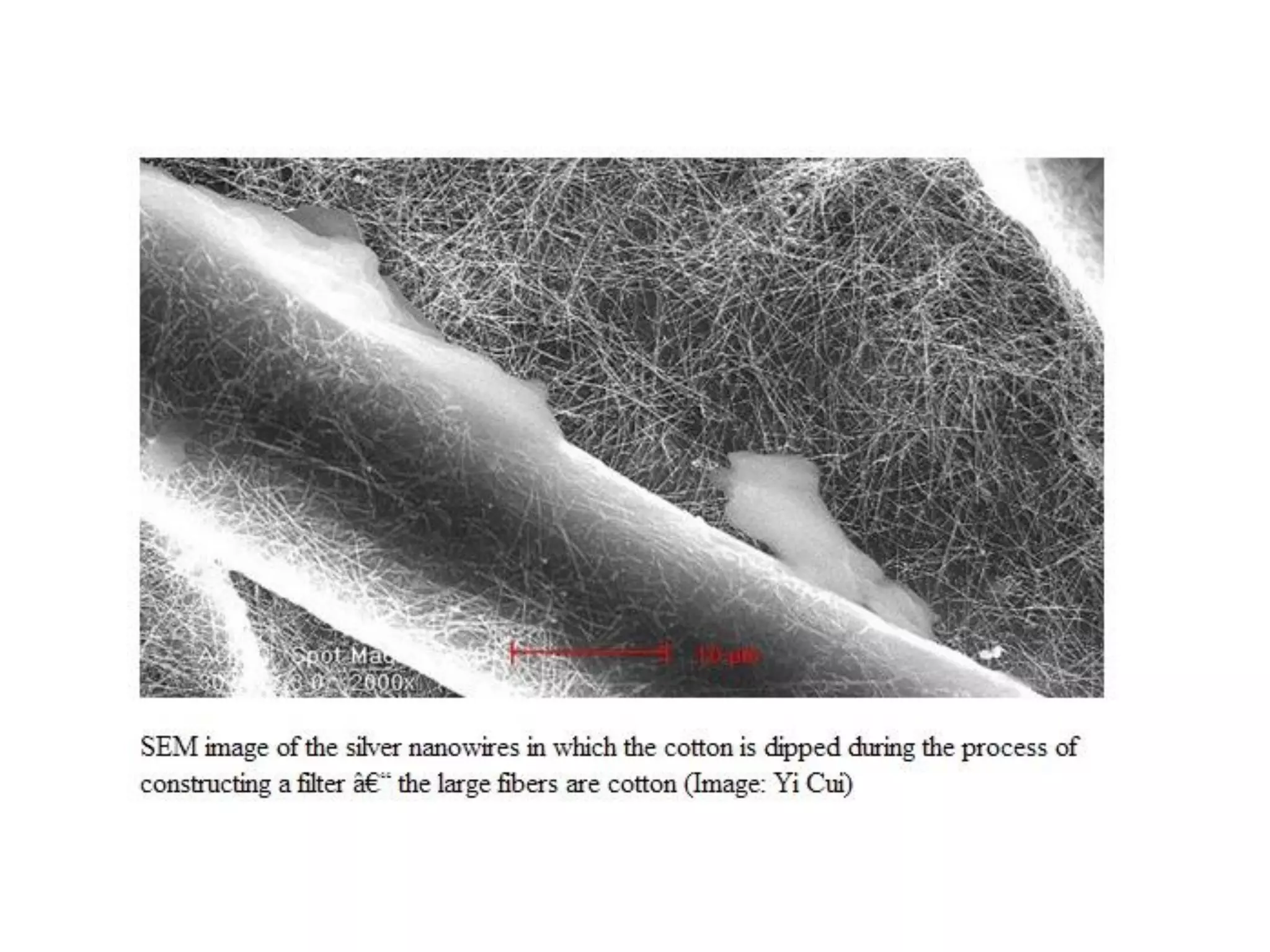
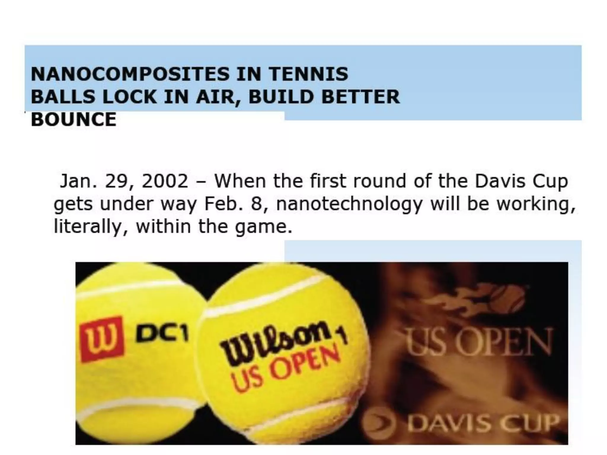
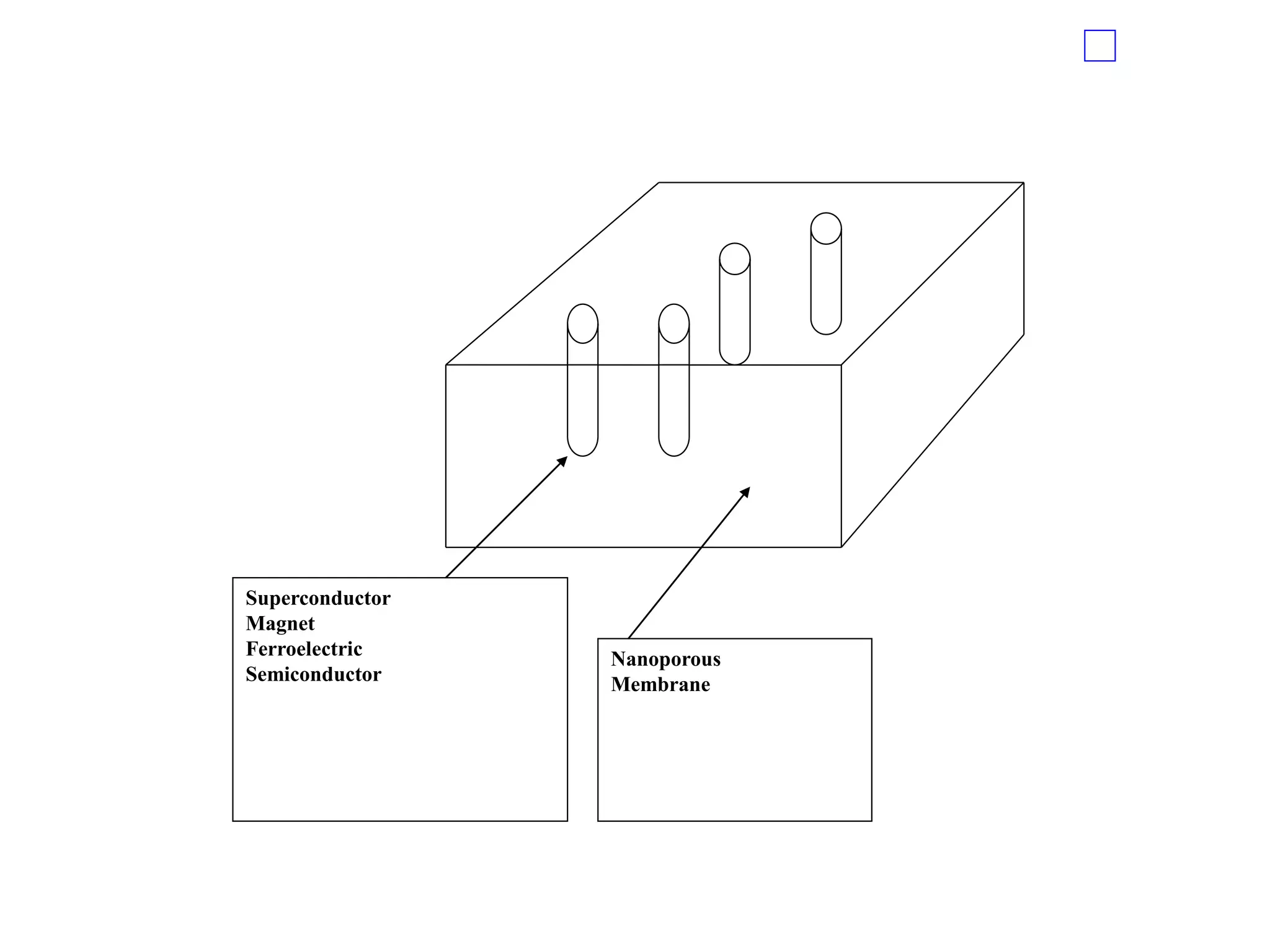
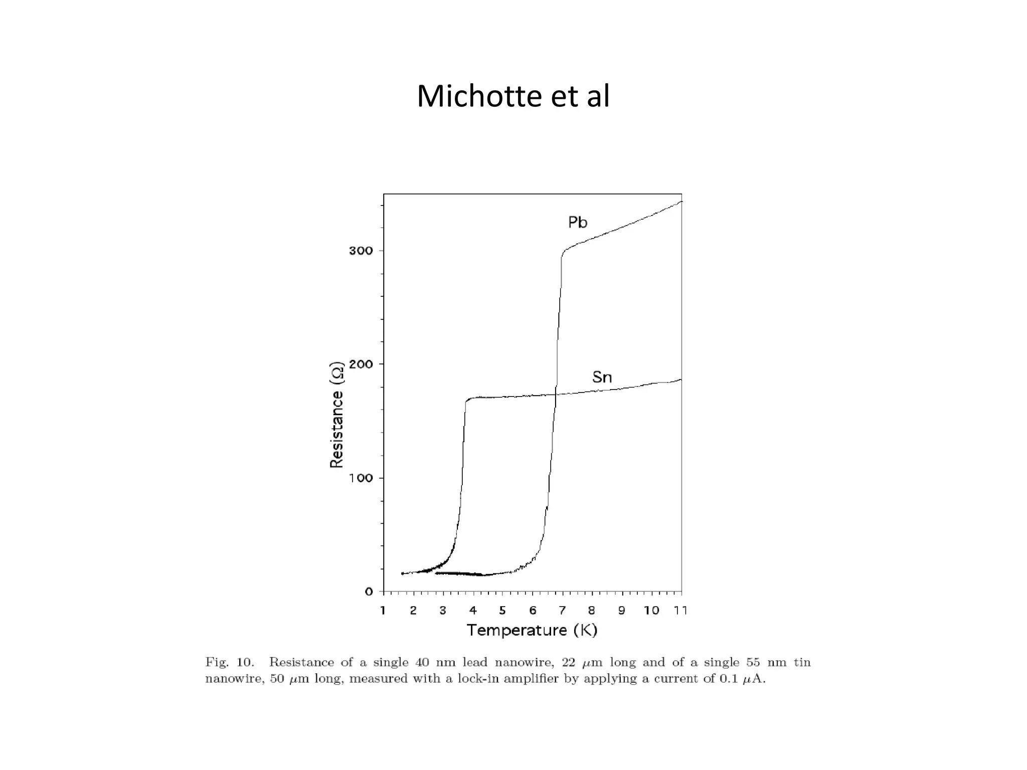
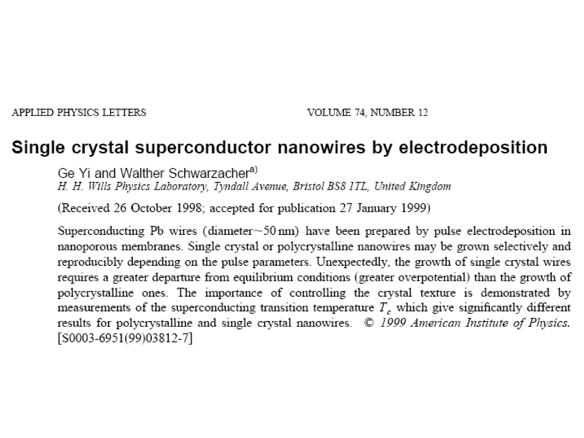
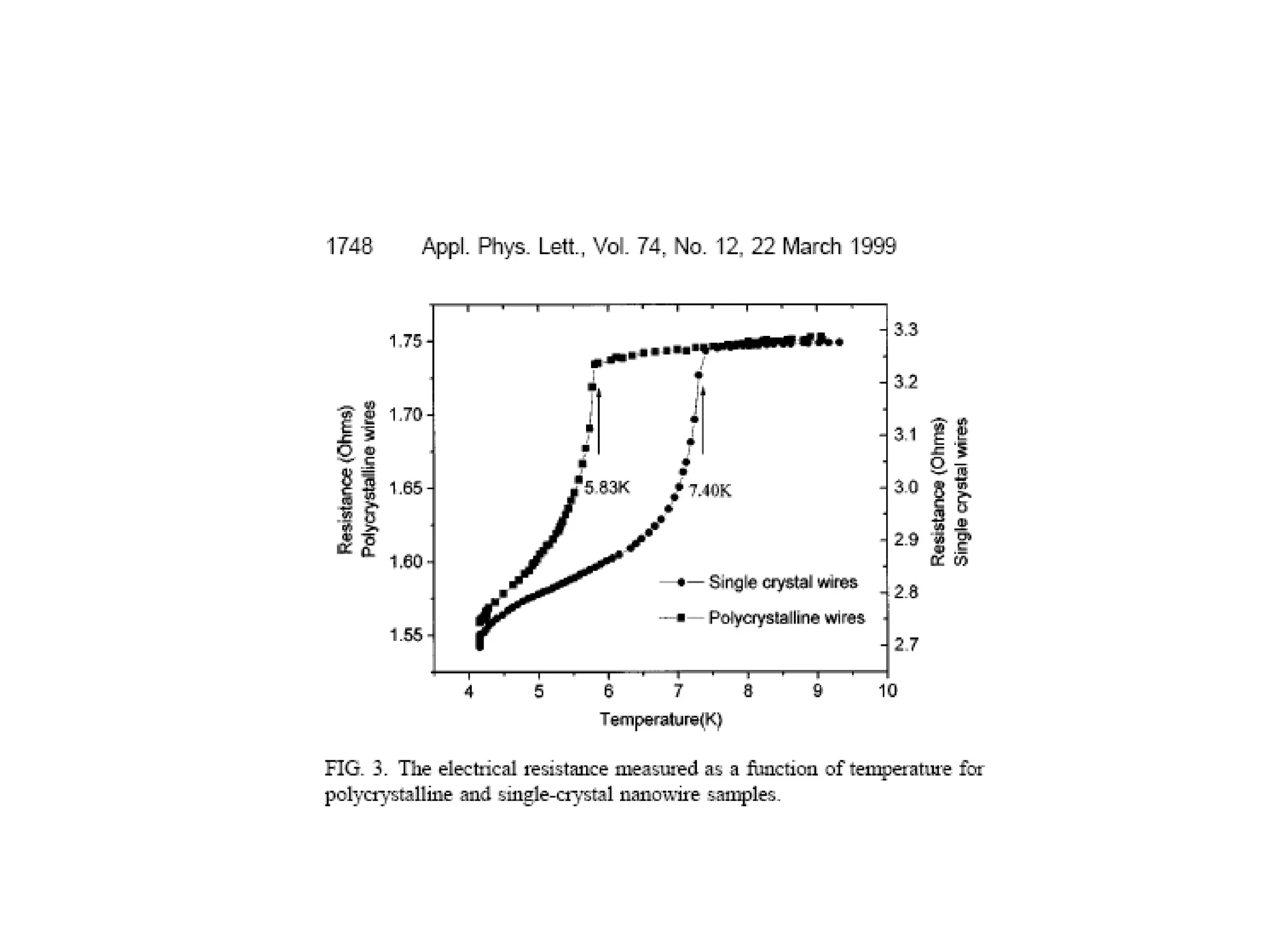
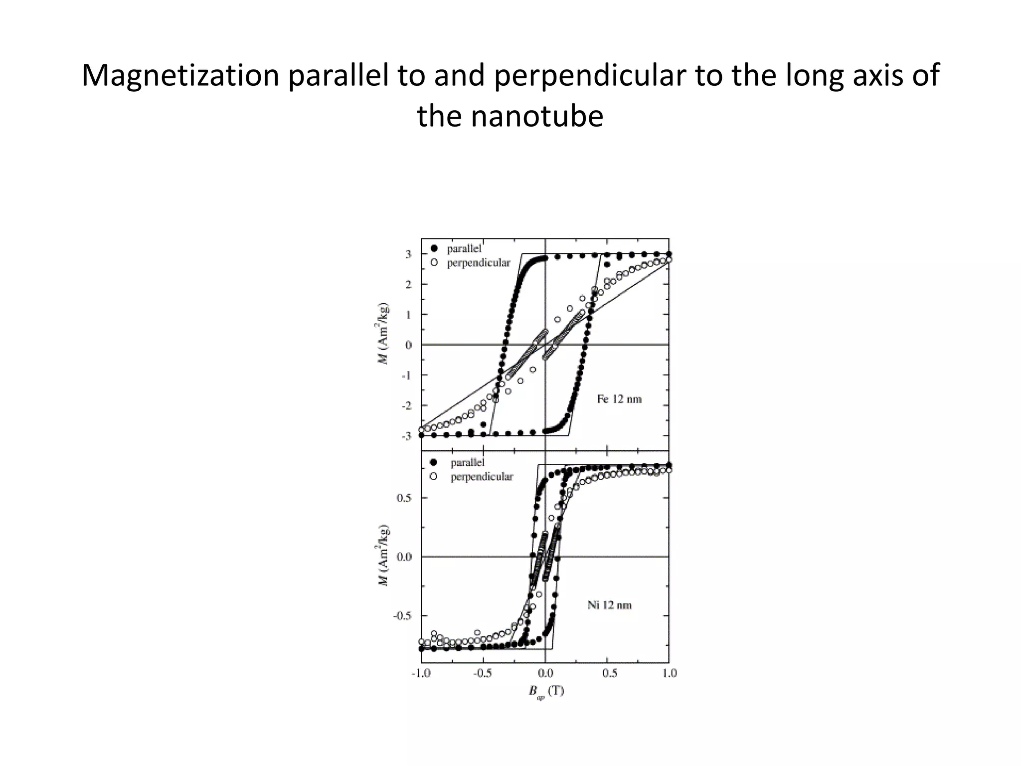
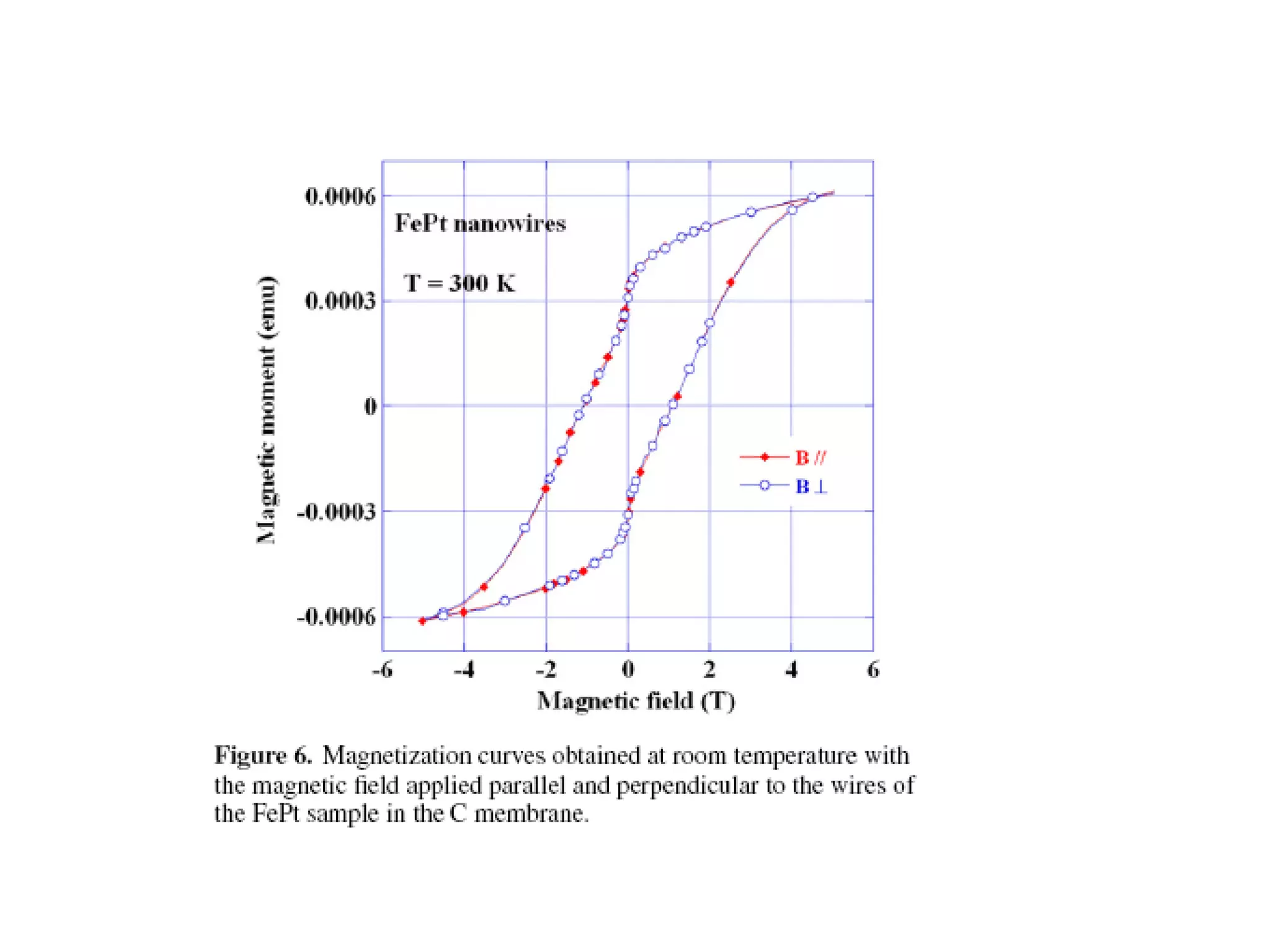
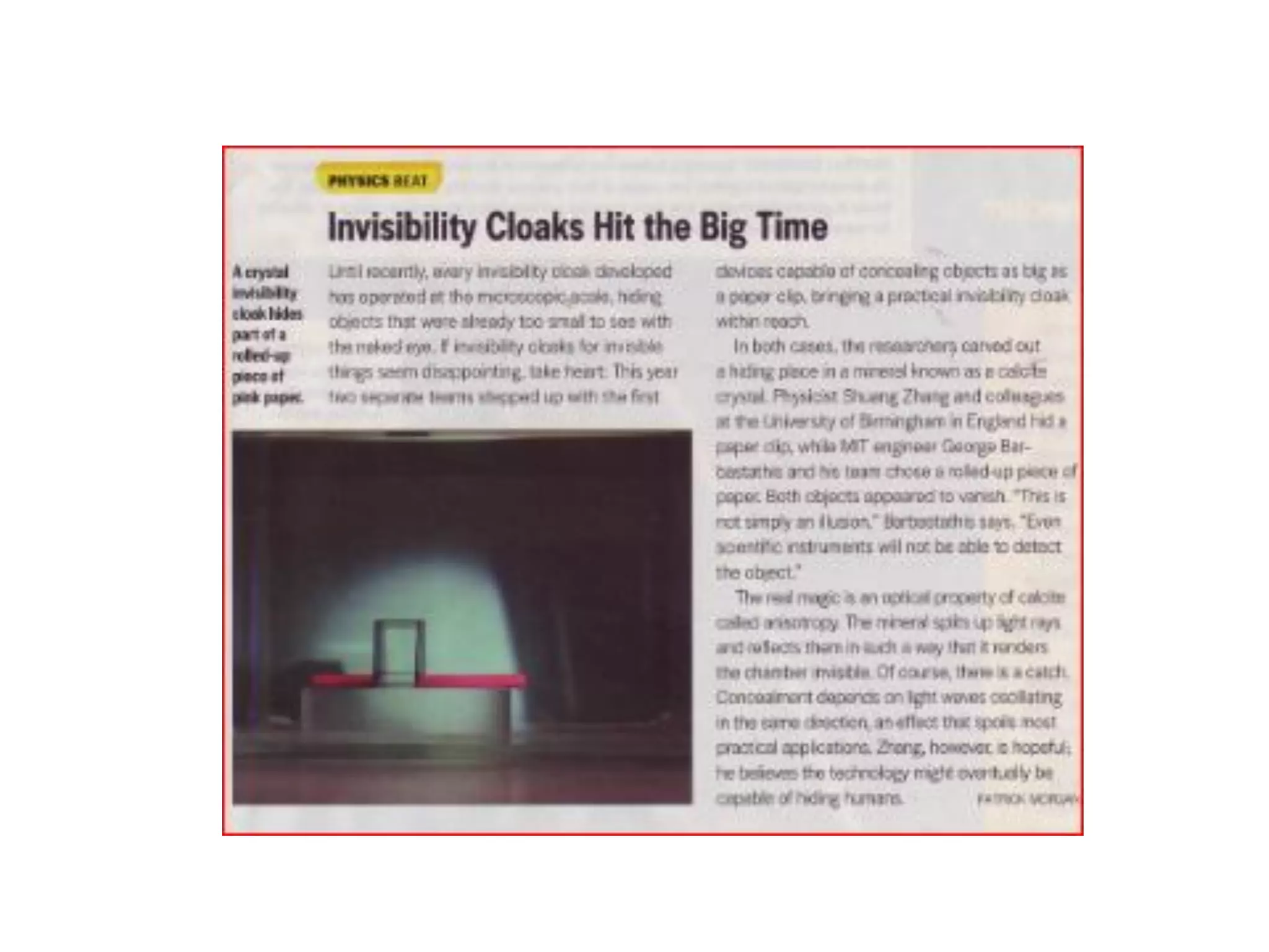
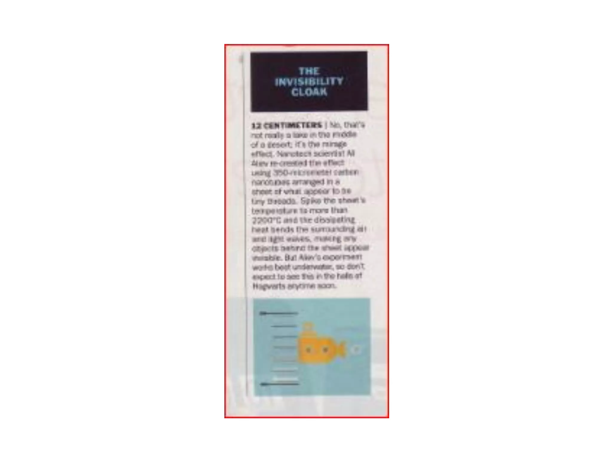
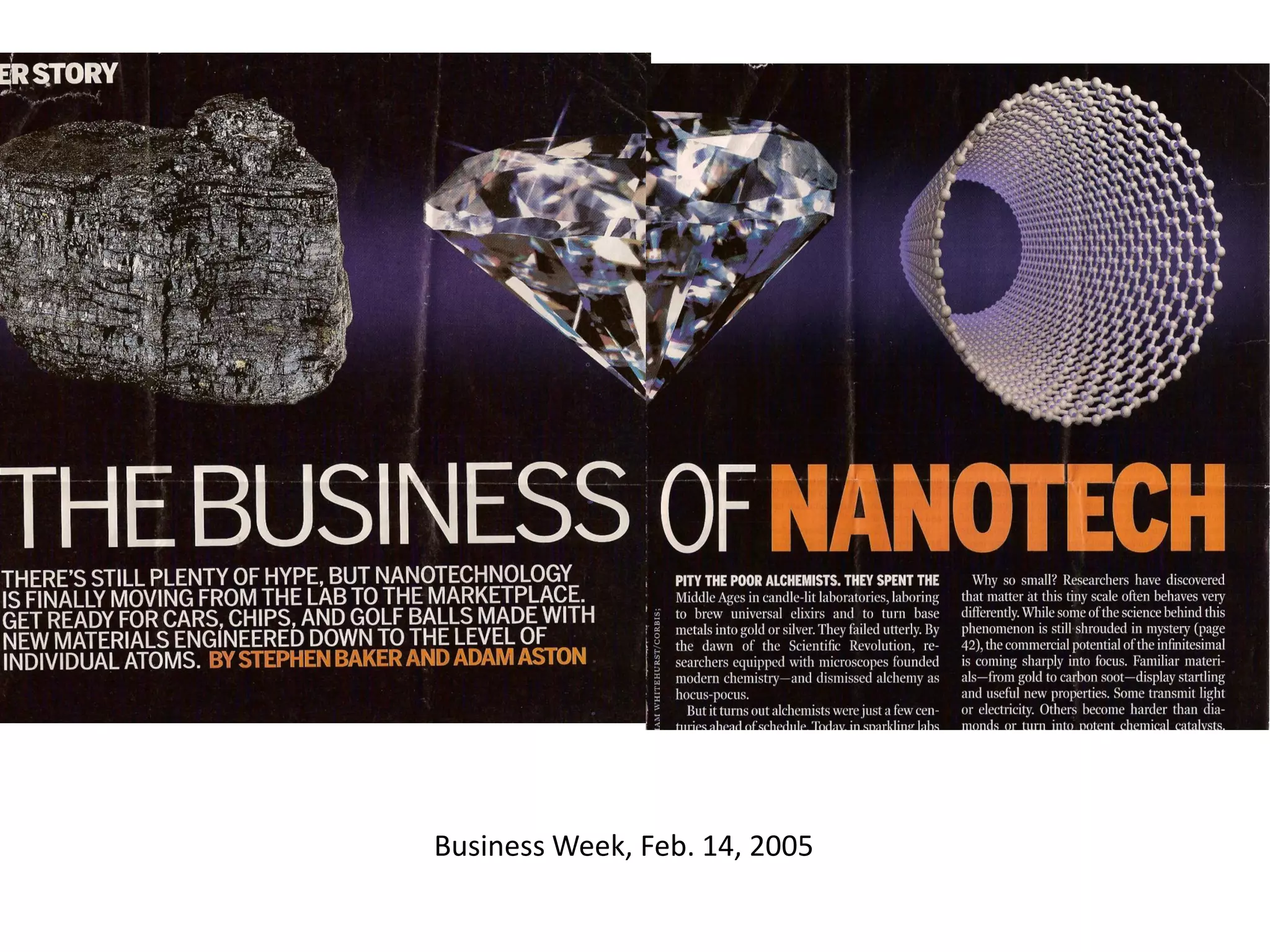
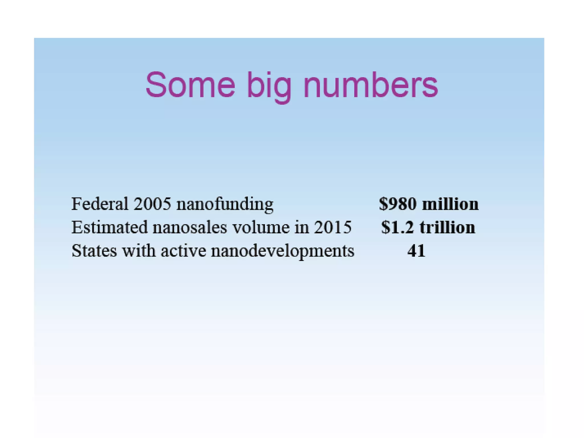
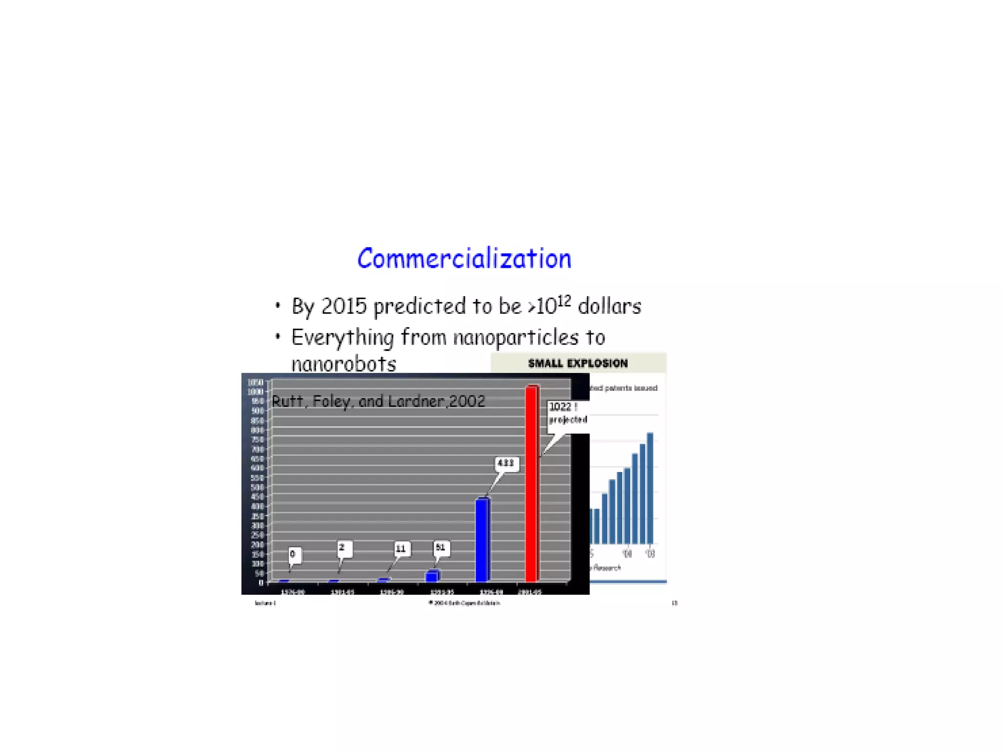
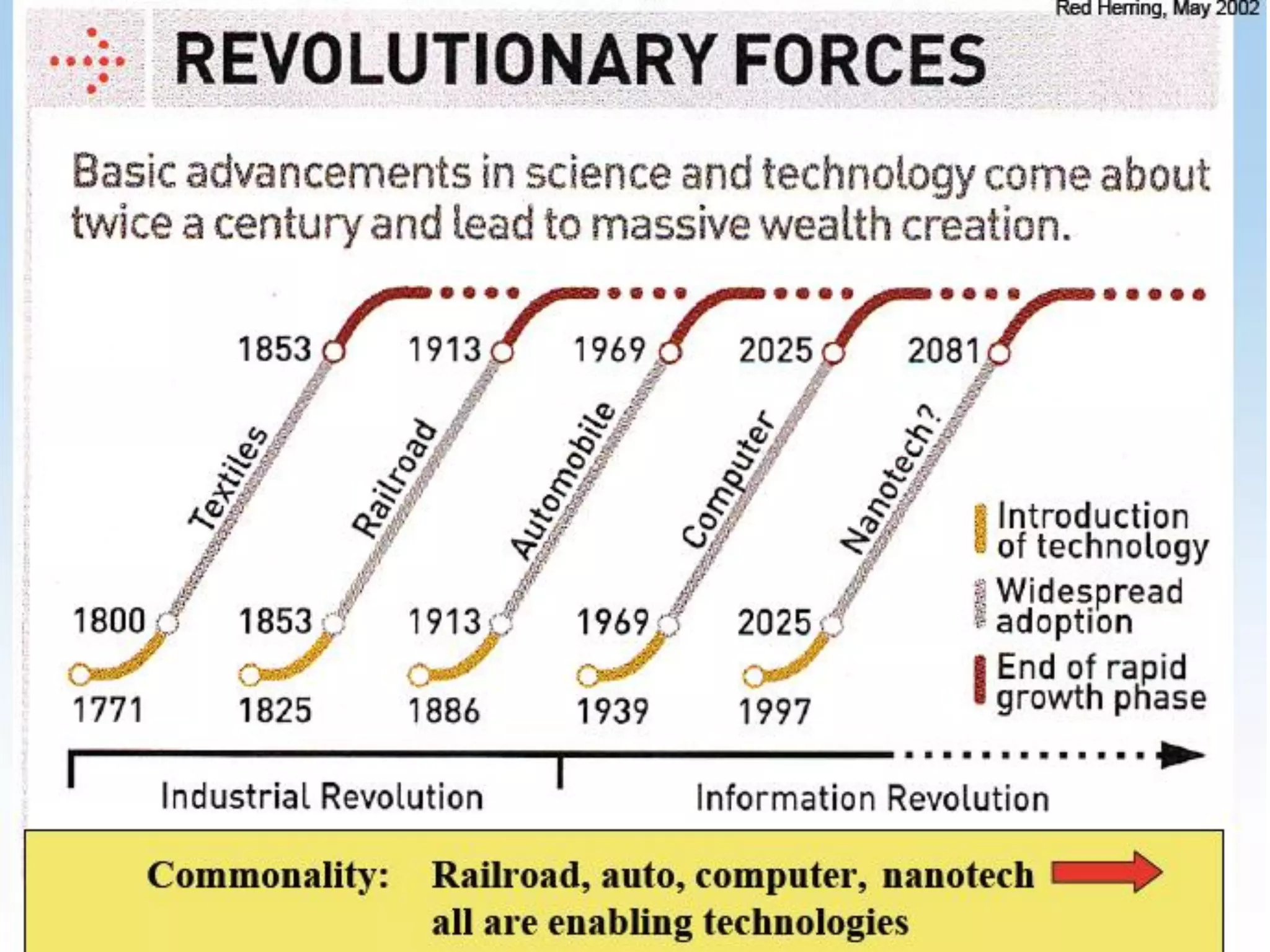
This document provides an overview of various nanotechnology applications including DNA sequencing using nanopores, filtration, uses in clothing and sports, composites, nanomedicine, superconductors, magnetic nanowires, ferroelectrics, and dielectric nanostructures. It also discusses the business of nanotechnology and provides examples of research on growing superconducting lead nanowires, fabricating yttrium barium copper oxide superconductor nanowires, investigating the magnetic properties of ferromagnetic nanowires, and developing ferroelectric nanotubes and metamaterials using dielectric nanostructures.


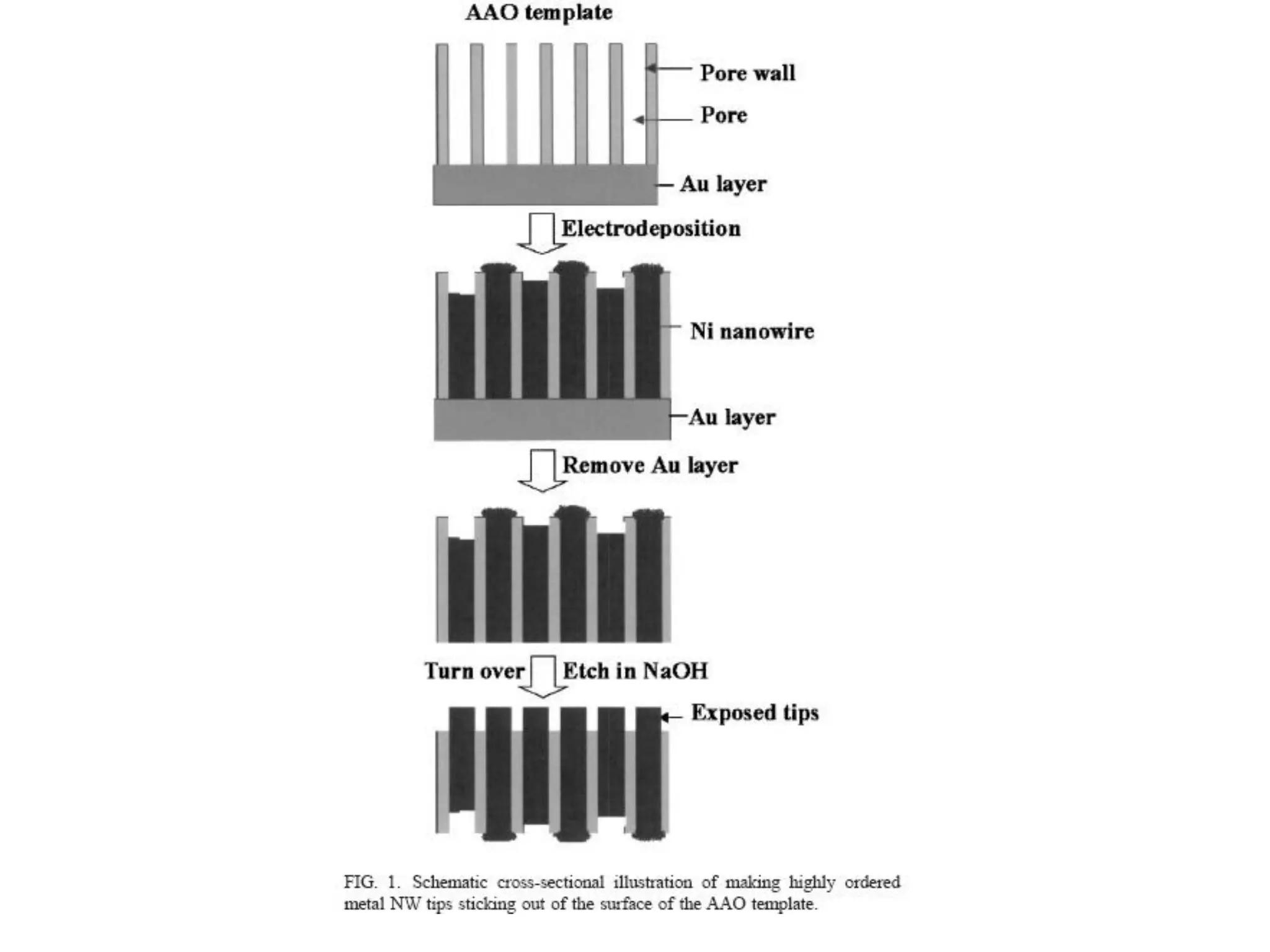
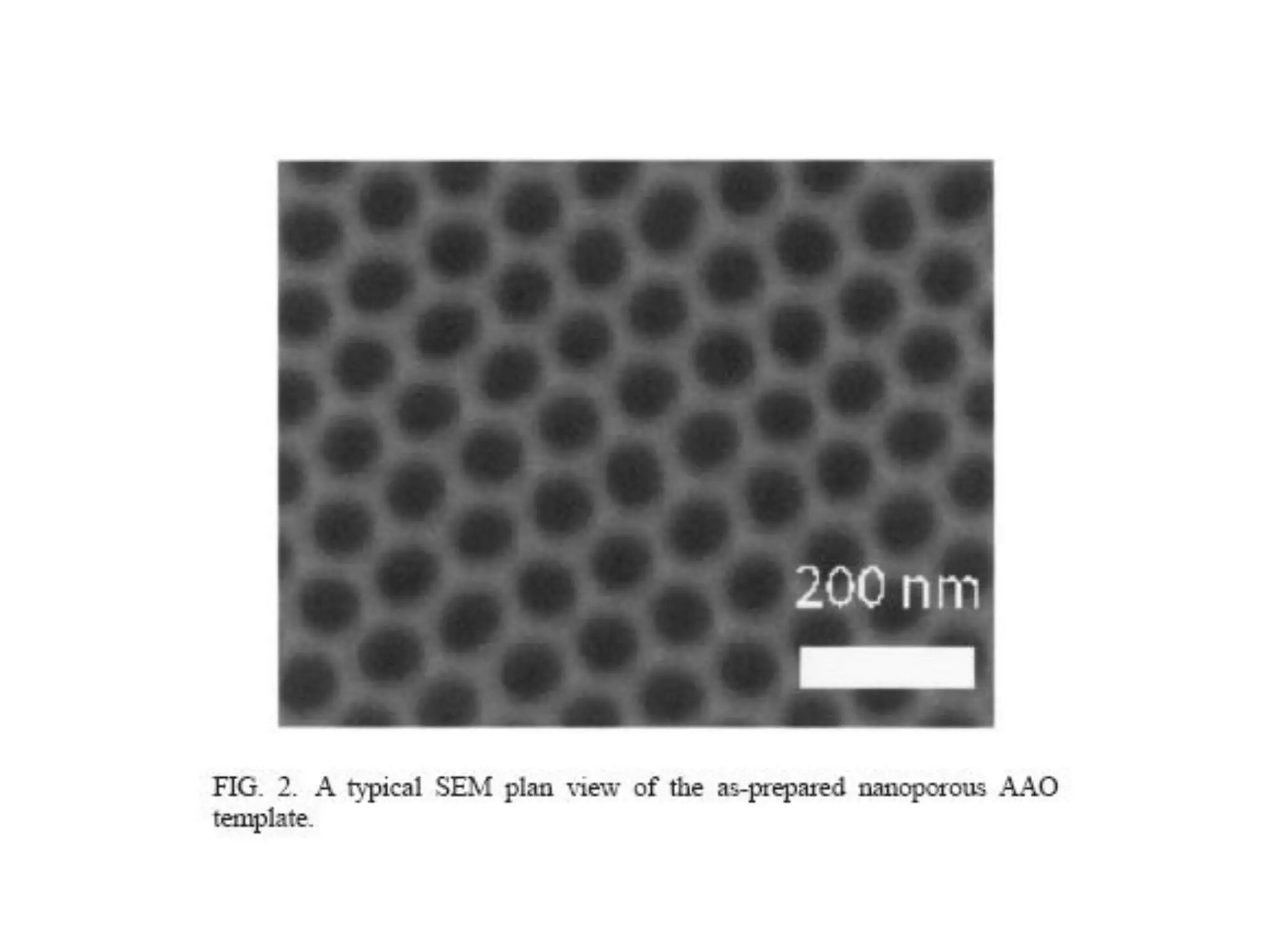
![• Preparation of anodic aluminum oxide (AAO) template
• Porous AAO membrane was prepared using a two-step anodizing process [19].
After degreasing in ethanol, high-purity Al foil (99.999%) was electropolished in a
H3PO4–H2SO4–H2O (40:40:20 wt.%) solution for 5 min to reduce the surface
roughness. The resulting Al sheet was washed with ethanol and distilled water,
then mounted on a copper plate to serve as anode for anodization. In the first
step, the anodizing of the Al sheet was carried out under constant voltages of 40 V
in 0.3 M oxalic acid electrolyte for 6 h at 17 °C. Prior to the second anodization,
first disordered porous alumina layer was removed in a mixture of H3PO4 (6 wt.%)
and CrO3 (1.8 wt.%) at 60 °C for 3 h. The second step was following the same
conditions as that of the first, except that the anodizing time was 3 h. A stepwise
voltage reduction technique [28 and 29] was then utilized to thin the barrier layer.
The as-obtained AAO membrane was immersed in 5 wt.% aqueous H3PO4 solution
for pore widening and barrier layer dissolving, followed by washing and drying.
Finally, the through-hole AAO membrane was detached from the Al substrate in a
saturated HgCl2 solution for next use.](https://image.slidesharecdn.com/2012tuslecture7-120501150500-phpapp01/75/2012-tus-lecture-7-45-2048.jpg)


![Ultra smooth and lattice relaxed zn o thin films [eid]](https://cdn.slidesharecdn.com/ss_thumbnails/ultra-smoothandlatticerelaxedznothinfilmseid-141105101210-conversion-gate02-thumbnail.jpg?width=640&height=640&fit=bounds)


