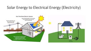
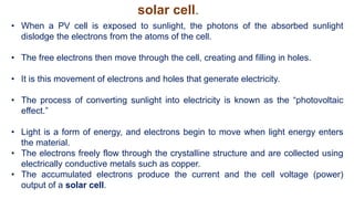
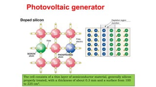
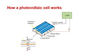
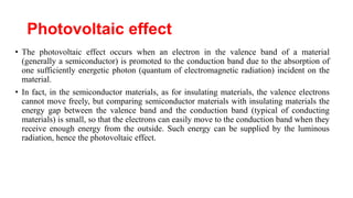
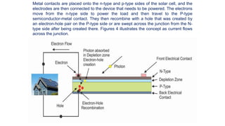
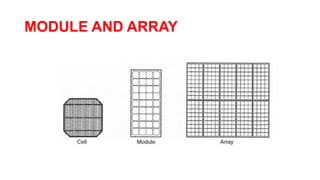
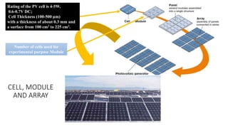
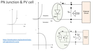
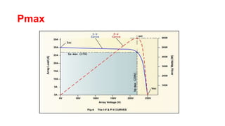
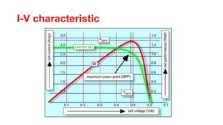
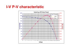
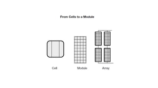
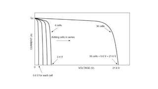
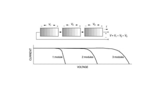
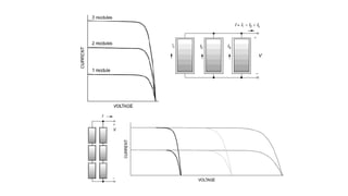
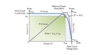
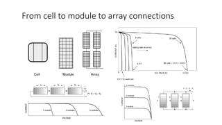
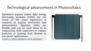
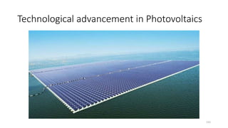
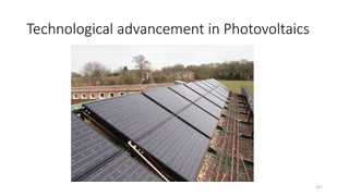
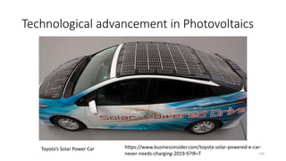
WIND AND SOLAR ENERGY
OPEN ELECTIVE SEMESTER 5
SCHOOL OF TECHNOLOGY
UNIT 3
SOLAR ENERGY CONVERSION SYSTEM
Dr. Bhinal Mehta
UNIT III: Solar Energy Conversion System
Solar Thermal Systems: Introduction, Solar Collectors.
Solar Water Heater, Solar Passive Space Heating & Cooling Systems.
Solar Industrial Heating Systems, Solar Refrigeration & Air Conditioning
Systems, Solar Cookers.
Solar Photovoltaic Systems: Solar Cell; Fundamentals of solar cell
Solar Cell Characteristics, Solar Cell Classification, Solar Cell Technologies
Solar Cell, Solar Module, Array, Maximizing, Solar PV Output & Load Matching.
Maximum Power Point Tracker, Balance of System Components, Applications.
Numerical on design
Solar Energy to Electrical Energy (Electricity)
• When a PV cell is exposed to sunlight, the photons of the absorbed sunlight
dislodge the electrons from the atoms of the cell.
• The free electrons then move through the cell, creating and filling in holes.
• It is this movement of electrons and holes that generate electricity.
• The process of converting sunlight into electricity is known as the “photovoltaic
effect.”
• Light is a form of energy, and electrons begin to move when light energy enters
the material.
• The electrons freely flow through the crystalline structure and are collected using
electrically conductive metals such as copper.
• The accumulated electrons produce the current and the cell voltage (power)
output of a solar cell.
solar cell.
PV Cell
• The physics of the PV cell is very similar to that of the classical diode
with a PN junction.
• When the junction absorbs light, the energy of absorbed photons is
transferred to the electron–proton system of the material, creating
charge carriers that are separated at the junction.
• The charge carriers may be electron–ion pairs in a liquid electrolyte or
electron–hole pairs in a solid semiconducting material.
• Typical rating of such cell is 3W, 0.5V DC generally.
Basic construction of PV cell with performance-enhancing features
Photovoltaic effect and PN Junction
https://www.pveducation.org/pvcdrom/solar-cell-operation/the-photovoltaic-effect
Valance Band
Conduction Band
The highest energy level that an electron can occupy at the absolute zero temperature is known as the Fermi
Level. The Fermi level lies between the valence band and conduction band because at absolute zero
temperature the electrons are all in the lowest energy state. Due to the lack of sufficient energy at 0 Kelvin, the
Fermi level can be considered as the sea of fermions (or electrons) above which no electrons exist. The Fermi
level changes as the solids are warmed and as electrons are added to or withdrawn from the solid.
The Fermi level of a solid-state body is the thermodynamic work required to add one electron to the body. It is a
thermodynamic quantity usually denoted by µ or EF for brevity.
The Portion of the Periodic Table of Greatest
Importance for Photovoltaics Includes the
Elements Silicon, Boron, Phosphorus, Gallium,
Arsenic, Cadmium, and Tellurium
Boron And Phosphorus, From Groups III And
V, Are Added To Silicon To Make Most PVs.
Gallium And Arsenic are used In GaAs Solar
Cells, While Cadmium And Tellurium Are Used
In CdTe Cells
Silicon Electron Transport
A silicon atom has 14 electrons arranged
in three different shells. The first two shells
are full, and the third shell is partially
empty, having only four electrons as
shown in Figure 1. An atom in its ideal
state needs eight electrons in its last shell.
Therefore, to compensate for the empty
spaces, it shares four electrons with its
neighboring silicon atoms (this is what
forms the crystalline structure). The
material properties of silicon in its “pure”
state allows it to be a conductor because
its electrons are unable to move around
(they are locked in this crystalline
structure).
Therefore, the silicon material properties need to be modified to allow the electrons to
move around. This task is accomplished by implanting impurities into the silicon
material. When other types of atoms are mixed into the material, this enables the
electrons to move. For example, a phosphorous atom has five electrons in its outer
shell, and if these are placed into the silicon material, it still bonds with the silicon atoms,
but there is one free electron that is not bonded.
Silicon has 14 protons in its nucleus, and so it has 14 orbital electrons as well. As
shown in Fig. a, its outer orbit contains four valence electrons—that is, it is
tetravalent. Those valence electrons are the only ones that matter in electronics, so
it is common to draw silicon as if it has a +4 charge on its nucleus and four tightly
held valence electrons, as shown in Fig. b.
Pure crystalline silicon, each atom forms covalent bonds with four
adjacent atoms in the three-dimensional tetrahedral pattern shown in
Fig. a. For convenience, that pattern is drawn as if it were all in a
plane, as in Fig. b.
Some basic characteristics of PV material
• At absolute zero temperature, silicon is a perfect electrical insulator. There are
no electrons free to roam around as there are in metals.
• As the temperature increases, The warmer it gets, the more electrons there are
to carry current, so its conductivity increases with temperature (in contrast to
metals, where conductivity decreases).
• Electrons have energies that must fit within certain allowable energy bands.
• At room temperature, only about one out of 1010 electrons in silicon exists in
the conduction band.
Energy bands for (a) metals and (b) semiconductors. Metals have
partially filled conduction bands, which allows them to carry
electric current easily. Semiconductors at absolute zero
temperature have no electrons in the conduction band, which
makes them insulators at absolute zero temperature.
A photon with sufficient energy can create a
hole–electron pair as in (a). The electron can
recombine with the hole, releasing a photon of
energy (b).
When a hole is filled by a nearby valence electron, the hole
appears to move.
The important point here is that electric current in a semiconductor can be carried not only by
negatively charged electrons moving around, but also by positively charged holes that move
around as well.
• Photons with enough energy create hole–electron pairs in a semiconductor.
• Photons can be characterized by their wavelengths or their frequency as well as by their
energy; the three are related by the following:
c = λν
• where c is the speed of light (3 × 10⁸ m/s), v is the frequency (hertz), λ is the wavelength (m),
and
E = hν = hc / λ
• Where, E is the energy of a photon (J) and h is Planck’s constant (6.626 × 10⁻³⁴ J-s).
Photons with wavelengths above 1.11 μm don’t have the 1.12
eV needed to excite an electron, and this energy is lost.
Photons with shorter wavelengths have more than enough
energy, but any energy above 1.12 eV is wasted as well.
Solar spectrum at AM 1.5. Photons with wavelengths longer than 1.11 μm
don’t have enough energy to excite electrons (20.2% of the incoming solar
energy); those with shorter wavelengths can’t use all of their energy, which
accounts for another 30.2% unavailable to a silicon photovoltaic cell.
Spectrum is based on ERDA/NASA (1977).
Photovoltaic generator
The cell consists of a thin layer of semiconductor material, generally silicon
properly treated, with a thickness of about 0.3 mm and a surface from 100
to 225 cm2.
How a photovoltaic cell works
Photovoltaic effect
• The photovoltaic effect occurs when an electron in the valence band of a material
(generally a semiconductor) is promoted to the conduction band due to the absorption of
one sufficiently energetic photon (quantum of electromagnetic radiation) incident on the
material.
• In fact, in the semiconductor materials, as for insulating materials, the valence electrons
cannot move freely, but comparing semiconductor materials with insulating materials the
energy gap between the valence band and the conduction band (typical of conducting
materials) is small, so that the electrons can easily move to the conduction band when they
receive enough energy from the outside. Such energy can be supplied by the luminous
radiation, hence the photovoltaic effect.
• When a photon hits a piece of silicon, it can either be absorbed by the silicon,
reflect off of the surface, or pass through the silicon.
• The photon path depends on whether the photon energy is higher or lower than
the band gap.
• If the photon is absorbed, its energy is given to an electron in the crystal lattice.
• The valence electron is usually bonded tightly due to neighboring atoms;
however, the additional energy provided by the photon excites it into the
conduction band, where it can move around in the semiconductor.
• The electron moves to another location (hole) and leaves a “hole” where it once
was.
• This phenomenon is called mobile “electron-hole” pairs in the semiconductor.
• Photo generation of Charge Carriers
• Since PV materials only absorb a certain range of energies, certain wavelengths
of light will be unable to create free electrons.
• Depending upon the material type, a certain amount of energy (1.1 eV for
crystalline silicon) is required to make electrons move; this is known as the “the
band gap energy” of the material.
The band gap also determines the strength (voltage) of the electric field. If it is too
low, the extra absorbed photons do not create a high enough voltage to produce
the required power. There are also electron losses due to the contact area between
the metal and material. Theoretically, the larger the metal contact, the more
electrons it can collect. However, a significant portion of the material cannot be
covered because light needs to enter the material to generate the electric current.
Also, silicon is a semiconductor (not a conductor), which means that it is difficult for
electrons to travel through the material due to the high internal resistance. The
optimal band gap is 1.4 eV for a cell material to balance these two effects.
Silicon and the P-N Junction
When energy is added to pure silicon, a few electrons break free from the
lattice – which leaves a “hole.” These free electrons then attempt to become
stable by looking for another hole. These free electrons are termed “free
carriers.” The silicon with the extra phosphorous electrons (doped) allows
enough electrons to move to be able to conduct current. The process of
adding electrons is called “doping,” and the silicon materials with the
phosphorous atoms is termed “n-type silicon.” Silicon material can also be
doped with boron, which has only three electrons in its outer shell compared
with the four that silicon has. This type of silicon is called “p-type,” and
therefore, silicon has free “holes” instead of electrons. These “holes” move
around like the electrons and carry a positive charge. If p-type silicon is
placed into contact with n-type silicon, then the electrons will diffuse from a
region of high concentration (n-type side) to a region of low concentration (p-
type side). The electrons in the n-type material are repelled by the negative
electrode and are drawn to the p-type electrode. The holes in the p-type
material move the opposite way.
When the difference in voltage between the electrodes is high, the electrons in the
depletion zone come out of their holes and begin moving freely again. The depletion
zone disappears, and the charge moves across the diode. Figure 3 illustrates the P-N
junction before and after the electrons begin to move.
Metal contacts are placed onto the n-type and p-type sides of the solar cell, and the
electrodes are then connected to the device that needs to be powered. The electrons
move from the n-type side to power the load and then travel to the P-type
semiconductor-metal contact. They then recombine with a hole that was created by
an electron-hole pair on the P-type side or are swept across the junction from the N-
type side after being created there. Figures 4 illustrates the concept as current flows
across the junction.
Crystalline Silicon
The material most frequently used for PV panels is crystalline silicon, which has an
efficiency of approximately 15%. It can be made from a silicon ingot, ribbon, or wafer.
Monocrystalline silicon is usually formed using the Czochralski process.
These panels are expensive because they are made of pure cylindrical ingots. Figure
6 shows the basic steps in the forming solar modules.
Figure 6. Material steps in forming solar modules.
Solar Cell Classification
Particulars Monocrystalline Polycrystalline Mono-PERC Thin-film
Cost High Medium Highest Lower
Efficiency High Medium Highest Less
Appearance
Black/ Darker
colour with
octagonal shape
Blue colour with
square edges
Black and rounded
edges
Depends on the
variant
Advantages
Energy efficient
Heat resistant
Affordable
Less wastage
Most efficient
Less space
required
Lowest installation
cost
Lightweight
Disadvantages
Expensive
High carbon
footprint
Low heat
resistance
Lower energy
efficiency
Most expensive
Shorter life span
Lower efficiency
Comparison of Types of Solar Panels on Cost, Efficiency & Appearance
Passivated Emitter and Rear Cell (PERC) Solar Panels
Since an individual cell produces only about 0.5 V, a single cell is
practically of no use, apart from extra low power appliances.
Instead, the basic building block for PV applications is
a module consisting of several prewired cells in series, all
encased in tough, weather-resistant packages.
A typical module has 60 or 72 cells in series. The 72-cell modules
can be field-wired to act either as one 24-V module with all 72
cells in series or as 12-V modules with two parallel strings having
36 series cells in each. Multiple modules, in turn, can be wired in
series to increase voltage and in parallel to increase current, to
produce high power. An important element in PV system design is
deciding how many modules should be connected in series (a set
of PV modules in series is named a string) and how many in
parallel to deliver whatever energy is needed. Such combinations
of modules are referred to as an array.
CELL, MODULE AND ARRAY
MODULE AND ARRAY
CELL, MODULE
AND ARRAY
Rating of the PV cell is 4-5W,
0.6-0.7V DC;
Cell Thickness (100-500 µm)
with a thickness of about 0.3 mm and
a surface from 100 cm2 to 225 cm2.
Number of cells used for
experimental purpose Module
• Many PV cells are connected to form modules, which are then assembled into
larger units called arrays to increase the power output.
• These units of PV cells allow designers to build PV systems with customized
power output for different applications.
• A complete PV system consists of
 PV modules,
 support structures,
 wiring,
 storage,
 power conversion,
 power electronics devices.
About PN Junction
• When one can join a P-type material and the N-type material to produce a PN junction,
• The Fermi levels become equal and as a result the band bends like so.
• Essentially, if the light has energy bigger than the band gap energy, then it knocks an electron
off its site in a particular atom, makes it freely moveable in the bulk material.
• As a result, the electron goes to the conduction band, leaves behind a hole which is also free
to move that is in the valence band.
https://www.pveducation.org/pvcdrom/solar-cell-operation/light-generated-current
PN Junction & PV cell a
k
Vak
Power Flow
i
Sink
External
Circuit
Dissipation
Generation
Vak
i
Vak
i
a
k
Vak
Power
Flow
i
Source
External
Circuit
ip
id
https://pveducation.org/pvcdrom/solar-
cell-operation/iv-curve
Diode
Current
The Reverse Saturation
Current
Voltage Across The
Diode Terminals From
The P-side To The N-
side
The Electron
Charge (1.602 ×
10−19c)
Boltzmann’s
Constant (1.381 ×
10−23 J/K)
T Is The
Junction
Temperature
(K)
A current balance at a point to the left of Rps as shown in Fig., and with the Shockley diode equation for the currents
through the resistors and diode, yields the model characteristic equation:
where
• VPV = PV module voltage (V)
• IPV = PV module current (A)
• Iph = light current (A)
• I0 = diode reverse saturation current (A)
• Qd = diode ideality factor
• ns = number of cells in series
• Rs = series resistance (Ω)
• Rp = shunt resistance (Ω)
• Vt = kTc/q is the thermal voltage (V), k is Boltzmann's constant, Tc is the cell temperature, and q is the
charge of an electron.
Equivalent circuit
Solar Array Parameters
•VOC = open-circuit voltage: – This is the maximum voltage that the array provides when the terminals are not
connected to any load (an open circuit condition). This value is much higher than Vmp which relates to the
operation of the PV array which is fixed by the load. This value depends upon the number of PV panels connected
together in series.
•ISC = short-circuit current – The maximum current provided by the PV array when the output connectors are
shorted together (a short circuit condition). This value is much higher than Imp which relates to the normal
operating circuit current.
•MPP = maximum power point – This relates to the point where the power supplied by the array that is connected
to the load (batteries, inverters) is at its maximum value, where MPP = Imp x Vmp. The maximum power point of a
photovoltaic array is measured in Watts (W) or peak Watts (Wp).
•FF = fill factor – The fill factor is the relationship between the maximum power that the array can actually provide
under normal operating conditions and the product of the open-circuit voltage multiplied by the short-circuit current,
( VOC x ISC ) This fill factor value gives an idea of the quality of the array and the closer the fill factor is to 1 (unity),
the more power the array can provide. Typical values are between 0.7 and 0.8.
•%eff = percent efficiency – The efficiency of a photovoltaic array is the ratio between the maximum electrical
power that the array can produce compared to the amount of solar irradiance hitting the array. The efficiency of a
typical solar array is normally low at around 10-12%, depending on the type of cells (monocrystalline,
polycrystalline, amorphous or thin film) being used.
The short-circuit current and the open-circuit voltage are the maximum current
and voltage respectively from a solar cell. However, at both of these operating
points, the power from the solar cell is zero. The "fill factor", more commonly
known by its abbreviation "FF", is a parameter which, in conjunction with Voc and
Isc, determines the maximum power from a solar cell. The FF is defined as the
ratio of the maximum power from the solar cell to the product of Voc and Isc so
that:
Fill Factor
Graphically, the FF is a measure of the "squareness" of the solar cell and is
also the area of the largest rectangle which will fit in the IV curve. The FF is
illustrated below.
The maximum power point (MPP) corresponds to the biggest
rectangle that can fit beneath the I –V curve. The fill factor (FF) is
the ratio of the area (power) at MPP to the area formed by a
rectangle with sides VOC and ISC.
Fill factors around 70–75% for crystalline silicon solar modules
are typical, while for multi junction amorphous-Si modules, it is
closer to 50–60%.
The I –V curve and P-V curves for a PV module
THE PV I–V CURVE UNDER STANDARD TEST CONDITIONS
(STC)
Pmax
I-V characteristic
I-V P-V characteristic
Impact of irradiance on IV PV curve
Impact of Temperature
How the solar panel is oriented?
In the northern hemisphere, the general rule for solar
panel placement is, solar panels should face true
south (and in the southern, true north) and generally
tilted at an angle of a latitude.
Simple example of Photovoltaic System
PV
Sun
Load
PV
Sun
Load
Controller
Storage
(a) PV connected directly to load. (b) PV with controller and battery storage.
PV
Sun
Load
Controller
Storage
Gen PV
Sun
Inverter
(c) PV System with battery storage and
back-up generator.
(d) PV system connected with grid.
Obtaining (a) Open circuit voltage, (b) Short circuit current
& (c) PV with connected load
PV & IV curve of Photovoltaic
A PV’s I–V Curve Under Standard Test Condition
(STC) is defined as Insolation of 1000 W/m2, 25 °C and 1.5 AM
Light intensity in general terms
From cell to module to array connections
Fill factor
The Fill Factor is essentially a measure of the efficiency of a PV module, the theoretical maximum value
depending on factors such as the type of silicon used to construct the module. However, deviation from
the expected value or changes in Fill Factor can provide an indication that a fault is present.
The maximum power point
(MPP) corresponds to the
biggest rectangle that can fit
beneath the I –V curve. The fill
factor (FF) is the ratio of the area
(power) at MPP to the area
formed by a rectangle with sides
VOC and ISC.
Fill factors around 70–75% for
crystalline silicon solar modules are
typical, while for multi junction
amorphous-Si modules, it is closer
to 50–60%.
The I –V curve and power output for a PV
module
Impacts of temperature and insolation on IV
curves
The PV Output Current versus Output Voltage and Output Power as a Function of Temperature
Variation
IV and PV curve with change in temperature
The Output power in W/m2 at Various Irradiances as a Function of Module Current and Output Voltage.
IV and PV curve with change in radiation
Three-zone definition based on I–V curve
Shunt & Series Resistance of Solar PV module
• Shunt resistance of PV
 Significant power losses caused by the presence
of a shunt resistance, RSH, are typically due to
manufacturing defects, rather than poor solar cell
design.
 Low shunt resistance causes power losses in
solar cells by providing an alternate current path
for the light-generated current.
 Such a diversion reduces the amount of current
flowing through the solar cell junction and
reduces the voltage from the solar cell. The effect
of a shunt resistance is particularly severe at low
light levels, since there will be less light-
generated current.
 The loss of this current to the shunt therefore has
a larger impact.
• Series resistance of PV
Series resistance in a solar cell has
three causes: firstly, the movement of
current through the emitter and base
of the solar cell; secondly, the contact
resistance between the metal contact
and the silicon; and finally the
resistance of the top and rear metal
contacts.
The main impact of series resistance
is to reduce the fill factor, although
excessively high values may also
reduce the short-circuit current.
Impact of parallel or shunt resistance on IV
curve of PV
Rp > 100*21.1/3.8
 Rp>555.26 ohm
For
Panel,
For a cell to have losses of less than 1% due to its parallel resistance, RP
should be greater than about
For a large cell, ISC might be around 7 A and VOC might be about 0.6 V, which says its
parallel resistance should be greater than about 9 Ω.
𝑅𝑃 >
100 𝑉𝑂𝐶
𝐼𝑠𝑐
Impact of series resistance on IV curve of PV
Rs < 0.01*21.1/3.8
 Rs<0.055526ohm
For
Panel,
𝑅𝑆 <
0.01 𝑉𝑂𝐶
𝐼𝑠𝑐
For a cell to have less than 1% losses due to the series resistance, RS will
need to be less than about,
For a large cell with ISC = 7 A and VOC = 0.6 V, would be less than 0.0009Ω.
IV curve of PV after fixing series and shunt
resistance
To improve cell performance, high RP and low RS are needed. Rs = 0.05ohm and Rp = 1ohm
PV equivalent circuit
PV module
connected with
load
Characteristic equation
 Ipv is the output current in A,
 Iph is the photo current in A,
 Irs is the diode reverse saturation current in A,
 Vpv is the output voltage in V,
 q is the electron charge (=1.609x10⁻¹⁹) in C,
 A is the diode ideality constant, k is the
Boltzmann’s constant (=1.38x10⁻²³) in J/K,
 T is the cell absolute temperature in °K,
 Rs is the series resistance of PV cell in ohm,
 Rsh is the shunt resistance of PV cell in ohm.
sh
s
pv
pv
AkT
R
I
V
q
rs
ph
PV
R
R
I
V
e
I
I
I
s
pv
pv






)
1
(
)
(
Rp > 100*21.1/3.8
 Rp>555.26 ohm
For
Panel,
Application example on Fill factor 1
Refer the characteristic curve (Figure) and find out the Fill Factor
for the solar cell.
Solution
Application example on Fill factor 2
A solar cell having an area of 25 cm2 gives a current of 0.85 A and
voltage 0.55 V at maximum power point. The short circuit current
is 0.9 A and open circuit voltage is 0.65 V. What is the Fill Factor,
maximum power point and efficiency of the solar cell? Consider
STC.
Current–voltage curves for electrical loads
The operating point is the intersection of the
current–voltage curves for the load and the PVs
• PVs have an I –V curve, so do loads. As shown in Fig., the same voltage is across both the
PVs and load and the same current runs through the PVs and load.
• Therefore, when the I –V curve for the load is plotted onto the same graph that has the I –V
curve for the PVs, the intersection point is the one spot at which both the PVs and load
are satisfied. This is called the operating point.
For example,
Taking any DC load
Simple Resistive-Load I–V Curve
• To illustrate the importance and need for load curves, consider a simple
resistive load as shown in Figure (next slide).
• which, when plotted on current versus voltage axes, is a straight line with
slope 1/R. As R increases, the operating point where the PV and resistance I –
V curves intersect moves along the PV I –V curve from left to right.
A module supplying power to a resistive load. As
resistance changes, the operating point moves
around on the PV I –V curve.
The efficiency of a PV module with a fixed resistance load designed for 1-sun conditions will
decline with changing insolation. The solid maximum power point (MPP) dots show the
operating points that would result in maximum PV efficiency.
DC Motor I–V Curve
The equivalent circuit, the voltage–current relationship for the dc motor is
simply;
where back emf e = kω and Ra is the armature resistance.
Electrical characteristics of a permanent-
magnet dc motor
Problem with curve
• The mismatch of operating points with the ideal MPP is apparent.
• Notice in this somewhat exaggerated example that the motor doesn’t have enough
current to overcome static friction until insolation reaches at least 400 W/m2.
• Once it starts spinning, however, it only needs about 200 W/m2 to keep running.
• This could mean that a fair amount of insolation is unusable in the morning while
the motor struggles to break loose, which adds to the inefficiency of this simple PV–
motor setup.
• There is a device, called a linear current booster (LCB), that is designed to help
overcome this loss of potentially usable insolation when current delivered to the
motor is insufficient to overcome friction
A linear current booster (LCB) increases current to help
start or keep the motor running in low sunlight
What an LCB does is to shift this relationship around. By converting low-current, high-
voltage power into high-current, low-voltage power, they can get the motor started earlier
in the morning. The lower voltage, however, means that the motor will spin at a slower rate,
but at least it is working. In addition, the motor with an LCB will not stall as early in the
afternoon, though it will slow down.
Battery I-V curves
An ideal battery has a vertical current–voltage characteristic curve
Balance of system components
Solar
Array
MPPT Battery
Charger
and
Batteries
DC to AC
Converter/
Inverter
Load
Balance of system components : (BOS encompasses all
components of pv systems other than pv panels
Maximum power point
trackers
• Clearly, significant efficiency gains could be realized if the
operating points for resistive, dc motor, and battery loads could
somehow be kept near the knee of the PV I –V curves
throughout the ever-changing daily conditions.
• Devices to do just that, called maximum power trackers
(MPPTs), are available and are a standard part of many PV
systems—especially those that are grid-connected.
Maximum power point trackers
A buck-boost converter used as a the heart of a
maximum power tracker.
Why controlling of switch is important?
1st Point
2nd Point
• When the switch is opened, current in the inductor continues to flow as the magnetic
field begins to collapse (remember that current through an inductor cannot be
changed instantaneously).
• Inductor current now flows through the capacitor, the load, and the diode. Inductor
current charging the capacitor provides a voltage (with a polarity reversal) across the
load that will help keep the load powered after the switch closes again.
5th Point
3rd Point
4th Point
When switch is closed…..
When switch is open…..
Buck and Boost with controlled switches
Fixed DC Boost
Vout = Vin/(1-D)
Fixed DC Buck
Vout = Vin*D
Vout = Vin*D/(1-D)
buck D = 0 to 0.5
Boost D = 0.5 to 1
Boost convertor
https://www.youtube.com/watch?v=XYuBbexynAs
Boost convertor
https://www.youtube.com/watch?v=XYuBbexynAs
To operate a switch….
• Introducing duty cycle..
• This is what controls the relationship between the input and output
voltages of the converter.
• This variation in the fraction of time the switch is in one state or the
other is referred to as pulse-width modulation (PWM).
1
2
3
4
5
2 4
5
Application example of
MPPT with duty cycle
Hourly I–V Curves
As a typical solar day progresses, ambient temperature and available
insolation are constantly changing.
That means, of course, that the I –V curve for a PV array is constantly
shifting and the operating point for any given load is constantly moving
around as well.
Manufacturers provide I –V curves for various temperatures and solar
intensity (e.g., Fig. ), but there are times when hour-by-hour curves are
helpful.
Hour-by-hour PV I –V curves with examples of three different load types:
dc motor, 12-V battery with constant charging voltage of 13.5 V , MPPT
• As can be seen, the dc motor has been well matched to
the 1-sun I –V curve, but does poorly in the early morning
and late afternoon.
• The 12-V battery is consistently somewhat below the
maximum power point.
• Table 9.1 provides a compilation of the hourly performance
of each of these loads.
• The dc motor loses about 15% of the available daily energy
because it doesn’t operate at the maximum power point
while the 12-V battery loses 17%.
MPPT techniques for solar energy
conversion systems
• Perturb and observe method (P&O) (Hill
climbing)
• Variable step size P & O
• Modified P & O
• Duty cycle based
• Three point search method
• Incremental conductance method (INCC)
• Improvements in INCC
• Hybrid / Complex method
The concept of MPPT
• The power from PV varies with the change in atmospheric conditions such as
irradiation of the Sun and the temperature etc. This reason requires the continuous
process to track optimal power otherwise it tracks suboptimal points. The
intersection of the actual load characteristics mismatches the operating point of
actual load and ideal load. So, the MPP has to track with the change in
atmospheric conditions. The same phenomenon is shown in fig..
The concept of load – mismatch and MPP tracking
Points
• Figure illustrates the load mismatch that results in operation at a sub
optimal point.
• The maximum power hyperbola intersects the IV curve (@ S & T) at
MP point M and the actual load curve at point A and the hyperbola at
Imax.
• Tracking algorithm thus have the task of virtually varying the slope of
the load line intersect IV curves at actual MPP point.
Flow Chart of P&O Algorithm
Flow Chart of Inc. conductance Algorithm
Basic idea of incremental conductance
method on a P-V curve of solar module
PV panel characteristic curves
P&O Algorithm
Flow Chart of P&O Algorithm
P&O
Algorithm
modified
Concept of drift
Flow Chart of Inc. conductance
Algorithm
Basic idea of incremental conductance
method on a P-V curve of solar module
MPP curves with change in radiation
Duty cycle based MPPT
Calculations of balance of PV
systems
&
Calculations of balance of PV
systems with Inverters
Example
• Design a solar PV system for a house which contains 3 fans of 50 watt
each running for 4 hours a day, 3 tube lights of 30 watt each running
for 8 hours a day and a refrigerator of 250 watts running for 6 hours a
day. (Consider battery autonomy zero days.)
Applications of PV energy system/solar energy
system
Solar Water Heating Solar Heating of Buildings Solar-distillation
Solar-pumping
Solar Drying of Agricultural and
Animal Products
Solar Furnaces
Solar Cooking Solar street lights Solar Ponds
151
Technological advancement in Photovoltaics
152
Wearable Device Turns the Body into
a Battery (under process)
The concept may sound like
something out of The Matrix series, in
which a race of robot shave enslaved
humans to harvest their precious
organic energy.
Xiao and his colleagues aren't that
ambitious: Their devices can generate
about 1 volt of energy for every
square centimetre of skin space--less
voltage per area.
https://www.offgridenergyindepende
nce.com/
Technological advancement in Photovoltaics
153
Epishine’s organic indoor light energy
harvesting modules (LEHs) are the
result of 30+ years experience of
research in organic electronics and
photovoltaics. Epishine LEHs are
flexible and can be used alone or in
conjunction with capacitors to replace
batteries or prolong their lifetime in
low-power applications.
https://www.epishine.com/product
Technological advancement in Photovoltaics
154
Technological advancement in Photovoltaics
155
Technological advancement in Photovoltaics
156
Traditional Solar Skin
Technological advancement in Photovoltaics
157
Technological advancement in Photovoltaics
158
Technological advancement in Photovoltaics
159
https://www.businessinsider.com/toyota-solar-powered-e-car-
never-needs-charging-2019-9?IR=T
Toyota’s Solar Power Car
Wind and Solar Unit 3 Solar PV.ppsx

Wind and Solar Unit 3 Solar PV.ppsx

  • 1.
    WIND AND SOLARENERGY OPEN ELECTIVE SEMESTER 5 SCHOOL OF TECHNOLOGY UNIT 3 SOLAR ENERGY CONVERSION SYSTEM Dr. Bhinal Mehta
  • 2.
    UNIT III: SolarEnergy Conversion System Solar Thermal Systems: Introduction, Solar Collectors. Solar Water Heater, Solar Passive Space Heating & Cooling Systems. Solar Industrial Heating Systems, Solar Refrigeration & Air Conditioning Systems, Solar Cookers. Solar Photovoltaic Systems: Solar Cell; Fundamentals of solar cell Solar Cell Characteristics, Solar Cell Classification, Solar Cell Technologies Solar Cell, Solar Module, Array, Maximizing, Solar PV Output & Load Matching. Maximum Power Point Tracker, Balance of System Components, Applications. Numerical on design
  • 4.
    Solar Energy toElectrical Energy (Electricity)
  • 5.
    • When aPV cell is exposed to sunlight, the photons of the absorbed sunlight dislodge the electrons from the atoms of the cell. • The free electrons then move through the cell, creating and filling in holes. • It is this movement of electrons and holes that generate electricity. • The process of converting sunlight into electricity is known as the “photovoltaic effect.” • Light is a form of energy, and electrons begin to move when light energy enters the material. • The electrons freely flow through the crystalline structure and are collected using electrically conductive metals such as copper. • The accumulated electrons produce the current and the cell voltage (power) output of a solar cell. solar cell.
  • 6.
    PV Cell • Thephysics of the PV cell is very similar to that of the classical diode with a PN junction. • When the junction absorbs light, the energy of absorbed photons is transferred to the electron–proton system of the material, creating charge carriers that are separated at the junction. • The charge carriers may be electron–ion pairs in a liquid electrolyte or electron–hole pairs in a solid semiconducting material. • Typical rating of such cell is 3W, 0.5V DC generally.
  • 8.
    Basic construction ofPV cell with performance-enhancing features
  • 9.
    Photovoltaic effect andPN Junction https://www.pveducation.org/pvcdrom/solar-cell-operation/the-photovoltaic-effect Valance Band Conduction Band
  • 10.
    The highest energylevel that an electron can occupy at the absolute zero temperature is known as the Fermi Level. The Fermi level lies between the valence band and conduction band because at absolute zero temperature the electrons are all in the lowest energy state. Due to the lack of sufficient energy at 0 Kelvin, the Fermi level can be considered as the sea of fermions (or electrons) above which no electrons exist. The Fermi level changes as the solids are warmed and as electrons are added to or withdrawn from the solid. The Fermi level of a solid-state body is the thermodynamic work required to add one electron to the body. It is a thermodynamic quantity usually denoted by µ or EF for brevity.
  • 12.
    The Portion ofthe Periodic Table of Greatest Importance for Photovoltaics Includes the Elements Silicon, Boron, Phosphorus, Gallium, Arsenic, Cadmium, and Tellurium Boron And Phosphorus, From Groups III And V, Are Added To Silicon To Make Most PVs. Gallium And Arsenic are used In GaAs Solar Cells, While Cadmium And Tellurium Are Used In CdTe Cells
  • 13.
    Silicon Electron Transport Asilicon atom has 14 electrons arranged in three different shells. The first two shells are full, and the third shell is partially empty, having only four electrons as shown in Figure 1. An atom in its ideal state needs eight electrons in its last shell. Therefore, to compensate for the empty spaces, it shares four electrons with its neighboring silicon atoms (this is what forms the crystalline structure). The material properties of silicon in its “pure” state allows it to be a conductor because its electrons are unable to move around (they are locked in this crystalline structure). Therefore, the silicon material properties need to be modified to allow the electrons to move around. This task is accomplished by implanting impurities into the silicon material. When other types of atoms are mixed into the material, this enables the electrons to move. For example, a phosphorous atom has five electrons in its outer shell, and if these are placed into the silicon material, it still bonds with the silicon atoms, but there is one free electron that is not bonded.
  • 14.
    Silicon has 14protons in its nucleus, and so it has 14 orbital electrons as well. As shown in Fig. a, its outer orbit contains four valence electrons—that is, it is tetravalent. Those valence electrons are the only ones that matter in electronics, so it is common to draw silicon as if it has a +4 charge on its nucleus and four tightly held valence electrons, as shown in Fig. b.
  • 15.
    Pure crystalline silicon,each atom forms covalent bonds with four adjacent atoms in the three-dimensional tetrahedral pattern shown in Fig. a. For convenience, that pattern is drawn as if it were all in a plane, as in Fig. b.
  • 16.
    Some basic characteristicsof PV material • At absolute zero temperature, silicon is a perfect electrical insulator. There are no electrons free to roam around as there are in metals. • As the temperature increases, The warmer it gets, the more electrons there are to carry current, so its conductivity increases with temperature (in contrast to metals, where conductivity decreases). • Electrons have energies that must fit within certain allowable energy bands. • At room temperature, only about one out of 1010 electrons in silicon exists in the conduction band.
  • 17.
    Energy bands for(a) metals and (b) semiconductors. Metals have partially filled conduction bands, which allows them to carry electric current easily. Semiconductors at absolute zero temperature have no electrons in the conduction band, which makes them insulators at absolute zero temperature.
  • 18.
    A photon withsufficient energy can create a hole–electron pair as in (a). The electron can recombine with the hole, releasing a photon of energy (b).
  • 19.
    When a holeis filled by a nearby valence electron, the hole appears to move.
  • 20.
    The important pointhere is that electric current in a semiconductor can be carried not only by negatively charged electrons moving around, but also by positively charged holes that move around as well. • Photons with enough energy create hole–electron pairs in a semiconductor. • Photons can be characterized by their wavelengths or their frequency as well as by their energy; the three are related by the following: c = λν • where c is the speed of light (3 × 10⁸ m/s), v is the frequency (hertz), λ is the wavelength (m), and E = hν = hc / λ • Where, E is the energy of a photon (J) and h is Planck’s constant (6.626 × 10⁻³⁴ J-s).
  • 21.
    Photons with wavelengthsabove 1.11 μm don’t have the 1.12 eV needed to excite an electron, and this energy is lost. Photons with shorter wavelengths have more than enough energy, but any energy above 1.12 eV is wasted as well.
  • 22.
    Solar spectrum atAM 1.5. Photons with wavelengths longer than 1.11 μm don’t have enough energy to excite electrons (20.2% of the incoming solar energy); those with shorter wavelengths can’t use all of their energy, which accounts for another 30.2% unavailable to a silicon photovoltaic cell. Spectrum is based on ERDA/NASA (1977).
  • 23.
    Photovoltaic generator The cellconsists of a thin layer of semiconductor material, generally silicon properly treated, with a thickness of about 0.3 mm and a surface from 100 to 225 cm2.
  • 24.
  • 25.
    Photovoltaic effect • Thephotovoltaic effect occurs when an electron in the valence band of a material (generally a semiconductor) is promoted to the conduction band due to the absorption of one sufficiently energetic photon (quantum of electromagnetic radiation) incident on the material. • In fact, in the semiconductor materials, as for insulating materials, the valence electrons cannot move freely, but comparing semiconductor materials with insulating materials the energy gap between the valence band and the conduction band (typical of conducting materials) is small, so that the electrons can easily move to the conduction band when they receive enough energy from the outside. Such energy can be supplied by the luminous radiation, hence the photovoltaic effect.
  • 26.
    • When aphoton hits a piece of silicon, it can either be absorbed by the silicon, reflect off of the surface, or pass through the silicon. • The photon path depends on whether the photon energy is higher or lower than the band gap. • If the photon is absorbed, its energy is given to an electron in the crystal lattice. • The valence electron is usually bonded tightly due to neighboring atoms; however, the additional energy provided by the photon excites it into the conduction band, where it can move around in the semiconductor. • The electron moves to another location (hole) and leaves a “hole” where it once was. • This phenomenon is called mobile “electron-hole” pairs in the semiconductor. • Photo generation of Charge Carriers
  • 27.
    • Since PVmaterials only absorb a certain range of energies, certain wavelengths of light will be unable to create free electrons. • Depending upon the material type, a certain amount of energy (1.1 eV for crystalline silicon) is required to make electrons move; this is known as the “the band gap energy” of the material. The band gap also determines the strength (voltage) of the electric field. If it is too low, the extra absorbed photons do not create a high enough voltage to produce the required power. There are also electron losses due to the contact area between the metal and material. Theoretically, the larger the metal contact, the more electrons it can collect. However, a significant portion of the material cannot be covered because light needs to enter the material to generate the electric current. Also, silicon is a semiconductor (not a conductor), which means that it is difficult for electrons to travel through the material due to the high internal resistance. The optimal band gap is 1.4 eV for a cell material to balance these two effects.
  • 28.
    Silicon and theP-N Junction When energy is added to pure silicon, a few electrons break free from the lattice – which leaves a “hole.” These free electrons then attempt to become stable by looking for another hole. These free electrons are termed “free carriers.” The silicon with the extra phosphorous electrons (doped) allows enough electrons to move to be able to conduct current. The process of adding electrons is called “doping,” and the silicon materials with the phosphorous atoms is termed “n-type silicon.” Silicon material can also be doped with boron, which has only three electrons in its outer shell compared with the four that silicon has. This type of silicon is called “p-type,” and therefore, silicon has free “holes” instead of electrons. These “holes” move around like the electrons and carry a positive charge. If p-type silicon is placed into contact with n-type silicon, then the electrons will diffuse from a region of high concentration (n-type side) to a region of low concentration (p- type side). The electrons in the n-type material are repelled by the negative electrode and are drawn to the p-type electrode. The holes in the p-type material move the opposite way.
  • 29.
    When the differencein voltage between the electrodes is high, the electrons in the depletion zone come out of their holes and begin moving freely again. The depletion zone disappears, and the charge moves across the diode. Figure 3 illustrates the P-N junction before and after the electrons begin to move.
  • 30.
    Metal contacts areplaced onto the n-type and p-type sides of the solar cell, and the electrodes are then connected to the device that needs to be powered. The electrons move from the n-type side to power the load and then travel to the P-type semiconductor-metal contact. They then recombine with a hole that was created by an electron-hole pair on the P-type side or are swept across the junction from the N- type side after being created there. Figures 4 illustrates the concept as current flows across the junction.
  • 31.
    Crystalline Silicon The materialmost frequently used for PV panels is crystalline silicon, which has an efficiency of approximately 15%. It can be made from a silicon ingot, ribbon, or wafer. Monocrystalline silicon is usually formed using the Czochralski process. These panels are expensive because they are made of pure cylindrical ingots. Figure 6 shows the basic steps in the forming solar modules. Figure 6. Material steps in forming solar modules.
  • 32.
  • 36.
    Particulars Monocrystalline PolycrystallineMono-PERC Thin-film Cost High Medium Highest Lower Efficiency High Medium Highest Less Appearance Black/ Darker colour with octagonal shape Blue colour with square edges Black and rounded edges Depends on the variant Advantages Energy efficient Heat resistant Affordable Less wastage Most efficient Less space required Lowest installation cost Lightweight Disadvantages Expensive High carbon footprint Low heat resistance Lower energy efficiency Most expensive Shorter life span Lower efficiency Comparison of Types of Solar Panels on Cost, Efficiency & Appearance Passivated Emitter and Rear Cell (PERC) Solar Panels
  • 37.
    Passivated Emitter andRear Cell (PERC) Solar Panels
  • 38.
    Since an individualcell produces only about 0.5 V, a single cell is practically of no use, apart from extra low power appliances. Instead, the basic building block for PV applications is a module consisting of several prewired cells in series, all encased in tough, weather-resistant packages. A typical module has 60 or 72 cells in series. The 72-cell modules can be field-wired to act either as one 24-V module with all 72 cells in series or as 12-V modules with two parallel strings having 36 series cells in each. Multiple modules, in turn, can be wired in series to increase voltage and in parallel to increase current, to produce high power. An important element in PV system design is deciding how many modules should be connected in series (a set of PV modules in series is named a string) and how many in parallel to deliver whatever energy is needed. Such combinations of modules are referred to as an array. CELL, MODULE AND ARRAY
  • 39.
  • 40.
    CELL, MODULE AND ARRAY Ratingof the PV cell is 4-5W, 0.6-0.7V DC; Cell Thickness (100-500 µm) with a thickness of about 0.3 mm and a surface from 100 cm2 to 225 cm2. Number of cells used for experimental purpose Module
  • 41.
    • Many PVcells are connected to form modules, which are then assembled into larger units called arrays to increase the power output. • These units of PV cells allow designers to build PV systems with customized power output for different applications. • A complete PV system consists of  PV modules,  support structures,  wiring,  storage,  power conversion,  power electronics devices.
  • 42.
    About PN Junction •When one can join a P-type material and the N-type material to produce a PN junction, • The Fermi levels become equal and as a result the band bends like so. • Essentially, if the light has energy bigger than the band gap energy, then it knocks an electron off its site in a particular atom, makes it freely moveable in the bulk material. • As a result, the electron goes to the conduction band, leaves behind a hole which is also free to move that is in the valence band. https://www.pveducation.org/pvcdrom/solar-cell-operation/light-generated-current
  • 43.
    PN Junction &PV cell a k Vak Power Flow i Sink External Circuit Dissipation Generation Vak i Vak i a k Vak Power Flow i Source External Circuit ip id https://pveducation.org/pvcdrom/solar- cell-operation/iv-curve
  • 45.
    Diode Current The Reverse Saturation Current VoltageAcross The Diode Terminals From The P-side To The N- side The Electron Charge (1.602 × 10⁻¹⁹c) Boltzmann’s Constant (1.381 × 10⁻²³ J/K) T Is The Junction Temperature (K)
  • 46.
    A current balanceat a point to the left of Rps as shown in Fig., and with the Shockley diode equation for the currents through the resistors and diode, yields the model characteristic equation: where • VPV = PV module voltage (V) • IPV = PV module current (A) • Iph = light current (A) • I0 = diode reverse saturation current (A) • Qd = diode ideality factor • ns = number of cells in series • Rs = series resistance (Ω) • Rp = shunt resistance (Ω) • Vt = kTc/q is the thermal voltage (V), k is Boltzmann's constant, Tc is the cell temperature, and q is the charge of an electron. Equivalent circuit
  • 48.
    Solar Array Parameters •VOC= open-circuit voltage: – This is the maximum voltage that the array provides when the terminals are not connected to any load (an open circuit condition). This value is much higher than Vmp which relates to the operation of the PV array which is fixed by the load. This value depends upon the number of PV panels connected together in series. •ISC = short-circuit current – The maximum current provided by the PV array when the output connectors are shorted together (a short circuit condition). This value is much higher than Imp which relates to the normal operating circuit current. •MPP = maximum power point – This relates to the point where the power supplied by the array that is connected to the load (batteries, inverters) is at its maximum value, where MPP = Imp x Vmp. The maximum power point of a photovoltaic array is measured in Watts (W) or peak Watts (Wp). •FF = fill factor – The fill factor is the relationship between the maximum power that the array can actually provide under normal operating conditions and the product of the open-circuit voltage multiplied by the short-circuit current, ( VOC x ISC ) This fill factor value gives an idea of the quality of the array and the closer the fill factor is to 1 (unity), the more power the array can provide. Typical values are between 0.7 and 0.8. •%eff = percent efficiency – The efficiency of a photovoltaic array is the ratio between the maximum electrical power that the array can produce compared to the amount of solar irradiance hitting the array. The efficiency of a typical solar array is normally low at around 10-12%, depending on the type of cells (monocrystalline, polycrystalline, amorphous or thin film) being used.
  • 49.
    The short-circuit currentand the open-circuit voltage are the maximum current and voltage respectively from a solar cell. However, at both of these operating points, the power from the solar cell is zero. The "fill factor", more commonly known by its abbreviation "FF", is a parameter which, in conjunction with Voc and Isc, determines the maximum power from a solar cell. The FF is defined as the ratio of the maximum power from the solar cell to the product of Voc and Isc so that: Fill Factor
  • 50.
    Graphically, the FFis a measure of the "squareness" of the solar cell and is also the area of the largest rectangle which will fit in the IV curve. The FF is illustrated below.
  • 51.
    The maximum powerpoint (MPP) corresponds to the biggest rectangle that can fit beneath the I –V curve. The fill factor (FF) is the ratio of the area (power) at MPP to the area formed by a rectangle with sides VOC and ISC.
  • 52.
    Fill factors around70–75% for crystalline silicon solar modules are typical, while for multi junction amorphous-Si modules, it is closer to 50–60%.
  • 53.
    The I –Vcurve and P-V curves for a PV module
  • 54.
    THE PV I–VCURVE UNDER STANDARD TEST CONDITIONS (STC)
  • 56.
  • 57.
  • 58.
  • 65.
    Impact of irradianceon IV PV curve
  • 66.
  • 67.
    How the solarpanel is oriented? In the northern hemisphere, the general rule for solar panel placement is, solar panels should face true south (and in the southern, true north) and generally tilted at an angle of a latitude.
  • 68.
    Simple example ofPhotovoltaic System PV Sun Load PV Sun Load Controller Storage (a) PV connected directly to load. (b) PV with controller and battery storage. PV Sun Load Controller Storage Gen PV Sun Inverter (c) PV System with battery storage and back-up generator. (d) PV system connected with grid.
  • 69.
    Obtaining (a) Opencircuit voltage, (b) Short circuit current & (c) PV with connected load PV & IV curve of Photovoltaic A PV’s I–V Curve Under Standard Test Condition (STC) is defined as Insolation of 1000 W/m2, 25 °C and 1.5 AM
  • 71.
    Light intensity ingeneral terms
  • 72.
    From cell tomodule to array connections
  • 73.
    Fill factor The FillFactor is essentially a measure of the efficiency of a PV module, the theoretical maximum value depending on factors such as the type of silicon used to construct the module. However, deviation from the expected value or changes in Fill Factor can provide an indication that a fault is present.
  • 74.
    The maximum powerpoint (MPP) corresponds to the biggest rectangle that can fit beneath the I –V curve. The fill factor (FF) is the ratio of the area (power) at MPP to the area formed by a rectangle with sides VOC and ISC. Fill factors around 70–75% for crystalline silicon solar modules are typical, while for multi junction amorphous-Si modules, it is closer to 50–60%. The I –V curve and power output for a PV module
  • 75.
    Impacts of temperatureand insolation on IV curves
  • 76.
    The PV OutputCurrent versus Output Voltage and Output Power as a Function of Temperature Variation IV and PV curve with change in temperature
  • 77.
    The Output powerin W/m2 at Various Irradiances as a Function of Module Current and Output Voltage. IV and PV curve with change in radiation
  • 78.
  • 79.
    Shunt & SeriesResistance of Solar PV module • Shunt resistance of PV  Significant power losses caused by the presence of a shunt resistance, RSH, are typically due to manufacturing defects, rather than poor solar cell design.  Low shunt resistance causes power losses in solar cells by providing an alternate current path for the light-generated current.  Such a diversion reduces the amount of current flowing through the solar cell junction and reduces the voltage from the solar cell. The effect of a shunt resistance is particularly severe at low light levels, since there will be less light- generated current.  The loss of this current to the shunt therefore has a larger impact. • Series resistance of PV Series resistance in a solar cell has three causes: firstly, the movement of current through the emitter and base of the solar cell; secondly, the contact resistance between the metal contact and the silicon; and finally the resistance of the top and rear metal contacts. The main impact of series resistance is to reduce the fill factor, although excessively high values may also reduce the short-circuit current.
  • 80.
    Impact of parallelor shunt resistance on IV curve of PV Rp > 100*21.1/3.8  Rp>555.26 ohm For Panel, For a cell to have losses of less than 1% due to its parallel resistance, RP should be greater than about For a large cell, ISC might be around 7 A and VOC might be about 0.6 V, which says its parallel resistance should be greater than about 9 Ω. 𝑅𝑃 > 100 𝑉𝑂𝐶 𝐼𝑠𝑐
  • 81.
    Impact of seriesresistance on IV curve of PV Rs < 0.01*21.1/3.8  Rs<0.055526ohm For Panel, 𝑅𝑆 < 0.01 𝑉𝑂𝐶 𝐼𝑠𝑐 For a cell to have less than 1% losses due to the series resistance, RS will need to be less than about, For a large cell with ISC = 7 A and VOC = 0.6 V, would be less than 0.0009Ω.
  • 82.
    IV curve ofPV after fixing series and shunt resistance To improve cell performance, high RP and low RS are needed. Rs = 0.05ohm and Rp = 1ohm
  • 83.
    PV equivalent circuit PVmodule connected with load
  • 84.
    Characteristic equation  Ipvis the output current in A,  Iph is the photo current in A,  Irs is the diode reverse saturation current in A,  Vpv is the output voltage in V,  q is the electron charge (=1.609x10⁻¹⁹) in C,  A is the diode ideality constant, k is the Boltzmann’s constant (=1.38x10⁻²³) in J/K,  T is the cell absolute temperature in °K,  Rs is the series resistance of PV cell in ohm,  Rsh is the shunt resistance of PV cell in ohm. sh s pv pv AkT R I V q rs ph PV R R I V e I I I s pv pv       ) 1 ( ) ( Rp > 100*21.1/3.8  Rp>555.26 ohm For Panel,
  • 85.
    Application example onFill factor 1 Refer the characteristic curve (Figure) and find out the Fill Factor for the solar cell.
  • 86.
  • 87.
    Application example onFill factor 2 A solar cell having an area of 25 cm2 gives a current of 0.85 A and voltage 0.55 V at maximum power point. The short circuit current is 0.9 A and open circuit voltage is 0.65 V. What is the Fill Factor, maximum power point and efficiency of the solar cell? Consider STC.
  • 89.
  • 90.
    The operating pointis the intersection of the current–voltage curves for the load and the PVs • PVs have an I –V curve, so do loads. As shown in Fig., the same voltage is across both the PVs and load and the same current runs through the PVs and load. • Therefore, when the I –V curve for the load is plotted onto the same graph that has the I –V curve for the PVs, the intersection point is the one spot at which both the PVs and load are satisfied. This is called the operating point. For example, Taking any DC load
  • 91.
    Simple Resistive-Load I–VCurve • To illustrate the importance and need for load curves, consider a simple resistive load as shown in Figure (next slide). • which, when plotted on current versus voltage axes, is a straight line with slope 1/R. As R increases, the operating point where the PV and resistance I – V curves intersect moves along the PV I –V curve from left to right.
  • 92.
    A module supplyingpower to a resistive load. As resistance changes, the operating point moves around on the PV I –V curve.
  • 93.
    The efficiency ofa PV module with a fixed resistance load designed for 1-sun conditions will decline with changing insolation. The solid maximum power point (MPP) dots show the operating points that would result in maximum PV efficiency.
  • 94.
    DC Motor I–VCurve The equivalent circuit, the voltage–current relationship for the dc motor is simply; where back emf e = kω and Ra is the armature resistance.
  • 95.
    Electrical characteristics ofa permanent- magnet dc motor
  • 96.
    Problem with curve •The mismatch of operating points with the ideal MPP is apparent. • Notice in this somewhat exaggerated example that the motor doesn’t have enough current to overcome static friction until insolation reaches at least 400 W/m2. • Once it starts spinning, however, it only needs about 200 W/m2 to keep running. • This could mean that a fair amount of insolation is unusable in the morning while the motor struggles to break loose, which adds to the inefficiency of this simple PV– motor setup. • There is a device, called a linear current booster (LCB), that is designed to help overcome this loss of potentially usable insolation when current delivered to the motor is insufficient to overcome friction
  • 97.
    A linear currentbooster (LCB) increases current to help start or keep the motor running in low sunlight What an LCB does is to shift this relationship around. By converting low-current, high- voltage power into high-current, low-voltage power, they can get the motor started earlier in the morning. The lower voltage, however, means that the motor will spin at a slower rate, but at least it is working. In addition, the motor with an LCB will not stall as early in the afternoon, though it will slow down.
  • 98.
    Battery I-V curves Anideal battery has a vertical current–voltage characteristic curve
  • 100.
    Balance of systemcomponents Solar Array MPPT Battery Charger and Batteries DC to AC Converter/ Inverter Load
  • 101.
    Balance of systemcomponents : (BOS encompasses all components of pv systems other than pv panels
  • 102.
  • 103.
    • Clearly, significantefficiency gains could be realized if the operating points for resistive, dc motor, and battery loads could somehow be kept near the knee of the PV I –V curves throughout the ever-changing daily conditions. • Devices to do just that, called maximum power trackers (MPPTs), are available and are a standard part of many PV systems—especially those that are grid-connected. Maximum power point trackers
  • 104.
    A buck-boost converterused as a the heart of a maximum power tracker.
  • 105.
    Why controlling ofswitch is important? 1st Point 2nd Point • When the switch is opened, current in the inductor continues to flow as the magnetic field begins to collapse (remember that current through an inductor cannot be changed instantaneously). • Inductor current now flows through the capacitor, the load, and the diode. Inductor current charging the capacitor provides a voltage (with a polarity reversal) across the load that will help keep the load powered after the switch closes again.
  • 106.
  • 107.
    When switch isclosed…..
  • 108.
    When switch isopen…..
  • 109.
    Buck and Boostwith controlled switches Fixed DC Boost Vout = Vin/(1-D) Fixed DC Buck Vout = Vin*D Vout = Vin*D/(1-D) buck D = 0 to 0.5 Boost D = 0.5 to 1 Boost convertor https://www.youtube.com/watch?v=XYuBbexynAs
  • 111.
  • 113.
    To operate aswitch…. • Introducing duty cycle.. • This is what controls the relationship between the input and output voltages of the converter. • This variation in the fraction of time the switch is in one state or the other is referred to as pulse-width modulation (PWM).
  • 114.
  • 115.
  • 116.
  • 120.
    Hourly I–V Curves Asa typical solar day progresses, ambient temperature and available insolation are constantly changing. That means, of course, that the I –V curve for a PV array is constantly shifting and the operating point for any given load is constantly moving around as well. Manufacturers provide I –V curves for various temperatures and solar intensity (e.g., Fig. ), but there are times when hour-by-hour curves are helpful.
  • 122.
    Hour-by-hour PV I–V curves with examples of three different load types: dc motor, 12-V battery with constant charging voltage of 13.5 V , MPPT
  • 123.
    • As canbe seen, the dc motor has been well matched to the 1-sun I –V curve, but does poorly in the early morning and late afternoon. • The 12-V battery is consistently somewhat below the maximum power point. • Table 9.1 provides a compilation of the hourly performance of each of these loads. • The dc motor loses about 15% of the available daily energy because it doesn’t operate at the maximum power point while the 12-V battery loses 17%.
  • 125.
    MPPT techniques forsolar energy conversion systems • Perturb and observe method (P&O) (Hill climbing) • Variable step size P & O • Modified P & O • Duty cycle based • Three point search method • Incremental conductance method (INCC) • Improvements in INCC • Hybrid / Complex method
  • 126.
    The concept ofMPPT • The power from PV varies with the change in atmospheric conditions such as irradiation of the Sun and the temperature etc. This reason requires the continuous process to track optimal power otherwise it tracks suboptimal points. The intersection of the actual load characteristics mismatches the operating point of actual load and ideal load. So, the MPP has to track with the change in atmospheric conditions. The same phenomenon is shown in fig..
  • 127.
    The concept ofload – mismatch and MPP tracking
  • 128.
    Points • Figure illustratesthe load mismatch that results in operation at a sub optimal point. • The maximum power hyperbola intersects the IV curve (@ S & T) at MP point M and the actual load curve at point A and the hyperbola at Imax. • Tracking algorithm thus have the task of virtually varying the slope of the load line intersect IV curves at actual MPP point.
  • 129.
    Flow Chart ofP&O Algorithm
  • 130.
    Flow Chart ofInc. conductance Algorithm
  • 131.
    Basic idea ofincremental conductance method on a P-V curve of solar module
  • 133.
    PV panel characteristiccurves P&O Algorithm
  • 135.
    Flow Chart ofP&O Algorithm
  • 136.
  • 138.
  • 141.
    Flow Chart ofInc. conductance Algorithm
  • 143.
    Basic idea ofincremental conductance method on a P-V curve of solar module
  • 145.
    MPP curves withchange in radiation
  • 146.
  • 147.
    Calculations of balanceof PV systems & Calculations of balance of PV systems with Inverters
  • 148.
    Example • Design asolar PV system for a house which contains 3 fans of 50 watt each running for 4 hours a day, 3 tube lights of 30 watt each running for 8 hours a day and a refrigerator of 250 watts running for 6 hours a day. (Consider battery autonomy zero days.)
  • 150.
    Applications of PVenergy system/solar energy system
  • 151.
    Solar Water HeatingSolar Heating of Buildings Solar-distillation Solar-pumping Solar Drying of Agricultural and Animal Products Solar Furnaces Solar Cooking Solar street lights Solar Ponds 151
  • 152.
    Technological advancement inPhotovoltaics 152 Wearable Device Turns the Body into a Battery (under process) The concept may sound like something out of The Matrix series, in which a race of robot shave enslaved humans to harvest their precious organic energy. Xiao and his colleagues aren't that ambitious: Their devices can generate about 1 volt of energy for every square centimetre of skin space--less voltage per area. https://www.offgridenergyindepende nce.com/
  • 153.
    Technological advancement inPhotovoltaics 153 Epishine’s organic indoor light energy harvesting modules (LEHs) are the result of 30+ years experience of research in organic electronics and photovoltaics. Epishine LEHs are flexible and can be used alone or in conjunction with capacitors to replace batteries or prolong their lifetime in low-power applications. https://www.epishine.com/product
  • 154.
  • 155.
  • 156.
    Technological advancement inPhotovoltaics 156 Traditional Solar Skin
  • 157.
  • 158.
  • 159.
    Technological advancement inPhotovoltaics 159 https://www.businessinsider.com/toyota-solar-powered-e-car- never-needs-charging-2019-9?IR=T Toyota’s Solar Power Car

Editor's Notes

  • #2 NOTE: To change the image on this slide, select the picture and delete it. Then click the Pictures icon in the placeholder to insert your own image.