
Recommended
More Related Content
Similar to Basic_Electronics.pdf
Similar to Basic_Electronics.pdf (20)
Recently uploaded
Recently uploaded (20)
Basic_Electronics.pdf
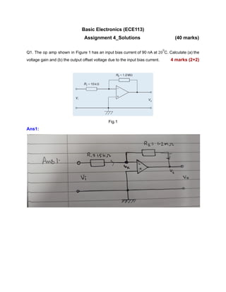
- 1. Basic Electronics (ECE113) Assignment 4_Solutions (40 marks) Q1. The op amp shown in Figure 1 has an input bias current of 90 nA at C. Calculate (a) the 20 0 voltage gain and (b) the output offset voltage due to the input bias current. 4 marks (2+2) Fig.1 Ans1:
- 2. Q2. Determine (a) the value of the feedback resistor and (b) the frequency for an inverting amplifier to have a voltage gain of 45 dB, a closed-loop bandwidth of 10 kHz and an input resistance of 20 k. 4 marks (2+2) Ans2:
- 4. Q3. A steady voltage of −1.25 V is applied to an op amp integrator having component values of R=125 k and C =4.0μF. Calculate the value of the output voltage 120 ms after applying the input, assuming that the initial capacitor charge is zero. 4 marks Ans3:
- 5. Q4. In the differential amplifier shown in Fig. 4, determine the output voltage, Vo, if: (a) V1 =4 mV and V2 =0, (b) V1=40 mV and V2 =30 mV, (c) V1 =25 mV and V2 =40 mV. 3 marks (2+2+1) Fig.4 Ans4:
- 6. Q5. Derive the transfer function for the circuit shown in figure 5. Find the high frequency gain and the cutoff frequency (2 marks upto here). Design the circuit to obtain a high frequency gain of 20 dB, 3 dB cutoff frequency of 10 kHz and a high frequency input resistance of 1 K (2 marks upto here). What is the unity gain bandwidth of this amplifier? (1 marks upto here) Fig.5 5 marks (2+2+1) Ans5:
- 9. Q6. Derive an expression for the input resistance of the inverting amplifier of Figure 6 taking into account the finite open-loop `gain, A of the op-amp. 4 marks Fig.6 Ans6:
- 12. Q7. The switching circuit of Fig. 7 contains two silicon diodes. For switch S closed, estimate 𝐼𝑎 and for 𝐼𝑏 𝑉𝑎 = − 1, − 0. 1, + 1 & + 2 𝑉. (a) For switch S open, estimate and for 4 marks (2+2) 𝐼𝑎 𝐼𝑏 𝑉𝑎 = + 1 𝑉. Fig.7 Ans7:
- 15. Q8. A common application of silicon diodes is shown in Fig.8. Predict as a function of 𝐼2 𝑉1 Fig. 8 4 marks Ans8:
- 16. Q9. Consider the silicon diode circuits of Fig. 9 (a & b). Let 𝑉1 = 5𝑉, 𝑉2 = 0, 𝑉𝑐𝑐 = 6𝑉. Determine for both (a) & (b). 𝑉𝑜 Fig.9 4 marks (2+2) Ans9:
- 17. ● Q10. Zener diode shown in Figure 10 has a breakdown voltage ( ) of 6 V. It is used in a 𝑉𝑍 voltage regulator circuit to regulate the output voltage. If = 2.5 kΩ, find the output voltage, 𝑅𝐿 power dissipation across the Zener diode and the load resistance . If the value of is 𝑅𝐿 𝑅𝐿 changed to 4 kΩ, find the power dissipation across the Zener diode. 4 marks (3+1)
- 18. Fig.10 Ans10