SlideShare a Scribd company logo
1 of 20
Download to read offline
INSTRUCTIONS:
1. Read the questions properly.
2. Provide the answer on the same sheet, student can use separate sheet where
necessary
PRACTICAL ASSIGNMENT – 01
NAME
CLASS
DATE
LEVEL Skill Proficiency Certificate
QUALIFICATION NO 3529-12
PRACTICAL
COMPETENCY
Electronic Applications
- Rectifier Filter
- Shunt Regulator Circuit
- Series Regulator Circuit
TASK 2.7 a Construct a voltage stabiliser using a series resistor and a
zener diode.
b Connect a load resistor to the circuit.
c Connect a d.c. supply to the input and measure the voltage
across the load resistor for changes in d.c. supply voltages.
d Record input and output voltages.
2.8 Convert circuit diagrams into layout diagrams.
2.9 Sketch a circuit diagram (to include d.c. power supply
connections) of a common emitter amplifier utilising an NPN
transistor, a base bias resistor and a collector load resistor.
TOTAL MARKS 100 MARKS OBTAINED
%AGE RESULT (PASS/FAIL)
INSTRUCTOR/ASSESSOR
NAME
INSTRUCTOR/ASSESSOR
SIGNATURE
Task:
A (i) Half Wave Rectifier
Figure 1: Half Wave Rectifier
Figure 2: Graph for Input & Output
A (ii) Full Wave Bridge Rectifier
Figure 3: Full Wave Bridge Rectifier
Figure 4: Graph for Output
B (i) Capacitor Filter Circuit
Figure 5: Capacitor Filter Circuit
Figure 6 : Graph for Output (RL is not Connected)
Figure 7 : Graph for Output (RL = 1k)
Figure 8 : Graph for Output (RL= 150)
C (i) Shunt Regulator
Input voltage keep constant
Figure 9 : Shunt Regulator
Figure 10 : Output Graph (RL)
VI (DC) RL IL VL VR IL IR
5V
1mA
5mA
10mA
10V
1mA
5mA
10mA
12V
1mA
5mA
10mA
Table 1 : Output Calculation Table
COMPETENCY CHECKLIST
COMPETENCY LEVEL:
C = COMPETENT, NC= NOT COMPETENT, PC = PARTIALLY COMPETENT
NO TASK MAXIMUM
MARKS
MARKS
OBTAINED
COMPENTENCY
LEVEL
ASSESSOR
COMMENTS
TASK A(i)
1 Circuit Wiring 5
2 Accurate Graph
Drawn
10
TASK A(ii)
1 Circuit Wiring 5
2 Accurate Graph
Drawn
10
TASK B(i)
1 Circuit Wiring 5
2 Graph for Output
(RL is not
Connected)
10
3 Graph for Output
(RL = 1k)
10
4 Graph for Output
(RL = 150)
10
TASK C(i)
1 Circuit Wiring 5
2 Graph for Output
(RL)
10
3 Output
Measurement for
Table 1
20
Guideline:
C = 60% and Above
PC = 40-59%
NC = 0-39%
PRACTICAL ASSIGNMENT – 02
NAME
CLASS
DATE
LEVEL Skill Proficiency Certificate
QUALIFICATION NO 3529-12
PRACTICAL
COMPETENCY
Electronic Applications
TASK 2.9 Sketch a circuit diagram (to include d.c. power supply connections) of a
common emitter amplifier utilizing an NPN transistor, a base bias resistor
and a collector load resistor.
2.10
a. With reference to 2.9, construct a simple common emitter amplifier
circuit.
b. Test the collector voltage).
c. Transfer the amplifier circuit to strip board (veroboard).
2.11
a. Connect a low-level signal (sine wave) from the function generator
to the input of the amplifier (as in 2.10).
b. Connect a dual-beam scope to monitor the input and output
waveforms and compare the input and output voltages.
2.12 Determine the voltage gain of the common emitter amplifier.
2.13
a. Observe the effect on voltage gain of varying the input frequency to
an amplifier.
b. Record voltage gain at each frequency.
Plot a frequency response curve for the amplifier from results obtained.
TOTAL MARKS 40 MARKS OBTAINED
%AGE RESULT (PASS/FAIL)
INSTRUCTOR/ASSESSOR
NAME
INSTRUCTOR/ASSESSOR
SIGNATURE
INSTRUCTIONS:
1. Read the questions properly.
2. Provide the answer on the same sheet, student can use separate sheet where
necessary.
Task 1
(A) Construct the Voltage Stabilizer Circuit from the Circuit Diagram below:
Figure 1 : Single Stage Amplifer
Set Actual Measure Actual Measure
Account
R5 Ve(V) Vbe(V) Vce(V) Rt(KΩ) Ib(µA) Ic(mA)
100%
60%
40%
Table 1: Record Table (Single Stage Amplifier)
(B) Basic Dynamics of Single-Stage Amplifier :
i. Use Function Generator with following configuration:
F=1 kHz
Amplitude=500mV
ii. Increase the input frequency gradually and fill in the table below for different values
of frequency.
Actual Test Actual Test Calculated
Vi(mV) Vo(mV) Av Av
Table 2 : Voltage Gain Calculation
(C) Effect of Load to Magnification:
Keep the Vi = 5mV unchanged, connect to load RL, change RC value and fill in the table
below:
Given Parameter Actual Measure Actual
Measure
Account
Estimated
Rc (R8) R-L (R9) Vi (mV) Vo (V) Av Av
2k 5k1
2k 2k2
5k1 5k1
5k1 2k2
COMPETENCY CHECKLIST
COMPETENCY LEVEL:
C = COMPETENT, NC= NOT COMPETENT, PC = PARTIALLY COMPETENT
NO TASK MAXIMUM
MARKS
MARKS
OBTAINED
COMPENTENCY
LEVEL
ASSESSOR
COMMENTS
1 1A - Circuit
Wiring
8
2 1A - Circuit
Operational
8
3 1A - Table 1
Values Recorded
8
4 1B – Table 2
Values recorded
8
5 1C – Table 3
Values Recorded
8
Guideline:
C = 60% and Above
PC = 40-59%
NC = 0-39%
1. Read the questions properly.
2. Provide the answer on the same sheet, student can use separate sheet where
necessary.
PRACTICAL ASSIGNMENT – 03
NAME
CLASS
DATE
LEVEL Skill Proficiency Certificate
QUALIFICATION NO 3529-12
PRACTICAL
COMPETENCY
Electronic Applications
- Transistor Switch
- Light Operated Relay
TASK 2.14 Construct and test the operation of the following circuits:
a. Series Voltage Regulator
b. Integrated Voltage Regulator
TOTAL MARKS 50 MARKS OBTAINED
%AGE RESULT (PASS/FAIL)
INSTRUCTOR/ASSESSOR
NAME
INSTRUCTOR/ASSESSOR
SIGNATURE
Task A (i): Transistor Voltage Regulator
Figure 1 : Series Voltage Regulator
Static Measurement
Q 1: What is the role of R2 resistor and LED in the above circuit?
Q 2: Draw data table?
Q 3:
a. Adjust +5V ~ +12V power to 9V, connect to Vi terminal, then adjust the
potentiometer RP, Let the Vo = 6V and measure Q point of each transistor.
b. Draw Q point of each transistor from above circuit:
COMPETENCY CHECKLIST
COMPETENCY LEVEL:
C = COMPETENT, NC= NOT COMPETENT, PC = PARTIALLY COMPETENT
NO TASK
MAXIMUM
MARKS
MARKS
OBTAINED
COMPENTENCY
LEVEL
ASSESSOR
COMMENTS
Q 1
1
Components
Identified
5
2 Circuit Wired 5
3
Circuit
Operation
10
4
Table Data
Recorded
10
Q 2
1
Components
Identified
5
2 Circuit Wiring 5
3 Q point graphs 10
Guideline:
C = 60% and Above
PC = 40-59%
NC = 0-39%
1. Read the questions properly.
2. Provide the answer on the same sheet, student can use separate sheet where
necessary.
PRACTICAL ASSIGNMENT – 04
NAME
CLASS
DATE
LEVEL Skill Proficiency Certificate
QUALIFICATION NO 3529-12
PRACTICAL
COMPETENCY
Electronic Applications
- Transistor Switch
- Light Operated Relay
TASK 2.17
a. Construct and test a simple timing circuit using a 555 timer
and other components.
b. Use an LED to indicate ON time.
2.18 Construct and test a timing circuit using a 555 timer which will
operate a 12V relay.
2.19
a. Construct an oscillator circuit using a 555 timer and other
components.
b. Observe and record the output waveform using an
oscilloscope.
TOTAL MARKS 50 MARKS OBTAINED
%AGE RESULT (PASS/FAIL)
INSTRUCTOR/ASSESSOR
NAME
INSTRUCTOR/ASSESSOR
SIGNATURE
TASK 1:
555 TIMER TEST WIRING DIAGRAM
Figure 1: 555 Timer Test Diagram
Layout:
Fig: Graph for TR and Q
COMPETENCY CHECKLIST
COMPETENCY LEVEL:
C = COMPETENT, NC= NOT COMPETENT, PC = PARTIALLY COMPETENT
NO TASK
MAXIMUM
MARKS
MARKS
OBTAINED
COMPENTENCY
LEVEL
ASSESSOR
COMMENTS
TASK 1
1
Components
Identified
5
2
Circuit
Assembled
5
3
Circuit
Operation
10
4
Layout is
drawn
10
TASK 2
1
U1(TR) and
U1(Q) Graph
Drawn
10
Guideline:
C = 60% and Above
PC = 40-59%
NC = 0-39%

More Related Content

What's hot

EE454_Power Flow Programming
EE454_Power Flow ProgrammingEE454_Power Flow Programming
EE454_Power Flow Programmingki hei chan
 
Dc analysis of four resistor biasing circuit
Dc analysis of four resistor biasing circuitDc analysis of four resistor biasing circuit
Dc analysis of four resistor biasing circuitMahoneyKadir
 
L08 power amplifier (class a)
L08 power amplifier (class a)L08 power amplifier (class a)
L08 power amplifier (class a)hasanen22
 
Differential amplifiers (content)
Differential amplifiers (content)Differential amplifiers (content)
Differential amplifiers (content)MahoneyKadir
 
EE456_NWPUD Transmission Reinforcement Planning
EE456_NWPUD Transmission Reinforcement PlanningEE456_NWPUD Transmission Reinforcement Planning
EE456_NWPUD Transmission Reinforcement Planningki hei chan
 
Smart Power Amplifier
Smart Power AmplifierSmart Power Amplifier
Smart Power AmplifierMagdi Mohamed
 
36.voltage divider bias
36.voltage divider bias36.voltage divider bias
36.voltage divider biasDoCircuits
 
Ac analysis of bjt and mosfet voltage followers
Ac analysis of bjt and mosfet voltage followersAc analysis of bjt and mosfet voltage followers
Ac analysis of bjt and mosfet voltage followersMahoneyKadir
 
Design Basics on Power Amplifiers
Design Basics on Power Amplifiers Design Basics on Power Amplifiers
Design Basics on Power Amplifiers ls234
 
Ac analysis of bjt and mosfet non-inverting amplifiers
Ac analysis of bjt and mosfet non-inverting amplifiersAc analysis of bjt and mosfet non-inverting amplifiers
Ac analysis of bjt and mosfet non-inverting amplifiersMahoneyKadir
 
ANALOG TO DIGITAL CONVERTERS
ANALOG TO DIGITAL CONVERTERSANALOG TO DIGITAL CONVERTERS
ANALOG TO DIGITAL CONVERTERSHarsha Raju
 
Regions of operation of bjt and mosfet
Regions of operation of bjt and mosfetRegions of operation of bjt and mosfet
Regions of operation of bjt and mosfetMahoneyKadir
 
Solved MSBTE Sample Paper Basic Electonics (EJ2I)
Solved MSBTE Sample Paper Basic Electonics (EJ2I)Solved MSBTE Sample Paper Basic Electonics (EJ2I)
Solved MSBTE Sample Paper Basic Electonics (EJ2I)Mangesh Gade
 
Ac analysis of bjt and mosfet inverting amplifiers
Ac analysis of bjt and mosfet inverting amplifiersAc analysis of bjt and mosfet inverting amplifiers
Ac analysis of bjt and mosfet inverting amplifiersMahoneyKadir
 

What's hot (20)

EE454_Power Flow Programming
EE454_Power Flow ProgrammingEE454_Power Flow Programming
EE454_Power Flow Programming
 
Adc2
Adc2Adc2
Adc2
 
Dc analysis of four resistor biasing circuit
Dc analysis of four resistor biasing circuitDc analysis of four resistor biasing circuit
Dc analysis of four resistor biasing circuit
 
L08 power amplifier (class a)
L08 power amplifier (class a)L08 power amplifier (class a)
L08 power amplifier (class a)
 
Differential amplifiers (content)
Differential amplifiers (content)Differential amplifiers (content)
Differential amplifiers (content)
 
EE456_NWPUD Transmission Reinforcement Planning
EE456_NWPUD Transmission Reinforcement PlanningEE456_NWPUD Transmission Reinforcement Planning
EE456_NWPUD Transmission Reinforcement Planning
 
Smart Power Amplifier
Smart Power AmplifierSmart Power Amplifier
Smart Power Amplifier
 
Chapter 1 ac analysis SKEE 2253
Chapter 1 ac analysis SKEE 2253Chapter 1 ac analysis SKEE 2253
Chapter 1 ac analysis SKEE 2253
 
36.voltage divider bias
36.voltage divider bias36.voltage divider bias
36.voltage divider bias
 
Ac analysis of bjt and mosfet voltage followers
Ac analysis of bjt and mosfet voltage followersAc analysis of bjt and mosfet voltage followers
Ac analysis of bjt and mosfet voltage followers
 
Design Basics on Power Amplifiers
Design Basics on Power Amplifiers Design Basics on Power Amplifiers
Design Basics on Power Amplifiers
 
Ac analysis of bjt and mosfet non-inverting amplifiers
Ac analysis of bjt and mosfet non-inverting amplifiersAc analysis of bjt and mosfet non-inverting amplifiers
Ac analysis of bjt and mosfet non-inverting amplifiers
 
ANALOG TO DIGITAL CONVERTERS
ANALOG TO DIGITAL CONVERTERSANALOG TO DIGITAL CONVERTERS
ANALOG TO DIGITAL CONVERTERS
 
Regions of operation of bjt and mosfet
Regions of operation of bjt and mosfetRegions of operation of bjt and mosfet
Regions of operation of bjt and mosfet
 
Solved MSBTE Sample Paper Basic Electonics (EJ2I)
Solved MSBTE Sample Paper Basic Electonics (EJ2I)Solved MSBTE Sample Paper Basic Electonics (EJ2I)
Solved MSBTE Sample Paper Basic Electonics (EJ2I)
 
Ac analysis of bjt and mosfet inverting amplifiers
Ac analysis of bjt and mosfet inverting amplifiersAc analysis of bjt and mosfet inverting amplifiers
Ac analysis of bjt and mosfet inverting amplifiers
 
Bjt transistors converted
Bjt transistors convertedBjt transistors converted
Bjt transistors converted
 
Pdc lab manualnew
Pdc lab manualnewPdc lab manualnew
Pdc lab manualnew
 
Power amplifier
Power amplifierPower amplifier
Power amplifier
 
Eca unit i.ppt
Eca unit i.pptEca unit i.ppt
Eca unit i.ppt
 

Similar to 3529-12 City&Guilds

SIGNAL SPECTRA EXPERIMENT 1 - FINALS (for PULA)
SIGNAL SPECTRA EXPERIMENT 1 - FINALS (for PULA)SIGNAL SPECTRA EXPERIMENT 1 - FINALS (for PULA)
SIGNAL SPECTRA EXPERIMENT 1 - FINALS (for PULA)Sarah Krystelle
 
SIGNAL SPECTRA EXPERIMENT 1 - FINALS (for AGDON)
SIGNAL SPECTRA EXPERIMENT 1 - FINALS (for AGDON)SIGNAL SPECTRA EXPERIMENT 1 - FINALS (for AGDON)
SIGNAL SPECTRA EXPERIMENT 1 - FINALS (for AGDON)Sarah Krystelle
 
SIGNAL SPECTRA EXPERIMENT 1 - FINALS (for ABDON)
SIGNAL SPECTRA EXPERIMENT 1 - FINALS (for ABDON)SIGNAL SPECTRA EXPERIMENT 1 - FINALS (for ABDON)
SIGNAL SPECTRA EXPERIMENT 1 - FINALS (for ABDON)Sarah Krystelle
 
SIGNAL SPECTRA EXPERIMENT 1 - FINALS (for CAUAN)
SIGNAL SPECTRA EXPERIMENT 1 - FINALS (for CAUAN)SIGNAL SPECTRA EXPERIMENT 1 - FINALS (for CAUAN)
SIGNAL SPECTRA EXPERIMENT 1 - FINALS (for CAUAN)Sarah Krystelle
 
Assignment 1 Description Marks out of Wtg() Due date .docx
Assignment 1  Description Marks out of Wtg() Due date .docxAssignment 1  Description Marks out of Wtg() Due date .docx
Assignment 1 Description Marks out of Wtg() Due date .docxfredharris32
 
Analog and Digital Electronics Lab Manual
Analog and Digital Electronics Lab ManualAnalog and Digital Electronics Lab Manual
Analog and Digital Electronics Lab ManualChirag Shetty
 
IRJET-Comparative Analysis of Rectangular and Square Column for Axial loading...
IRJET-Comparative Analysis of Rectangular and Square Column for Axial loading...IRJET-Comparative Analysis of Rectangular and Square Column for Axial loading...
IRJET-Comparative Analysis of Rectangular and Square Column for Axial loading...IRJET Journal
 
591321fghfryugfggffgghgghjhfgggggggggggggggg
591321fghfryugfggffgghgghjhfgggggggggggggggg591321fghfryugfggffgghgghjhfgggggggggggggggg
591321fghfryugfggffgghgghjhfggggggggggggggggankitch860
 
Analog Electronic Circuits - Module 5
Analog Electronic Circuits - Module 5Analog Electronic Circuits - Module 5
Analog Electronic Circuits - Module 5Aravinda Koithyar
 
Simulation and Experimental Verification of Single-Phase Pwm Boost -Rectifier...
Simulation and Experimental Verification of Single-Phase Pwm Boost -Rectifier...Simulation and Experimental Verification of Single-Phase Pwm Boost -Rectifier...
Simulation and Experimental Verification of Single-Phase Pwm Boost -Rectifier...IRJET Journal
 
WEEK 1 Assignment Power Amplifiers Week 1 Wor.docx
WEEK 1  Assignment  Power Amplifiers Week 1 Wor.docxWEEK 1  Assignment  Power Amplifiers Week 1 Wor.docx
WEEK 1 Assignment Power Amplifiers Week 1 Wor.docxcelenarouzie
 
Experiment no 2 setb118
Experiment no 2    setb118Experiment no 2    setb118
Experiment no 2 setb118Omkar Rane
 
EC8351-Electronic Circuits-I study material.pdf
EC8351-Electronic Circuits-I study material.pdfEC8351-Electronic Circuits-I study material.pdf
EC8351-Electronic Circuits-I study material.pdfRajaSekaran923497
 

Similar to 3529-12 City&Guilds (20)

SIGNAL SPECTRA EXPERIMENT 1 - FINALS (for PULA)
SIGNAL SPECTRA EXPERIMENT 1 - FINALS (for PULA)SIGNAL SPECTRA EXPERIMENT 1 - FINALS (for PULA)
SIGNAL SPECTRA EXPERIMENT 1 - FINALS (for PULA)
 
Exp f1 maycen
Exp f1 maycenExp f1 maycen
Exp f1 maycen
 
SIGNAL SPECTRA EXPERIMENT 1 - FINALS (for AGDON)
SIGNAL SPECTRA EXPERIMENT 1 - FINALS (for AGDON)SIGNAL SPECTRA EXPERIMENT 1 - FINALS (for AGDON)
SIGNAL SPECTRA EXPERIMENT 1 - FINALS (for AGDON)
 
SIGNAL SPECTRA EXPERIMENT 1 - FINALS (for ABDON)
SIGNAL SPECTRA EXPERIMENT 1 - FINALS (for ABDON)SIGNAL SPECTRA EXPERIMENT 1 - FINALS (for ABDON)
SIGNAL SPECTRA EXPERIMENT 1 - FINALS (for ABDON)
 
SIGNAL SPECTRA EXPERIMENT 1 - FINALS (for CAUAN)
SIGNAL SPECTRA EXPERIMENT 1 - FINALS (for CAUAN)SIGNAL SPECTRA EXPERIMENT 1 - FINALS (for CAUAN)
SIGNAL SPECTRA EXPERIMENT 1 - FINALS (for CAUAN)
 
Assignment 1 Description Marks out of Wtg() Due date .docx
Assignment 1  Description Marks out of Wtg() Due date .docxAssignment 1  Description Marks out of Wtg() Due date .docx
Assignment 1 Description Marks out of Wtg() Due date .docx
 
Analog and Digital Electronics Lab Manual
Analog and Digital Electronics Lab ManualAnalog and Digital Electronics Lab Manual
Analog and Digital Electronics Lab Manual
 
Ade manual final
Ade manual finalAde manual final
Ade manual final
 
IRJET-Comparative Analysis of Rectangular and Square Column for Axial loading...
IRJET-Comparative Analysis of Rectangular and Square Column for Axial loading...IRJET-Comparative Analysis of Rectangular and Square Column for Axial loading...
IRJET-Comparative Analysis of Rectangular and Square Column for Axial loading...
 
591321fghfryugfggffgghgghjhfgggggggggggggggg
591321fghfryugfggffgghgghjhfgggggggggggggggg591321fghfryugfggffgghgghjhfgggggggggggggggg
591321fghfryugfggffgghgghjhfgggggggggggggggg
 
ADC LAB MANUAL.docx
ADC LAB MANUAL.docxADC LAB MANUAL.docx
ADC LAB MANUAL.docx
 
Analog Electronic Circuits - Module 5
Analog Electronic Circuits - Module 5Analog Electronic Circuits - Module 5
Analog Electronic Circuits - Module 5
 
Simulation and Experimental Verification of Single-Phase Pwm Boost -Rectifier...
Simulation and Experimental Verification of Single-Phase Pwm Boost -Rectifier...Simulation and Experimental Verification of Single-Phase Pwm Boost -Rectifier...
Simulation and Experimental Verification of Single-Phase Pwm Boost -Rectifier...
 
WEEK 1 Assignment Power Amplifiers Week 1 Wor.docx
WEEK 1  Assignment  Power Amplifiers Week 1 Wor.docxWEEK 1  Assignment  Power Amplifiers Week 1 Wor.docx
WEEK 1 Assignment Power Amplifiers Week 1 Wor.docx
 
Experiment no 2 setb118
Experiment no 2    setb118Experiment no 2    setb118
Experiment no 2 setb118
 
A Commercial Low Cost, Highly Efficient UC3842 based High Brightness LED (HBL...
A Commercial Low Cost, Highly Efficient UC3842 based High Brightness LED (HBL...A Commercial Low Cost, Highly Efficient UC3842 based High Brightness LED (HBL...
A Commercial Low Cost, Highly Efficient UC3842 based High Brightness LED (HBL...
 
Power amplifier
Power amplifierPower amplifier
Power amplifier
 
D05432435
D05432435D05432435
D05432435
 
C04721623
C04721623C04721623
C04721623
 
EC8351-Electronic Circuits-I study material.pdf
EC8351-Electronic Circuits-I study material.pdfEC8351-Electronic Circuits-I study material.pdf
EC8351-Electronic Circuits-I study material.pdf
 

More from Hassan Khan

Proteus Circuits Design and Simulation - Examples and Projects
Proteus Circuits Design and Simulation - Examples and ProjectsProteus Circuits Design and Simulation - Examples and Projects
Proteus Circuits Design and Simulation - Examples and ProjectsHassan Khan
 
Timer Circuit (555 & 7447)
Timer Circuit (555 & 7447)Timer Circuit (555 & 7447)
Timer Circuit (555 & 7447)Hassan Khan
 
A+ B+B- A- Pneumatics and Electrical diagram
A+ B+B-  A- Pneumatics and Electrical diagramA+ B+B-  A- Pneumatics and Electrical diagram
A+ B+B- A- Pneumatics and Electrical diagramHassan Khan
 
Qasidah burdah shareef
Qasidah burdah shareefQasidah burdah shareef
Qasidah burdah shareefHassan Khan
 
FIELD SYSTEM by FANUC
FIELD SYSTEM by FANUCFIELD SYSTEM by FANUC
FIELD SYSTEM by FANUCHassan Khan
 
Light Control Switch
Light Control SwitchLight Control Switch
Light Control SwitchHassan Khan
 
Microsoft certified educator_study_guide
Microsoft certified educator_study_guideMicrosoft certified educator_study_guide
Microsoft certified educator_study_guideHassan Khan
 
Testing and other equipment (Electronics Beginner Level)
Testing and other equipment (Electronics Beginner Level)Testing and other equipment (Electronics Beginner Level)
Testing and other equipment (Electronics Beginner Level)Hassan Khan
 
Power supply 1.2 30 v (Beginners Level)
Power supply 1.2 30 v (Beginners Level)Power supply 1.2 30 v (Beginners Level)
Power supply 1.2 30 v (Beginners Level)Hassan Khan
 
Basic Electronics for Engineers (Tutorial)
Basic Electronics for Engineers (Tutorial)Basic Electronics for Engineers (Tutorial)
Basic Electronics for Engineers (Tutorial)Hassan Khan
 
PROTEUS - ARDUNIO PROGRAMMING FOR LCD
PROTEUS - ARDUNIO PROGRAMMING FOR LCDPROTEUS - ARDUNIO PROGRAMMING FOR LCD
PROTEUS - ARDUNIO PROGRAMMING FOR LCDHassan Khan
 
PROTEUS : ARDUINO PROJECT FOR LED N DC MOTOR
PROTEUS : ARDUINO PROJECT FOR LED N DC MOTORPROTEUS : ARDUINO PROJECT FOR LED N DC MOTOR
PROTEUS : ARDUINO PROJECT FOR LED N DC MOTORHassan Khan
 
Proteus Project : Arduino programming for LED
Proteus Project : Arduino programming for LEDProteus Project : Arduino programming for LED
Proteus Project : Arduino programming for LEDHassan Khan
 
555 74192 7447 .pdsprj
555 74192 7447 .pdsprj555 74192 7447 .pdsprj
555 74192 7447 .pdsprjHassan Khan
 
Certificate- City&Guilds L3
Certificate- City&Guilds L3Certificate- City&Guilds L3
Certificate- City&Guilds L3Hassan Khan
 

More from Hassan Khan (15)

Proteus Circuits Design and Simulation - Examples and Projects
Proteus Circuits Design and Simulation - Examples and ProjectsProteus Circuits Design and Simulation - Examples and Projects
Proteus Circuits Design and Simulation - Examples and Projects
 
Timer Circuit (555 & 7447)
Timer Circuit (555 & 7447)Timer Circuit (555 & 7447)
Timer Circuit (555 & 7447)
 
A+ B+B- A- Pneumatics and Electrical diagram
A+ B+B-  A- Pneumatics and Electrical diagramA+ B+B-  A- Pneumatics and Electrical diagram
A+ B+B- A- Pneumatics and Electrical diagram
 
Qasidah burdah shareef
Qasidah burdah shareefQasidah burdah shareef
Qasidah burdah shareef
 
FIELD SYSTEM by FANUC
FIELD SYSTEM by FANUCFIELD SYSTEM by FANUC
FIELD SYSTEM by FANUC
 
Light Control Switch
Light Control SwitchLight Control Switch
Light Control Switch
 
Microsoft certified educator_study_guide
Microsoft certified educator_study_guideMicrosoft certified educator_study_guide
Microsoft certified educator_study_guide
 
Testing and other equipment (Electronics Beginner Level)
Testing and other equipment (Electronics Beginner Level)Testing and other equipment (Electronics Beginner Level)
Testing and other equipment (Electronics Beginner Level)
 
Power supply 1.2 30 v (Beginners Level)
Power supply 1.2 30 v (Beginners Level)Power supply 1.2 30 v (Beginners Level)
Power supply 1.2 30 v (Beginners Level)
 
Basic Electronics for Engineers (Tutorial)
Basic Electronics for Engineers (Tutorial)Basic Electronics for Engineers (Tutorial)
Basic Electronics for Engineers (Tutorial)
 
PROTEUS - ARDUNIO PROGRAMMING FOR LCD
PROTEUS - ARDUNIO PROGRAMMING FOR LCDPROTEUS - ARDUNIO PROGRAMMING FOR LCD
PROTEUS - ARDUNIO PROGRAMMING FOR LCD
 
PROTEUS : ARDUINO PROJECT FOR LED N DC MOTOR
PROTEUS : ARDUINO PROJECT FOR LED N DC MOTORPROTEUS : ARDUINO PROJECT FOR LED N DC MOTOR
PROTEUS : ARDUINO PROJECT FOR LED N DC MOTOR
 
Proteus Project : Arduino programming for LED
Proteus Project : Arduino programming for LEDProteus Project : Arduino programming for LED
Proteus Project : Arduino programming for LED
 
555 74192 7447 .pdsprj
555 74192 7447 .pdsprj555 74192 7447 .pdsprj
555 74192 7447 .pdsprj
 
Certificate- City&Guilds L3
Certificate- City&Guilds L3Certificate- City&Guilds L3
Certificate- City&Guilds L3
 

Recently uploaded

Accessible design: Minimum effort, maximum impact
Accessible design: Minimum effort, maximum impactAccessible design: Minimum effort, maximum impact
Accessible design: Minimum effort, maximum impactdawncurless
 
Arihant handbook biology for class 11 .pdf
Arihant handbook biology for class 11 .pdfArihant handbook biology for class 11 .pdf
Arihant handbook biology for class 11 .pdfchloefrazer622
 
Measures of Dispersion and Variability: Range, QD, AD and SD
Measures of Dispersion and Variability: Range, QD, AD and SDMeasures of Dispersion and Variability: Range, QD, AD and SD
Measures of Dispersion and Variability: Range, QD, AD and SDThiyagu K
 
Nutritional Needs Presentation - HLTH 104
Nutritional Needs Presentation - HLTH 104Nutritional Needs Presentation - HLTH 104
Nutritional Needs Presentation - HLTH 104misteraugie
 
Q4-W6-Restating Informational Text Grade 3
Q4-W6-Restating Informational Text Grade 3Q4-W6-Restating Informational Text Grade 3
Q4-W6-Restating Informational Text Grade 3JemimahLaneBuaron
 
Activity 01 - Artificial Culture (1).pdf
Activity 01 - Artificial Culture (1).pdfActivity 01 - Artificial Culture (1).pdf
Activity 01 - Artificial Culture (1).pdfciinovamais
 
Disha NEET Physics Guide for classes 11 and 12.pdf
Disha NEET Physics Guide for classes 11 and 12.pdfDisha NEET Physics Guide for classes 11 and 12.pdf
Disha NEET Physics Guide for classes 11 and 12.pdfchloefrazer622
 
social pharmacy d-pharm 1st year by Pragati K. Mahajan
social pharmacy d-pharm 1st year by Pragati K. Mahajansocial pharmacy d-pharm 1st year by Pragati K. Mahajan
social pharmacy d-pharm 1st year by Pragati K. Mahajanpragatimahajan3
 
JAPAN: ORGANISATION OF PMDA, PHARMACEUTICAL LAWS & REGULATIONS, TYPES OF REGI...
JAPAN: ORGANISATION OF PMDA, PHARMACEUTICAL LAWS & REGULATIONS, TYPES OF REGI...JAPAN: ORGANISATION OF PMDA, PHARMACEUTICAL LAWS & REGULATIONS, TYPES OF REGI...
JAPAN: ORGANISATION OF PMDA, PHARMACEUTICAL LAWS & REGULATIONS, TYPES OF REGI...anjaliyadav012327
 
1029 - Danh muc Sach Giao Khoa 10 . pdf
1029 -  Danh muc Sach Giao Khoa 10 . pdf1029 -  Danh muc Sach Giao Khoa 10 . pdf
1029 - Danh muc Sach Giao Khoa 10 . pdfQucHHunhnh
 
Interactive Powerpoint_How to Master effective communication
Interactive Powerpoint_How to Master effective communicationInteractive Powerpoint_How to Master effective communication
Interactive Powerpoint_How to Master effective communicationnomboosow
 
The byproduct of sericulture in different industries.pptx
The byproduct of sericulture in different industries.pptxThe byproduct of sericulture in different industries.pptx
The byproduct of sericulture in different industries.pptxShobhayan Kirtania
 
Mastering the Unannounced Regulatory Inspection
Mastering the Unannounced Regulatory InspectionMastering the Unannounced Regulatory Inspection
Mastering the Unannounced Regulatory InspectionSafetyChain Software
 
BASLIQ CURRENT LOOKBOOK LOOKBOOK(1) (1).pdf
BASLIQ CURRENT LOOKBOOK  LOOKBOOK(1) (1).pdfBASLIQ CURRENT LOOKBOOK  LOOKBOOK(1) (1).pdf
BASLIQ CURRENT LOOKBOOK LOOKBOOK(1) (1).pdfSoniaTolstoy
 
Paris 2024 Olympic Geographies - an activity
Paris 2024 Olympic Geographies - an activityParis 2024 Olympic Geographies - an activity
Paris 2024 Olympic Geographies - an activityGeoBlogs
 
Sports & Fitness Value Added Course FY..
Sports & Fitness Value Added Course FY..Sports & Fitness Value Added Course FY..
Sports & Fitness Value Added Course FY..Disha Kariya
 
Beyond the EU: DORA and NIS 2 Directive's Global Impact
Beyond the EU: DORA and NIS 2 Directive's Global ImpactBeyond the EU: DORA and NIS 2 Directive's Global Impact
Beyond the EU: DORA and NIS 2 Directive's Global ImpactPECB
 
Introduction to Nonprofit Accounting: The Basics
Introduction to Nonprofit Accounting: The BasicsIntroduction to Nonprofit Accounting: The Basics
Introduction to Nonprofit Accounting: The BasicsTechSoup
 

Recently uploaded (20)

Accessible design: Minimum effort, maximum impact
Accessible design: Minimum effort, maximum impactAccessible design: Minimum effort, maximum impact
Accessible design: Minimum effort, maximum impact
 
Arihant handbook biology for class 11 .pdf
Arihant handbook biology for class 11 .pdfArihant handbook biology for class 11 .pdf
Arihant handbook biology for class 11 .pdf
 
Measures of Dispersion and Variability: Range, QD, AD and SD
Measures of Dispersion and Variability: Range, QD, AD and SDMeasures of Dispersion and Variability: Range, QD, AD and SD
Measures of Dispersion and Variability: Range, QD, AD and SD
 
Nutritional Needs Presentation - HLTH 104
Nutritional Needs Presentation - HLTH 104Nutritional Needs Presentation - HLTH 104
Nutritional Needs Presentation - HLTH 104
 
Q4-W6-Restating Informational Text Grade 3
Q4-W6-Restating Informational Text Grade 3Q4-W6-Restating Informational Text Grade 3
Q4-W6-Restating Informational Text Grade 3
 
Activity 01 - Artificial Culture (1).pdf
Activity 01 - Artificial Culture (1).pdfActivity 01 - Artificial Culture (1).pdf
Activity 01 - Artificial Culture (1).pdf
 
Código Creativo y Arte de Software | Unidad 1
Código Creativo y Arte de Software | Unidad 1Código Creativo y Arte de Software | Unidad 1
Código Creativo y Arte de Software | Unidad 1
 
Disha NEET Physics Guide for classes 11 and 12.pdf
Disha NEET Physics Guide for classes 11 and 12.pdfDisha NEET Physics Guide for classes 11 and 12.pdf
Disha NEET Physics Guide for classes 11 and 12.pdf
 
social pharmacy d-pharm 1st year by Pragati K. Mahajan
social pharmacy d-pharm 1st year by Pragati K. Mahajansocial pharmacy d-pharm 1st year by Pragati K. Mahajan
social pharmacy d-pharm 1st year by Pragati K. Mahajan
 
JAPAN: ORGANISATION OF PMDA, PHARMACEUTICAL LAWS & REGULATIONS, TYPES OF REGI...
JAPAN: ORGANISATION OF PMDA, PHARMACEUTICAL LAWS & REGULATIONS, TYPES OF REGI...JAPAN: ORGANISATION OF PMDA, PHARMACEUTICAL LAWS & REGULATIONS, TYPES OF REGI...
JAPAN: ORGANISATION OF PMDA, PHARMACEUTICAL LAWS & REGULATIONS, TYPES OF REGI...
 
1029 - Danh muc Sach Giao Khoa 10 . pdf
1029 -  Danh muc Sach Giao Khoa 10 . pdf1029 -  Danh muc Sach Giao Khoa 10 . pdf
1029 - Danh muc Sach Giao Khoa 10 . pdf
 
Interactive Powerpoint_How to Master effective communication
Interactive Powerpoint_How to Master effective communicationInteractive Powerpoint_How to Master effective communication
Interactive Powerpoint_How to Master effective communication
 
The byproduct of sericulture in different industries.pptx
The byproduct of sericulture in different industries.pptxThe byproduct of sericulture in different industries.pptx
The byproduct of sericulture in different industries.pptx
 
Mastering the Unannounced Regulatory Inspection
Mastering the Unannounced Regulatory InspectionMastering the Unannounced Regulatory Inspection
Mastering the Unannounced Regulatory Inspection
 
BASLIQ CURRENT LOOKBOOK LOOKBOOK(1) (1).pdf
BASLIQ CURRENT LOOKBOOK  LOOKBOOK(1) (1).pdfBASLIQ CURRENT LOOKBOOK  LOOKBOOK(1) (1).pdf
BASLIQ CURRENT LOOKBOOK LOOKBOOK(1) (1).pdf
 
Paris 2024 Olympic Geographies - an activity
Paris 2024 Olympic Geographies - an activityParis 2024 Olympic Geographies - an activity
Paris 2024 Olympic Geographies - an activity
 
Sports & Fitness Value Added Course FY..
Sports & Fitness Value Added Course FY..Sports & Fitness Value Added Course FY..
Sports & Fitness Value Added Course FY..
 
Beyond the EU: DORA and NIS 2 Directive's Global Impact
Beyond the EU: DORA and NIS 2 Directive's Global ImpactBeyond the EU: DORA and NIS 2 Directive's Global Impact
Beyond the EU: DORA and NIS 2 Directive's Global Impact
 
Introduction to Nonprofit Accounting: The Basics
Introduction to Nonprofit Accounting: The BasicsIntroduction to Nonprofit Accounting: The Basics
Introduction to Nonprofit Accounting: The Basics
 
Advance Mobile Application Development class 07
Advance Mobile Application Development class 07Advance Mobile Application Development class 07
Advance Mobile Application Development class 07
 

3529-12 City&Guilds

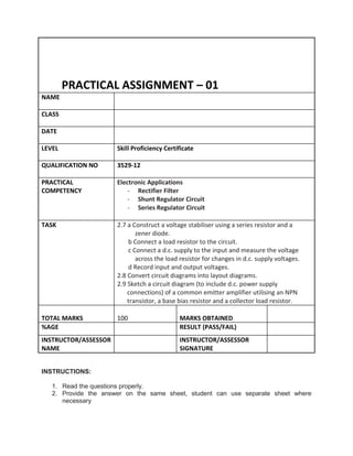
  • 1. INSTRUCTIONS: 1. Read the questions properly. 2. Provide the answer on the same sheet, student can use separate sheet where necessary PRACTICAL ASSIGNMENT – 01 NAME CLASS DATE LEVEL Skill Proficiency Certificate QUALIFICATION NO 3529-12 PRACTICAL COMPETENCY Electronic Applications - Rectifier Filter - Shunt Regulator Circuit - Series Regulator Circuit TASK 2.7 a Construct a voltage stabiliser using a series resistor and a zener diode. b Connect a load resistor to the circuit. c Connect a d.c. supply to the input and measure the voltage across the load resistor for changes in d.c. supply voltages. d Record input and output voltages. 2.8 Convert circuit diagrams into layout diagrams. 2.9 Sketch a circuit diagram (to include d.c. power supply connections) of a common emitter amplifier utilising an NPN transistor, a base bias resistor and a collector load resistor. TOTAL MARKS 100 MARKS OBTAINED %AGE RESULT (PASS/FAIL) INSTRUCTOR/ASSESSOR NAME INSTRUCTOR/ASSESSOR SIGNATURE
  • 2. Task: A (i) Half Wave Rectifier Figure 1: Half Wave Rectifier Figure 2: Graph for Input & Output
  • 3. A (ii) Full Wave Bridge Rectifier Figure 3: Full Wave Bridge Rectifier Figure 4: Graph for Output
  • 4. B (i) Capacitor Filter Circuit Figure 5: Capacitor Filter Circuit Figure 6 : Graph for Output (RL is not Connected)
  • 5. Figure 7 : Graph for Output (RL = 1k) Figure 8 : Graph for Output (RL= 150)
  • 6. C (i) Shunt Regulator Input voltage keep constant Figure 9 : Shunt Regulator Figure 10 : Output Graph (RL)
  • 7. VI (DC) RL IL VL VR IL IR 5V 1mA 5mA 10mA 10V 1mA 5mA 10mA 12V 1mA 5mA 10mA Table 1 : Output Calculation Table
  • 8. COMPETENCY CHECKLIST COMPETENCY LEVEL: C = COMPETENT, NC= NOT COMPETENT, PC = PARTIALLY COMPETENT NO TASK MAXIMUM MARKS MARKS OBTAINED COMPENTENCY LEVEL ASSESSOR COMMENTS TASK A(i) 1 Circuit Wiring 5 2 Accurate Graph Drawn 10 TASK A(ii) 1 Circuit Wiring 5 2 Accurate Graph Drawn 10 TASK B(i) 1 Circuit Wiring 5 2 Graph for Output (RL is not Connected) 10 3 Graph for Output (RL = 1k) 10 4 Graph for Output (RL = 150) 10 TASK C(i) 1 Circuit Wiring 5 2 Graph for Output (RL) 10 3 Output Measurement for Table 1 20 Guideline: C = 60% and Above PC = 40-59% NC = 0-39%
  • 9. PRACTICAL ASSIGNMENT – 02 NAME CLASS DATE LEVEL Skill Proficiency Certificate QUALIFICATION NO 3529-12 PRACTICAL COMPETENCY Electronic Applications TASK 2.9 Sketch a circuit diagram (to include d.c. power supply connections) of a common emitter amplifier utilizing an NPN transistor, a base bias resistor and a collector load resistor. 2.10 a. With reference to 2.9, construct a simple common emitter amplifier circuit. b. Test the collector voltage). c. Transfer the amplifier circuit to strip board (veroboard). 2.11 a. Connect a low-level signal (sine wave) from the function generator to the input of the amplifier (as in 2.10). b. Connect a dual-beam scope to monitor the input and output waveforms and compare the input and output voltages. 2.12 Determine the voltage gain of the common emitter amplifier. 2.13 a. Observe the effect on voltage gain of varying the input frequency to an amplifier. b. Record voltage gain at each frequency. Plot a frequency response curve for the amplifier from results obtained. TOTAL MARKS 40 MARKS OBTAINED %AGE RESULT (PASS/FAIL) INSTRUCTOR/ASSESSOR NAME INSTRUCTOR/ASSESSOR SIGNATURE
  • 10. INSTRUCTIONS: 1. Read the questions properly. 2. Provide the answer on the same sheet, student can use separate sheet where necessary. Task 1 (A) Construct the Voltage Stabilizer Circuit from the Circuit Diagram below: Figure 1 : Single Stage Amplifer Set Actual Measure Actual Measure Account R5 Ve(V) Vbe(V) Vce(V) Rt(KΩ) Ib(µA) Ic(mA) 100% 60% 40% Table 1: Record Table (Single Stage Amplifier)
  • 11. (B) Basic Dynamics of Single-Stage Amplifier : i. Use Function Generator with following configuration: F=1 kHz Amplitude=500mV ii. Increase the input frequency gradually and fill in the table below for different values of frequency. Actual Test Actual Test Calculated Vi(mV) Vo(mV) Av Av Table 2 : Voltage Gain Calculation (C) Effect of Load to Magnification: Keep the Vi = 5mV unchanged, connect to load RL, change RC value and fill in the table below: Given Parameter Actual Measure Actual Measure Account Estimated Rc (R8) R-L (R9) Vi (mV) Vo (V) Av Av 2k 5k1 2k 2k2 5k1 5k1 5k1 2k2
  • 12. COMPETENCY CHECKLIST COMPETENCY LEVEL: C = COMPETENT, NC= NOT COMPETENT, PC = PARTIALLY COMPETENT NO TASK MAXIMUM MARKS MARKS OBTAINED COMPENTENCY LEVEL ASSESSOR COMMENTS 1 1A - Circuit Wiring 8 2 1A - Circuit Operational 8 3 1A - Table 1 Values Recorded 8 4 1B – Table 2 Values recorded 8 5 1C – Table 3 Values Recorded 8 Guideline: C = 60% and Above PC = 40-59% NC = 0-39%
  • 13. 1. Read the questions properly. 2. Provide the answer on the same sheet, student can use separate sheet where necessary. PRACTICAL ASSIGNMENT – 03 NAME CLASS DATE LEVEL Skill Proficiency Certificate QUALIFICATION NO 3529-12 PRACTICAL COMPETENCY Electronic Applications - Transistor Switch - Light Operated Relay TASK 2.14 Construct and test the operation of the following circuits: a. Series Voltage Regulator b. Integrated Voltage Regulator TOTAL MARKS 50 MARKS OBTAINED %AGE RESULT (PASS/FAIL) INSTRUCTOR/ASSESSOR NAME INSTRUCTOR/ASSESSOR SIGNATURE
  • 14. Task A (i): Transistor Voltage Regulator Figure 1 : Series Voltage Regulator Static Measurement Q 1: What is the role of R2 resistor and LED in the above circuit?
  • 15. Q 2: Draw data table? Q 3: a. Adjust +5V ~ +12V power to 9V, connect to Vi terminal, then adjust the potentiometer RP, Let the Vo = 6V and measure Q point of each transistor. b. Draw Q point of each transistor from above circuit:
  • 16. COMPETENCY CHECKLIST COMPETENCY LEVEL: C = COMPETENT, NC= NOT COMPETENT, PC = PARTIALLY COMPETENT NO TASK MAXIMUM MARKS MARKS OBTAINED COMPENTENCY LEVEL ASSESSOR COMMENTS Q 1 1 Components Identified 5 2 Circuit Wired 5 3 Circuit Operation 10 4 Table Data Recorded 10 Q 2 1 Components Identified 5 2 Circuit Wiring 5 3 Q point graphs 10 Guideline: C = 60% and Above PC = 40-59% NC = 0-39%
  • 17. 1. Read the questions properly. 2. Provide the answer on the same sheet, student can use separate sheet where necessary. PRACTICAL ASSIGNMENT – 04 NAME CLASS DATE LEVEL Skill Proficiency Certificate QUALIFICATION NO 3529-12 PRACTICAL COMPETENCY Electronic Applications - Transistor Switch - Light Operated Relay TASK 2.17 a. Construct and test a simple timing circuit using a 555 timer and other components. b. Use an LED to indicate ON time. 2.18 Construct and test a timing circuit using a 555 timer which will operate a 12V relay. 2.19 a. Construct an oscillator circuit using a 555 timer and other components. b. Observe and record the output waveform using an oscilloscope. TOTAL MARKS 50 MARKS OBTAINED %AGE RESULT (PASS/FAIL) INSTRUCTOR/ASSESSOR NAME INSTRUCTOR/ASSESSOR SIGNATURE
  • 18. TASK 1: 555 TIMER TEST WIRING DIAGRAM Figure 1: 555 Timer Test Diagram Layout:
  • 19. Fig: Graph for TR and Q
  • 20. COMPETENCY CHECKLIST COMPETENCY LEVEL: C = COMPETENT, NC= NOT COMPETENT, PC = PARTIALLY COMPETENT NO TASK MAXIMUM MARKS MARKS OBTAINED COMPENTENCY LEVEL ASSESSOR COMMENTS TASK 1 1 Components Identified 5 2 Circuit Assembled 5 3 Circuit Operation 10 4 Layout is drawn 10 TASK 2 1 U1(TR) and U1(Q) Graph Drawn 10 Guideline: C = 60% and Above PC = 40-59% NC = 0-39%