This document proposes a novel structure to improve the common mode rejection ratio (CMRR) of circuits like current buffers and folded cascode amplifiers. The proposed structure uses only four transistors and a current source to deviate common mode signals without affecting differential mode signals. This improves the CMRR by at least 12dB while preserving the CMRR bandwidth, which is a novel technique. The structure was applied to both a current buffer and folded cascode amplifier based on simulation results, demonstrating its effectiveness in improving CMRR.
The Analysis of Dead Time on Switching Loss in High and Low Side MOSFETs of Z...IDES Editor
This work is about the analysis of dead time variation
on switching losses in a Zero Voltage Switching (ZVS)
synchronous buck converter (SBC) circuit. In high frequency
converter circuits, switching losses are commonly linked with
high and low side switches of SBC circuit. They are activated
externally by the gate driver circuit. The duty ratio, dead time
and resonant inductor are the parameters that affect the
efficiency of the circuit. These variables can be adjusted for
the optimization purposes. The study primarily focuses on
varying the settings of input pulses of the MOSFETs in the
resonant gate driver circuit which consequently affects the
performance of the ZVS synchronous buck converter circuit.
Using the predetermined inductor of 9 nH, the frequency is
maintained at 1 MHz for each cycle transition. The switching
loss graph is obtained and switching losses for both S1 and S2
are calculated and compared to the findings from previous
work. It has shown a decrease in losses by 13.8 % in S1. A dead
time of 15 ns has been determined to be optimized value in
the SBC design.
Optimized Hybrid Phase Disposition PWM Control Method for Multilevel InverterIDES Editor
This paper presents a new variation of hybrid
phase disposition pulse width modulation technique suitable
for cascaded multilevel inverter. A hybrid PDPWM is
developed based on low frequency PWM and high
frequency Sinusoidal PWM. An optimized sequential
switching scheme introduced in this proposed method to
equalize electro static and electro magnetic stress among the
power devices. It is confirmed that the proposed technique
offers significantly lower switching losses and switching
transitions. Furthermore, the proposed hybrid PDPWM
offers better harmonic performance compared to its
conventional PWM counterpart. Simulation results are
included in this paper in order to confirm the effectiveness
of the proposed technique.
FAST TRANSIENT RESPONSE LOW DROPOUT VOLTAGE REGULATORijseajournal
This paper presents the design of Low Drop-Out (LDO) voltage regulator has fast transient response and which exploits a few current else low quiescent current in the operational amplifier PMOS type. We use band-gap reference for eliminate the temperature dependence. The proposed LDO voltage regulator implemented in 0.18-μm CMOS technology, we use Folded cascode CMOS amplifiers high performance in the stability , provide fast transient response which explains a fast settling, the LDO itself should provide in the output regulator voltages at t equal 2ps with transient variation of the voltage less than 170mV. High accuracy in the DC response terms, the simulation results show that the accuracy of the output regulator voltages is 1.54±0.009V, and power consumption of 1.51 mW.
The Analysis of Dead Time on Switching Loss in High and Low Side MOSFETs of Z...IDES Editor
This work is about the analysis of dead time
variation on switching losses in a Zero Voltage Switching
(ZVS) synchronous buck converter (SBC) circuit. In high
frequency converter circuits, switching losses are
commonly linked with high and low side switches of SBC
circuit. They are activated externally by the gate driver
circuit. The duty ratio, dead time and resonant inductor
are the parameters that affect the efficiency of the circuit.
These variables can be adjusted for the optimization
purposes. The study primarily focuses on varying the
settings of input pulses of the MOSFETs in the resonant
gate driver circuit which consequently affects the
performance of the ZVS synchronous buck converter
circuit. Using the predetermined inductor of 9 nH, the
frequency is maintained at 1 MHz for each cycle
transition. The switching loss graph is obtained and
switching losses for both S1 and S2 are calculated and
compared to the findings from previous work. It has
shown a decrease in losses by 13.8 % in S1. A dead time of
15 ns has been determined to be optimized value in the
SBC design.
A New Soft-Switched Resonant DC-DC ConverterIDES Editor
This paper presents a new soft-switched resonant
dc-dc converter using a passive snubber circuit. The
proposed converter uses a new zero voltage and zero current
switching (ZVZCS) strategies to get ZVZCS function.
Besides operating at constant frequency, all semiconductor
devices operate at soft-switching without additional voltage
and current stresses. In order to validate the proposed
converter, computer simulations and experimental results
were conducted. The paper indicates the effective converter
operation region of the soft-switching action and its
efficiency improvement results on the basis of experimental
evaluations using laboratory prototype.
The Analysis of Dead Time on Switching Loss in High and Low Side MOSFETs of Z...IDES Editor
This work is about the analysis of dead time variation
on switching losses in a Zero Voltage Switching (ZVS)
synchronous buck converter (SBC) circuit. In high frequency
converter circuits, switching losses are commonly linked with
high and low side switches of SBC circuit. They are activated
externally by the gate driver circuit. The duty ratio, dead time
and resonant inductor are the parameters that affect the
efficiency of the circuit. These variables can be adjusted for
the optimization purposes. The study primarily focuses on
varying the settings of input pulses of the MOSFETs in the
resonant gate driver circuit which consequently affects the
performance of the ZVS synchronous buck converter circuit.
Using the predetermined inductor of 9 nH, the frequency is
maintained at 1 MHz for each cycle transition. The switching
loss graph is obtained and switching losses for both S1 and S2
are calculated and compared to the findings from previous
work. It has shown a decrease in losses by 13.8 % in S1. A dead
time of 15 ns has been determined to be optimized value in
the SBC design.
Optimized Hybrid Phase Disposition PWM Control Method for Multilevel InverterIDES Editor
This paper presents a new variation of hybrid
phase disposition pulse width modulation technique suitable
for cascaded multilevel inverter. A hybrid PDPWM is
developed based on low frequency PWM and high
frequency Sinusoidal PWM. An optimized sequential
switching scheme introduced in this proposed method to
equalize electro static and electro magnetic stress among the
power devices. It is confirmed that the proposed technique
offers significantly lower switching losses and switching
transitions. Furthermore, the proposed hybrid PDPWM
offers better harmonic performance compared to its
conventional PWM counterpart. Simulation results are
included in this paper in order to confirm the effectiveness
of the proposed technique.
FAST TRANSIENT RESPONSE LOW DROPOUT VOLTAGE REGULATORijseajournal
This paper presents the design of Low Drop-Out (LDO) voltage regulator has fast transient response and which exploits a few current else low quiescent current in the operational amplifier PMOS type. We use band-gap reference for eliminate the temperature dependence. The proposed LDO voltage regulator implemented in 0.18-μm CMOS technology, we use Folded cascode CMOS amplifiers high performance in the stability , provide fast transient response which explains a fast settling, the LDO itself should provide in the output regulator voltages at t equal 2ps with transient variation of the voltage less than 170mV. High accuracy in the DC response terms, the simulation results show that the accuracy of the output regulator voltages is 1.54±0.009V, and power consumption of 1.51 mW.
The Analysis of Dead Time on Switching Loss in High and Low Side MOSFETs of Z...IDES Editor
This work is about the analysis of dead time
variation on switching losses in a Zero Voltage Switching
(ZVS) synchronous buck converter (SBC) circuit. In high
frequency converter circuits, switching losses are
commonly linked with high and low side switches of SBC
circuit. They are activated externally by the gate driver
circuit. The duty ratio, dead time and resonant inductor
are the parameters that affect the efficiency of the circuit.
These variables can be adjusted for the optimization
purposes. The study primarily focuses on varying the
settings of input pulses of the MOSFETs in the resonant
gate driver circuit which consequently affects the
performance of the ZVS synchronous buck converter
circuit. Using the predetermined inductor of 9 nH, the
frequency is maintained at 1 MHz for each cycle
transition. The switching loss graph is obtained and
switching losses for both S1 and S2 are calculated and
compared to the findings from previous work. It has
shown a decrease in losses by 13.8 % in S1. A dead time of
15 ns has been determined to be optimized value in the
SBC design.
A New Soft-Switched Resonant DC-DC ConverterIDES Editor
This paper presents a new soft-switched resonant
dc-dc converter using a passive snubber circuit. The
proposed converter uses a new zero voltage and zero current
switching (ZVZCS) strategies to get ZVZCS function.
Besides operating at constant frequency, all semiconductor
devices operate at soft-switching without additional voltage
and current stresses. In order to validate the proposed
converter, computer simulations and experimental results
were conducted. The paper indicates the effective converter
operation region of the soft-switching action and its
efficiency improvement results on the basis of experimental
evaluations using laboratory prototype.
IJERA (International journal of Engineering Research and Applications) is International online, ... peer reviewed journal. For more detail or submit your article, please visit www.ijera.com
In this article, we proposed a Variable threshold MOSFET(VTMOS)approach which is realized from Dynamic Threshold MOSFET(DTMOS), suitable for sub-threshold digital circuit operation. Basically the principle of sub- threshold logics is operating MOSFET in sub-threshold region and using the leakage current in that region for switching action, there by drastically decreasing power .To reduce the power consumption of sub-threshold circuits further, a novel body biasing technique termed VTMOS is introduced .VTMOS approach is realized from DTMOS approach. Dynamic threshold MOS (DTMOS) circuits provide low leakage and high current drive, compared to CMOS circuits, operated at lower voltages.
The VTMOS is based on operating the MOS devices with an appropriate substrate bias which varies with gate voltage, by connecting a positive bias voltage between gate and substrate for NMOS and negative bias voltage between gate and substrate for PMOS. With VTMOS, there is a considerable reduction in operating current and power dissipation, while the remaining characteristics are almost the same as those of DTMOS. Results of our investigations show that VTMOS circuits improves the power up to 50% when compared to CMOS and DTMOS circuits, in sub- threshold region..
The performance analysis and comparison of VTMOS , DTMOS and CMOS is made and test results of Power dissipation, Propagation delay and Power delay product are presented to justify the superiority of VTMOS logic over conventional sub-threshold logics using Hspice Tool. . The dependency of these parameters on frequency of operation has also been investigated.
Electronics and Communication Engineering is the Branch of Engineering. Electronics and Communication Engineering field requires an understanding of core areas including Engineering Graphics, Computer Programming,Electronics Devices and Circuits-I, Network Analysis, Signals and Systems, Communication Systems, Electromagnetics Engineering, Digital Signal Processing, Embedded Systems, Microprocessor and Computer Architecture. Ekeeda offers Online Mechanical Engineering Courses for all the Subjects as per the Syllabus. Visit : https://ekeeda.com/streamdetails/stream/Electronics-and-Communication-Engineering
Common Mode Voltage Control in Three Level Diode Clamped InverterIJERA Editor
This paper presents simple sinusoidal PWM technique to reduced common mode voltage (CMV) at output terminal of the inverter. Multilevel inverter (MLI) is more suitable in high & medium power application, CMV is produced at the time of operation in output terminal of inverter. In this paper, an approach to reduced CMV at output terminal of MLI by using SPWM technique in three level diode clamped inverter (DCMLI) is proposed. A good transaction between the quality of the output voltage & the magnitude of CMV is achieved in this paper. The paper presents phase opposition & phase opposition disposition SPWM technique to reduced CMV in DCMLI. Simulation & experimental result presented to confirm the effectiveness of the proposed technique to control CMV.
An operational amplifier with recycling folded cascode topology and adaptive ...VLSICS Design
This paper presents a highly adaptive operational amplifier with high gain, high bandwidth, high speed
and low power consumption. By adopting the recycling folded cascode topology along with an adaptivebiasing
circuit, this design achieves high performance in terms of gain-bandwidth product (GBW) and slew
rate (SR). This single stage op-amp has been designed in 0.18μm technology with a power supply of 1.8V
and a 5pF load. The simulation results show that the amplifier achieved a GBW of 335.5MHz, Unity Gain
Bandwidth of 247.1MHz and a slew rate of 92.8V/μs.
IJERA (International journal of Engineering Research and Applications) is International online, ... peer reviewed journal. For more detail or submit your article, please visit www.ijera.com
Open Loop Control Of Series Parallel Resonant ConverterIDES Editor
Resonant converters are desirable for power
conversion due to their comparatively smaller size and
lower power losses resulting from high-frequency
operation and inherent soft switching. Among all the
topologies of the resonant converters, the series–parallel
resonant converter (SPRC) is known to have the
combined merits of the series resonant converter and
parallel resonant converter. The converter can regulate
the output voltage at a constant switching frequency even
for a change in load resistance from full load resistance to
infinity while maintaining good part load efficiency. The
purpose of this project is to design a closed loop
controller for the phase-controlled series parallel
resonant converter (PC SPRC). The open loop analysis
and closed loop control has been provided in this paper.
IJERA (International journal of Engineering Research and Applications) is International online, ... peer reviewed journal. For more detail or submit your article, please visit www.ijera.com
In this article, we proposed a Variable threshold MOSFET(VTMOS)approach which is realized from Dynamic Threshold MOSFET(DTMOS), suitable for sub-threshold digital circuit operation. Basically the principle of sub- threshold logics is operating MOSFET in sub-threshold region and using the leakage current in that region for switching action, there by drastically decreasing power .To reduce the power consumption of sub-threshold circuits further, a novel body biasing technique termed VTMOS is introduced .VTMOS approach is realized from DTMOS approach. Dynamic threshold MOS (DTMOS) circuits provide low leakage and high current drive, compared to CMOS circuits, operated at lower voltages.
The VTMOS is based on operating the MOS devices with an appropriate substrate bias which varies with gate voltage, by connecting a positive bias voltage between gate and substrate for NMOS and negative bias voltage between gate and substrate for PMOS. With VTMOS, there is a considerable reduction in operating current and power dissipation, while the remaining characteristics are almost the same as those of DTMOS. Results of our investigations show that VTMOS circuits improves the power up to 50% when compared to CMOS and DTMOS circuits, in sub- threshold region..
The performance analysis and comparison of VTMOS , DTMOS and CMOS is made and test results of Power dissipation, Propagation delay and Power delay product are presented to justify the superiority of VTMOS logic over conventional sub-threshold logics using Hspice Tool. . The dependency of these parameters on frequency of operation has also been investigated.
Electronics and Communication Engineering is the Branch of Engineering. Electronics and Communication Engineering field requires an understanding of core areas including Engineering Graphics, Computer Programming,Electronics Devices and Circuits-I, Network Analysis, Signals and Systems, Communication Systems, Electromagnetics Engineering, Digital Signal Processing, Embedded Systems, Microprocessor and Computer Architecture. Ekeeda offers Online Mechanical Engineering Courses for all the Subjects as per the Syllabus. Visit : https://ekeeda.com/streamdetails/stream/Electronics-and-Communication-Engineering
Common Mode Voltage Control in Three Level Diode Clamped InverterIJERA Editor
This paper presents simple sinusoidal PWM technique to reduced common mode voltage (CMV) at output terminal of the inverter. Multilevel inverter (MLI) is more suitable in high & medium power application, CMV is produced at the time of operation in output terminal of inverter. In this paper, an approach to reduced CMV at output terminal of MLI by using SPWM technique in three level diode clamped inverter (DCMLI) is proposed. A good transaction between the quality of the output voltage & the magnitude of CMV is achieved in this paper. The paper presents phase opposition & phase opposition disposition SPWM technique to reduced CMV in DCMLI. Simulation & experimental result presented to confirm the effectiveness of the proposed technique to control CMV.
An operational amplifier with recycling folded cascode topology and adaptive ...VLSICS Design
This paper presents a highly adaptive operational amplifier with high gain, high bandwidth, high speed
and low power consumption. By adopting the recycling folded cascode topology along with an adaptivebiasing
circuit, this design achieves high performance in terms of gain-bandwidth product (GBW) and slew
rate (SR). This single stage op-amp has been designed in 0.18μm technology with a power supply of 1.8V
and a 5pF load. The simulation results show that the amplifier achieved a GBW of 335.5MHz, Unity Gain
Bandwidth of 247.1MHz and a slew rate of 92.8V/μs.
IJERA (International journal of Engineering Research and Applications) is International online, ... peer reviewed journal. For more detail or submit your article, please visit www.ijera.com
Open Loop Control Of Series Parallel Resonant ConverterIDES Editor
Resonant converters are desirable for power
conversion due to their comparatively smaller size and
lower power losses resulting from high-frequency
operation and inherent soft switching. Among all the
topologies of the resonant converters, the series–parallel
resonant converter (SPRC) is known to have the
combined merits of the series resonant converter and
parallel resonant converter. The converter can regulate
the output voltage at a constant switching frequency even
for a change in load resistance from full load resistance to
infinity while maintaining good part load efficiency. The
purpose of this project is to design a closed loop
controller for the phase-controlled series parallel
resonant converter (PC SPRC). The open loop analysis
and closed loop control has been provided in this paper.
Differential Amplifiers in Bioimpedance Measurement Systems: A Comparison Bas...IDES Editor
In this paper we have analysed the Common Mode
Rejection Ratio (CMRR) for differential amplifiers used in
bioimpedance measurement systems and derived the complete
equations for the case when OPAMPs have finite differential
and common mode gains. In principle, passive ac-coupling
networks that include no grounded components have an
infinite CMRR, but they must provide a path for input bias
currents. The paper provides a novel approach as to how
component tolerances limit the CMRR and affect the transient
response of different networks. Experimental results and
various measurements support our theoretical predictions.
The best CMRR is obtained when the differential gain is
concentrated in the input stage, but it decreases at frequencies
above 1 kHz because of the reduced CMRR for the differential
stage at these frequencies.
ANALYSIS AND DESIGN OF DOUBLE TAIL COMPARATOR USING A LOW POWER GATING TECHNI...RK CONSULTANCY SERVICES
Comparator techniques are the basic elements of designing the modern Analog and varied mixed signals systems. The speed and area is the main factors of high speed applications. Various types of dynamic double tail comparators is compared to an in terms of Delay, Area, Power, Glitches, Speed and average times. The accuracy of comparators is mainly defined by power consumption and speed. The comparators are mainly achieving by the overall higher performance of ADC. The High speed comparator is fully suffered from low voltage supply. Threshold voltage devices are not scaled at the same times, as the supply voltage of the devices. In modern CMOS technologies the double tail comparator is designed by a using the dynamic method it mainly reduces the power and voltages. The analytical expression methods it can obtain an intuitions about the contributors, comparators delay and explore the trade off dynamic comparator designs.
Transistor mismatch effect on common-mode gain of cross-coupled amplifierTELKOMNIKA JOURNAL
In this paper, the analytical approach of MOS transistor mismatch effect on common-mode gain
of cross-coupled amplifier is presented. Transconductance (MOS transistor parameter) mismatch effect on
common-mode gain of cross-coupled amplifier was analyzed. This study was started with mathematical
derivation for representing the mismatch effect of transconductance between 2 differential pairs of crosscoupled
amplifier due to common-mode voltage. The derivation result was simulated based on Monte
Carlo simulation with random transconductance mismatch rate from 0.05% until 1%. The common-mode
gain increases 36.9 dB and average common-mode gain is -81.1 dB. The transconductance mismatch rate
increases followed by increase in common-mode gain. The results can be used by circuit designers to
design analog circuits, especially operational amplifier used for biosignals processing to minimize the
common-mode gain of their circuits. This research presents aid to circuit designers to improve their circuits
performance.
Compact low power high slew-rate cmos buffer amplifier with power gating tech...VLSICS Design
A qualitative analysis of different parameters such as Phase noise, Slew rate and tranconductance by using
power gating reduction technique is presented. The circuit achieves the large driving capability by
employing simple comparators to sense the transients of the input to turn on the output stages, which are
statically off in the stable state. The effect of the different number of transistors and their topologies on the
phase noise and Slew rate is analyzed. Good agreement between qualitative and quantitative measurements
is observed. Scope of reducing of Noise and avoidance of Leakage due to various sources is discussed.
Distortion Analysis of Differential AmplifierIOSR Journals
Abstract: The linearity of the CMOS is of major concern in the design of many analog circuits. In this paper the nonlinearity behavior of CMOS analog integrated circuits is investigated.The basic building block of analog integrated circuits such as differential amplifier with current mirror load have been chosen for harmonic distortion analysis.A mechanism to analyze the distortion of CMOS circuits in deep submicron technology that can be easily used to detect the distortion is built.The MOSFET model used for simulation is TSMC BSIM3 SPICE model from 0.13-μm CMOS process technology. HSPICE circuit simulator tool is used for distortion analysis of CMOS circuits. The MOS model used in this paper includes short-channel effects and gate-source capacitance, gate-drain capacitance, output resistance of MOS transistor. Analytical results are compared with simulation results and the influences of circuit parameters on circuit linearity are discussed.
Keywords: Analog Integrated Circuits, CMOSanalog integrated circuits, harmonic distortion, HSPICE, Short-channel effects, small signal analysis, transient analysis.
Design of Two CMOS Differential Amplifiersbastrikov
High performance, 0.6u process CMOS differential amplifiers were designed in Cadence. Design specifications included differential gain, 3-db bandwidth, output swing, input common mode range, phase margin, total static power consumption, slew rate, and common mode rejection ratio.
A Design Technique To Reduce Nbti Effects From 5t Sram CellsIJERA Editor
This paper focuses on designing an NBTI tolerant system by addressing the major reason of NBTI especially the devices that consists of SOC. To address this issue a thorough study of 5T SRAM cells has been done. This paper is based on idea of switch capacitors and the fact that only few transistors are ON at any particular time. RD model is primary and base model that us used to describe NBTI and aging degradation in this paper The proposed technique improve read power by 8% and leakage power by 12.87%
DESIGN AND PERFORMANCE ANALYSIS OF ULTRA LOW POWER 6T SRAM USING ADIABATIC TE...VLSICS Design
Power consumption has become a critical concern in both high performance and portable applications. Methods for power reduction based on the application of adiabatic techniques to CMOS circuits have recently come under renewed investigation. In thermodynamics, an adiabatic energy transfer through a dissipative medium is one in which losses are made arbitrarily small by causing the transfer to occur sufficiently slowly. In this work adiabatic technique is used for reduction of average power
dissipation. Simulation of 6T SRAM cell has been done for 180nm CMOS technology. It shows that average power dissipation is reduced up to 75% using adiabatic technique and also shows the effect on static noise margin.
Design of Ota-C Filter for Biomedical ApplicationsIOSR Journals
Abstract-This paper presents design of operational transconductance amplifier is to amplify the ECG signal
having low frequency of 300Hz, with the supply voltage of 0.8v. To reduce the power dissipation of 779nW, by
using fifth order low pass filter. The OTA-C filter is to eliminate noise voltage and increases the reliability of
the system. A chip is fabricated in a 0.18μm CMOS process is simulated and measured to validate the system
performance using HSPICE.
This paper addresses a novel approach for designing and modeling of the isolated
flyback converter. Modeling is done without parasitic as well as with parasitic components.
A detailed analysis, simulation and different control strategy are conferred for flyback
converter in continuous conduction mode (CCM). To verify the design and modeling at
primary stage, study of the converter is practiced in CCM operation for input AC voltage
230V at 50Hz and output DC voltage of 5V and 50W output power rating using PSIM 6.0
software. Simulation result shows a little ripple in output of the converter in open loop. Finally
in order to evaluate the system as well as response of the controller, flyback converter is
simulated using MATLAB. This work, highlighting the modeling when the system have
transformer and facilitate designers to go for it when they need one or more than one output
for a given application upto 150W
Memristors and their potential applications 2012Md Kafiul Islam
Memristor (Memory-Resistor) which is a 4th basic passive electrical circuit element after resistor, capacitor and inductor, initially proposed by Dr Leon Chua back in 1971, has a promising future in electronics. The potential applications of the use of memristor in different circuits, both analog and digital, have made researchers to think of this device in many applications. This is a literature review of some of the potential applications proposed by the researchers.
A novel single switch resonant power converterSameer Kasba
This deals with the novel single-switch resonant power converter for renewable energy generation applications. This circuit topology integrates a novel single switch resonant inverter with zero-voltage-switching (ZVS) with an energyblocking diode with zero-current-switching (ZCS).
A tale of scale & speed: How the US Navy is enabling software delivery from l...sonjaschweigert1
Rapid and secure feature delivery is a goal across every application team and every branch of the DoD. The Navy’s DevSecOps platform, Party Barge, has achieved:
- Reduction in onboarding time from 5 weeks to 1 day
- Improved developer experience and productivity through actionable findings and reduction of false positives
- Maintenance of superior security standards and inherent policy enforcement with Authorization to Operate (ATO)
Development teams can ship efficiently and ensure applications are cyber ready for Navy Authorizing Officials (AOs). In this webinar, Sigma Defense and Anchore will give attendees a look behind the scenes and demo secure pipeline automation and security artifacts that speed up application ATO and time to production.
We will cover:
- How to remove silos in DevSecOps
- How to build efficient development pipeline roles and component templates
- How to deliver security artifacts that matter for ATO’s (SBOMs, vulnerability reports, and policy evidence)
- How to streamline operations with automated policy checks on container images
Smart TV Buyer Insights Survey 2024 by 91mobiles.pdf91mobiles
91mobiles recently conducted a Smart TV Buyer Insights Survey in which we asked over 3,000 respondents about the TV they own, aspects they look at on a new TV, and their TV buying preferences.
Generative AI Deep Dive: Advancing from Proof of Concept to ProductionAggregage
Join Maher Hanafi, VP of Engineering at Betterworks, in this new session where he'll share a practical framework to transform Gen AI prototypes into impactful products! He'll delve into the complexities of data collection and management, model selection and optimization, and ensuring security, scalability, and responsible use.
Encryption in Microsoft 365 - ExpertsLive Netherlands 2024Albert Hoitingh
In this session I delve into the encryption technology used in Microsoft 365 and Microsoft Purview. Including the concepts of Customer Key and Double Key Encryption.
Dev Dives: Train smarter, not harder – active learning and UiPath LLMs for do...UiPathCommunity
💥 Speed, accuracy, and scaling – discover the superpowers of GenAI in action with UiPath Document Understanding and Communications Mining™:
See how to accelerate model training and optimize model performance with active learning
Learn about the latest enhancements to out-of-the-box document processing – with little to no training required
Get an exclusive demo of the new family of UiPath LLMs – GenAI models specialized for processing different types of documents and messages
This is a hands-on session specifically designed for automation developers and AI enthusiasts seeking to enhance their knowledge in leveraging the latest intelligent document processing capabilities offered by UiPath.
Speakers:
👨🏫 Andras Palfi, Senior Product Manager, UiPath
👩🏫 Lenka Dulovicova, Product Program Manager, UiPath
Securing your Kubernetes cluster_ a step-by-step guide to success !KatiaHIMEUR1
Today, after several years of existence, an extremely active community and an ultra-dynamic ecosystem, Kubernetes has established itself as the de facto standard in container orchestration. Thanks to a wide range of managed services, it has never been so easy to set up a ready-to-use Kubernetes cluster.
However, this ease of use means that the subject of security in Kubernetes is often left for later, or even neglected. This exposes companies to significant risks.
In this talk, I'll show you step-by-step how to secure your Kubernetes cluster for greater peace of mind and reliability.
DevOps and Testing slides at DASA ConnectKari Kakkonen
My and Rik Marselis slides at 30.5.2024 DASA Connect conference. We discuss about what is testing, then what is agile testing and finally what is Testing in DevOps. Finally we had lovely workshop with the participants trying to find out different ways to think about quality and testing in different parts of the DevOps infinity loop.
The Art of the Pitch: WordPress Relationships and SalesLaura Byrne
Clients don’t know what they don’t know. What web solutions are right for them? How does WordPress come into the picture? How do you make sure you understand scope and timeline? What do you do if sometime changes?
All these questions and more will be explored as we talk about matching clients’ needs with what your agency offers without pulling teeth or pulling your hair out. Practical tips, and strategies for successful relationship building that leads to closing the deal.
LF Energy Webinar: Electrical Grid Modelling and Simulation Through PowSyBl -...DanBrown980551
Do you want to learn how to model and simulate an electrical network from scratch in under an hour?
Then welcome to this PowSyBl workshop, hosted by Rte, the French Transmission System Operator (TSO)!
During the webinar, you will discover the PowSyBl ecosystem as well as handle and study an electrical network through an interactive Python notebook.
PowSyBl is an open source project hosted by LF Energy, which offers a comprehensive set of features for electrical grid modelling and simulation. Among other advanced features, PowSyBl provides:
- A fully editable and extendable library for grid component modelling;
- Visualization tools to display your network;
- Grid simulation tools, such as power flows, security analyses (with or without remedial actions) and sensitivity analyses;
The framework is mostly written in Java, with a Python binding so that Python developers can access PowSyBl functionalities as well.
What you will learn during the webinar:
- For beginners: discover PowSyBl's functionalities through a quick general presentation and the notebook, without needing any expert coding skills;
- For advanced developers: master the skills to efficiently apply PowSyBl functionalities to your real-world scenarios.
LF Energy Webinar: Electrical Grid Modelling and Simulation Through PowSyBl -...
15
1. A Novel Simple And High Performance Structure For
Improving CMRR: Application to Current Buffers
and Folded Cascode Ampilifier
Amir Hossein Miremadi Hassan Faraji Baghtash
Islamic Azad University, West Tehran branch Iran University of science and technology (IUST) electrical
Tehran, Iran and electronic engineering faculty/ Electronics research
amirh_miremadi@yahoo.com center
Tehran, Iran
hfarajii@gmail.com
Abstract—A novel and simple structure for improving CMRR is process signals in differential form rather than ground-
introduced. This structure can be added to the circuits like folded reference form. Another advantage of differential operation
cascode amplifier, telescopic amplifier, current buffers, .etc to over the single-ended case is that the amplitude of the signal
improve the CMRR of these circuits. This simple and effective increases by the factor of 2[2]. An important parameter of
circuit uses common mode deviating technique to improve differential active structures is the CMRR. Differential signals
CMRR at least 12dB while preserves CMRR bandwidth which is have the advantage of canceling common-mode interference
a novel technique in order to improve CMRR. Application of this from unwanted signals and/ or noise. So CMRR is one of the
structure in both current buffer and folded cascode structures most significant parameters in many of the circuits which are
are shown. Simulation results in TSMC 0.18µm CMOS
processing differential signals; such as Op-amps, OTAs,
technology with HSPICE are presented to demonstrate the
validity of the proposed circuit. In addition Monte Carlo analysis
current buffers, etc; hence its improving is a critical issue in
is performed to simulate the fabrication condition. these circuits. Any variation of the input stage tail current
source in these circuits can significantly harm both
Keywords- High cmrr; current buffer; analog circuits; mixed deterministic and random components of the CMRR [3], [4].
mode; low voltag;, low power There have been numerous attempts to improve CMRR [5]-[7].
Most of these references used schemes to increase tail output
impedance such as using cascode current mirror. However
I. INTRODUCTION
most of these structures cause to increase minimum voltage
Today's Digital Signal Processing (DSP) is extremely on requirement. Some other structures that used techniques which
demand because of its natural benefits like reduced sensitivity didn’t need high output impedance tail need complicated
to analog noise, enhanced functionality and flexibility, implementation. On the other hand these structures need more
automated design and test, shorter design cycle, direct benefit power consumption and cause reduction in CMRR bandwidth.
from the scaling of VLSI technology, etc. But real world In this paper we proposed a simple and high effective cell
signals are analog; hence mixed-mode ICs are becoming which can be added to the circuits like folded cascode structure
progressively dominant i.e. System On Chip (SOC). In other and it cause improvement in CMRR and PSRR; whereas it
words Mixed-mode signal processing attracts increasing preserves CMRR bandwidths. This structure is composed of
attention since it simplifies design, enables compactness and only four transistors and increases power consumption slightly.
reduces cost. However signal interference from the digital to
the analog part remains a serious problem to overcome [1]; this II. PROPOSED HIGH PERFORMANCE COMMON MODE
is due to the fact that in a SOC, both analog and digital parts of
DEVIATING CELL
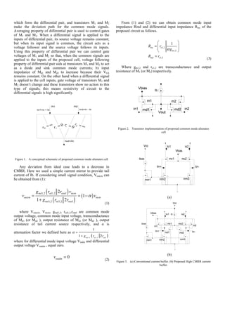
circuit have the same substrate. In these circuits, analog parts
must be resistant to the power supply interference coming from Fig .1 shows the conceptual schematic of the proposed
digital part. These variations which are caused by transient common mode deviating cell. The main idea is using a circuit
currents of digital circuits can cause undesired effects on power in parallel with signal path which has infinitive input resistance
supply rails or analog circuits’ inputs as common mode. Hence to the differential currents and zero to the commons. By using
both CMRR and PSRR play important roles in analog circuits. this idea we can deviates common mode currents and prevent
On the other hand, technology scaling imposes power supply to them from going to the output. On the other hand differential
be lowered. Decreasing power supply imposes some currents cannot flow in this block because of infinite resistance
restrictions on design procedure and harms common-mode to these signals ideally. Fig.2 shows transistor level
rejection ratio (CMRR) and power supply rejection ratio implementing of this idea. This structure is composed of n-type
(PSRR). Hence, for such circuits differential building blocks transistors M1, M2, p-type transistors Md1, Md2 and current
are accepted as a good solution. Therefore it is desired to source of Ib. transistors Md1, Md2, and current source of Ib
978-1-4244-8971-8/10$26.00 c 2010 IEEE
2. which form the differential pair, and transistors M1 and M2 From (1) and (2) we can obtain common mode input
make the deviation path for the common mode signals. impedance Rind and differential input impedance Rinc of the
Averaging property of differential pair is used to control gates proposed circuit as follows.
of M1 and M2. When a differential signal is applied to the
inputs of differential pair, its source voltage remains constant;
but when its input signal is common, the circuit acts as a ⎛ 1 ⎞
voltage follower and the source voltage follows its inputs. Rinc = ⎜ ro1,2 ⎟
⎜ α g m1,2 ⎟
Using this property of differential pair we can control gate ⎝ ⎠
voltages of M1 and M2 so that, when the common signals are Rind = ro1,2
applied to the inputs of the proposed cell, voltage following (3)
property of differential pair aids a) transistors M1 and M2 to act
as a diode and sink common mode currents; b) input Where gm1,2 and ro1,2 are transconductance and output
impedance of Md1 and Md2 to increase because their VGS resistance of M1 (or M2) respectively.
remains constant. On the other hand when a differential signal
is applied to the cell inputs, gate voltage of transistors M1 and
M2 doesn’t change and these transistors show no action to this
type of signals; this means resistivity of circuit to the
differential signals is high significantly.
∞ 0r rd =
rd = rc = c = 0 ∞
Figure 2. Transistor implementation of proposed common mode alienates
cell
Figure 1. A conceptual schematic of proposed common mode alienates cell
Any deviation from ideal case leads to a decrease in
CMRR. Here we used a simple current mirror to provide tail
current of Ib. If considering small signal condition, Voutcm can
be obtained from (1):
voutcm =
( )
g md 1,2 rod 1,2 2rotail vincm
= (1 − α ) vincm
(
1 + g md 1,2 rod 1,2 2rotail ) (1)
(a)
where Voutcm, Vincm, gmd1,2, rod1,2,rotail are common mode
output voltage, common mode input voltage, transconductance
of Md1 (or Md2 ), output resistance of Md1 (or Md2 ), output
resistance of tail current source respectively, and α is
1
attenuation factor we defined here as α =
1 + g md 1, 2 ( rod 1, 2 2 rotail )
where for differential mode input voltage Vindm and differential
output voltage Voutdm , equal zero.
(b)
voutdm = 0
(2) Figure 3. (a) Conventional current buffer. (b) Proposed High CMRR current
buffer.
3. III. APPLICATIONS IV. SIMULATION RESULTS
The proposed structure is very simple, power efficient, and HSPICE simulation were performed using TSMC 0.18µm
has low transistor number. This structure can be applied to the CMOS technology at 1.8 V power supply. The transistors W/L
prevalent structures such as current buffers, folded cascode are shown in table .1. Two circuits are simulated at the same
structures and cause significant improvement in CMRR and condition to make comparison. Fig .5 shows frequency
PSRR in these structures. Here we applied our proposed circuit response of conventional and proposed current buffer.
to the current buffer and folded cascode OTA and compared Differential and common mode input currents are applied to
the CMRR of them both. Fig .3 (a) shows a simple current the both simple and proposed current buffer from in+ and in-
buffer; differential input currents are applied to the Iin1 and Iin2 and output currents are taken from Io1 and Io2. The figure
as shown in the fig .3 (a) and the output taken from Io1 and Io2. exhibits about 12 dB CMRR for proposed current buffer this is
Applying proposed cell to the simple current buffer, the significant enhancement in CMRR value compared to its value
modified current buffer is obtained (See fig .3 (b)). For simple in simple one.
current buffer both differential and common mode input
impedances are obtained from rin=1/gmc where for proposed
current buffer we can obtain input impedance to the differential
and common mode signals as rind=1/gmc and rinc =α/gmc||roc
where gmc and roc are transconductance and output impedance
of Mc1 (or Mc2) respectively.
A conventional folded cascode input stage is shown in fig
.4 (a). Modified version of this is shown in fig .4 (b)
(proposed). Differential and common mode input impedance
for proposed OTA are the same as proposed buffer.
Figure 5. CMRR of the proposed and conventional current buffer
Fig .6 shows the frequency response of the conventional
and proposed folded cascode OTA. Differential and common
mode input currents are applied to the both simple and
proposed current buffer from in+ and in- and output currents
are taken from Io1 and Io2.
As shown in fig .6, the proposed circuit increases (up to 12
dB) the CMRR whereas it preserves CMRR bandwidth.
Preserving CMRR bandwidth is very interesting feature of this
circuit which is not accessible in other similar works.
(a)
Figure 6. CMRR of the proposed and conventional folded cascode OTA
Monte Carlo analysis is performed by 3% variation on
transistors aspect ratio to simulate fabrication condition. Fig .7
shows Mont Carlo analysis for both simple and proposed
(b) current buffer. Comparison of Mont Carlo analysis for simple
and proposed folded cascode OTA is shown in fig .8. As
Figure 4. Conventional folded cascode OTA. (b) Proposed High CMRR shown, CMRR of proposed circuits increased at least 10 dB in
folded cascode OTA.
comparison with the conventional structures.
4. TABLE I. TRANSISTORS ASPECT RATIO
OTA Current Buffer
ELEMENT Proposed conventional Proposed conventional
W L W L W L W L
M1 0.36 µm 0.18 µm NA NA NA NA NA NA
M2 0.36 µm 0.18 µm NA NA NA NA NA NA
Md1 27 µm 0.18 µm NA NA NA NA NA NA
Md2 27 µm 0.18 µm NA NA NA NA NA NA
Mc1 5.4 µm 0.54 µm 5.4 µm 0.54 µm 5.4 µm 0.54 µm 5.4 µm 0.54 µm
Mc2 5.4 µm 0.54 µm 5.4 µm 0.54 µm 5.4 µm 0.54 µm 5.4 µm 0.54 µm
Mm1 3.6 µm 0.54 µm 3.6 µm 0.54 µm 3.6 µm 0.54 µm 3.6 µm 0.54 µm
Mm2 3.6 µm 0.54 µm 3.6 µm 0.54 µm 3.6 µm 0.54 µm 3.6 µm 0.54 µm
MI1 3.6 µm 0.18 µm 3.6 µm 0.18 µm NA NA NA NA
MI2 3.6 µm 0.18 µm 3.6 µm 0.18 µm NA NA NA NA
Mmp1 2.7 µm 0.54 µm 2.7 µm 0.54 µm NA NA NA NA
Mmp2 2.7 µm 0.54 µm 2.7 µm 0.54 µm NA NA NA NA
and cause CMRR to improve in these circuits. This simple and
high effective circuit uses common mode deviating technique
to improve CMRR while preserves CMRR bandwidth which is
a novel technique in order to improve CMRR. Application of
this structure on both current buffer and folded cascode
structures are shown. Simulation results in TSMC 0.18µm
CMOS technology with HSPICE are presented to demonstrate
the validity of the proposed circuit. Mont Carlo analysis is
performed for simulating fabrication condition and
corroborated the appropriate performance of the proposed
circuit.
ACKNOWLEDGMENT
This work is supported by Islamic Azad University, West
Tehran branch.
Figure 7. Monte Carlo analysis of conventional and proposed current buffer. REFERENCES
- -) Simple. - ) Proposed
[1] Shahram Minaei ,I. Cem. Go¨ knar, Oguzhan Cicekoglu, "A new
differential configuration suitable for realization of high CMRR, all-
pass/notch filters," Springer-Verlag, p. 317–326, May 2005.
[2] Allen PE, Holberg DR, CMOS analog circuit design, 2, Ed. New York:
Oxford University Press, 2002.
[3] C.-G. Yu and R. L. Geiger, "Nonideality consideration for high-
precision amplifiers—Analysis of random common-mode rejection
ratio," IEEE Trans. Circuits Syst. I, Fundam. Theory Appl., vol. 40, no.
1, p. 1–12, Jan. 1993.
[4] F. You, S. H. K. Embabi, and E. Sanchez-Sinencio, "On the
commonmode rejection ratio in low voltage operational amplifiers with
complementary N-P input pairs," IEEE Trans. Circuits Syst. II, Analog
Digit.Signal Process., vol. 44, no. 8, p. 678–683, 1997.
[5] Vadim Ivanov, Junlin Zhou, and Igor M. Filanovsky, "A 100-dB CMRR
CMOS Operational Amplifier With Single-Supply Capability," IEEE
TRANSACTIONS ON CIRCUITS AND SYSTEMS—II: EXPRESS
BRIEFS, vol. 54, no. 5, pp. 397-401, May 2005.
[6] Vadim Ivanov, Junlin Zhou, Igor Filanovsky, "A 100 dB CMRR CMOS
Figure 8. Monte Carlo analyses of conventional and proposed folded OTA. - Operational Amplifier With Single-Supply Capability," IEEE., pp. 9-12,
-) Simple. - ) Proposed 2004.
[7] Jaime Rámirez-Angulo, Sandhana Balasubramanian, Antonio J. López-
Martin, and Ramón G. Carvajal, "Low Voltage Differential Input Stage
I. CONCLUSION With Improved CMRR and True Rail-to-Rail Common Mode Input
A novel and simple structure for improving CMRR was Range," IEEE TRANSACTIONS ON CIRCUITS AND SYSTEMS—II:
EXPRESS BRIEFS, vol. 55, no. 12, pp. 1229-1233, Dec. 2008
introduced. As shown, this structure can be added to the
circuitries like folded cascode amplifier, current buffers, etc.;