This paper introduces an optimized hybrid phase disposition PWM control method for cascaded multilevel inverters, which combines low-frequency PWM and high-frequency sinusoidal PWM for improved performance. The proposed technique reduces switching losses by up to 42% and enhances harmonic performance compared to conventional PWM methods. Simulation results demonstrate the effectiveness of the hybrid method across various inverter levels, confirming better efficiency and reliability in operational applications.
![ACEEE International Journal on Electrical and Power Engineering, Vol. 1, No. 1, Jan 2010
Optimized Hybrid Phase Disposition PWM
Control Method for Multilevel Inverter
C.Govindaraju 1 and Dr.K.Baskaran 2
1
Government College of Engineering/Electrical and Electronics Engineering, Salem, India
Email: govindcraju@rediffmail.com
2
Government College of Technology/Computer Science and Engineering, Coimbatore, India
Email: baski_101@yahoo.com
Abstract—This paper presents a new variation of hybrid of this topology is that the modulation, control and
phase disposition pulse width modulation technique suitable protection requirements of each bridge are modular. The
for cascaded multilevel inverter. A hybrid PDPWM is complexity has generally restricted cascaded inverters to
developed based on low frequency PWM and high the higher power range where several switched output
frequency Sinusoidal PWM. An optimized sequential voltage levels are needed and diode clamped structure is
switching scheme introduced in this proposed method to unsuitable because of the difficulty of balancing the series
equalize electro static and electro magnetic stress among the dc capacitor voltages [4].
power devices. It is confirmed that the proposed technique
offers significantly lower switching losses and switching Modulation control of any type of multilevel inverter
transitions. Furthermore, the proposed hybrid PDPWM is quite challenging, and much of the reported research is
offers better harmonic performance compared to its based on somewhat heuristic investigations. Multilevel
conventional PWM counterpart. Simulation results are inverter systems have been compared on the basis of
included in this paper in order to confirm the effectiveness overall performance, with little attempt being made to
of the proposed technique. adapt the best modulation strategy for one topology to
other structures. In this paper, cascaded multilevel inverter
Keywords-Pulse width modulation, phase disposition topology as shown in fig.1 used to investigate the
pulse width modulation, hybrid phase disposition pulse
proposed hybrid phase disposition PWM control scheme.
width modulation, cascaded multilevel inverter.
The proposed method can be equally applied to any
number of levels.
I. INTRODUCTION
Multilevel inverter is an effective solution for II. CONVENTIONAL CARRIER BASED
increasing power and reducing harmonics of ac MODULATION SCHEMES
waveforms. A multilevel inverter has four main
advantages over the conventional bipolar inverter. First,
the voltage stress on each switch is decreased due to series
connection of the switches. Therefore, the rated voltage
and consequently the total power of the inverter could be
safely increased. Second, the rate of change of voltage
(dv/dt) is decreased due to the lower voltage swing of each
switching cycle. Third, harmonic distortion is reduced due
to more output levels. Forth, lower acoustic noise and
electromagnetic interference (EMI) is obtained [1].
Based on these advantages, various circuit topologies
and modulation strategies have been reported for better
utilization of multilevel voltage source inverters.
Multilevel topologies are classified in to three categories:
diode clamped inverters, flying capacitor inverters and
cascaded inverters. The topologies have an equal number
of main switches [2]-[3]. The diode clamped inverter uses
a single dc bus that is subdivided in to number of voltage
levels by a series string of capacitors. A matrix of
semiconductor switches and diodes allows each phase leg
output to be switched to any of these voltage levels. The Fig.1. Schematic diagram of the inverter topology used to
main drawback of diode clamped inverter is the verify the proposed five level (line to neutral) HPDPWM
unbalanced dc link capacitor. It restricts the application of method
diode clamped inverter to five or less number of levels. Multilevel pulse width modulation is based on
Flying capacitor inverter requires the most number of comparison of sinusoidal reference signal with each
capacitors. Cascaded inverter has simple structure but it carrier to determine the voltage level that the inverter
needs various separate dc sources. A particular advantage
36
© 2010 ACEEE
DOI: 01.ijepe.01.01.07](https://image.slidesharecdn.com/07-120921224334-phpapp01/85/Optimized-Hybrid-Phase-Disposition-PWM-Control-Method-for-Multilevel-Inverter-1-320.jpg)
![ACEEE International Journal on Electrical and Power Engineering, Vol. 1, No. 1, Jan 2010
Optimized Hybrid Phase Disposition PWM
Control Method for Multilevel Inverter
C.Govindaraju 1 and Dr.K.Baskaran 2
1
Government College of Engineering/Electrical and Electronics Engineering, Salem, India
Email: govindcraju@rediffmail.com
2
Government College of Technology/Computer Science and Engineering, Coimbatore, India
Email: baski_101@yahoo.com
Abstract—This paper presents a new variation of hybrid of this topology is that the modulation, control and
phase disposition pulse width modulation technique suitable protection requirements of each bridge are modular. The
for cascaded multilevel inverter. A hybrid PDPWM is complexity has generally restricted cascaded inverters to
developed based on low frequency PWM and high the higher power range where several switched output
frequency Sinusoidal PWM. An optimized sequential voltage levels are needed and diode clamped structure is
switching scheme introduced in this proposed method to unsuitable because of the difficulty of balancing the series
equalize electro static and electro magnetic stress among the dc capacitor voltages [4].
power devices. It is confirmed that the proposed technique
offers significantly lower switching losses and switching Modulation control of any type of multilevel inverter
transitions. Furthermore, the proposed hybrid PDPWM is quite challenging, and much of the reported research is
offers better harmonic performance compared to its based on somewhat heuristic investigations. Multilevel
conventional PWM counterpart. Simulation results are inverter systems have been compared on the basis of
included in this paper in order to confirm the effectiveness overall performance, with little attempt being made to
of the proposed technique. adapt the best modulation strategy for one topology to
other structures. In this paper, cascaded multilevel inverter
Keywords-Pulse width modulation, phase disposition topology as shown in fig.1 used to investigate the
pulse width modulation, hybrid phase disposition pulse
proposed hybrid phase disposition PWM control scheme.
width modulation, cascaded multilevel inverter.
The proposed method can be equally applied to any
number of levels.
I. INTRODUCTION
Multilevel inverter is an effective solution for II. CONVENTIONAL CARRIER BASED
increasing power and reducing harmonics of ac MODULATION SCHEMES
waveforms. A multilevel inverter has four main
advantages over the conventional bipolar inverter. First,
the voltage stress on each switch is decreased due to series
connection of the switches. Therefore, the rated voltage
and consequently the total power of the inverter could be
safely increased. Second, the rate of change of voltage
(dv/dt) is decreased due to the lower voltage swing of each
switching cycle. Third, harmonic distortion is reduced due
to more output levels. Forth, lower acoustic noise and
electromagnetic interference (EMI) is obtained [1].
Based on these advantages, various circuit topologies
and modulation strategies have been reported for better
utilization of multilevel voltage source inverters.
Multilevel topologies are classified in to three categories:
diode clamped inverters, flying capacitor inverters and
cascaded inverters. The topologies have an equal number
of main switches [2]-[3]. The diode clamped inverter uses
a single dc bus that is subdivided in to number of voltage
levels by a series string of capacitors. A matrix of
semiconductor switches and diodes allows each phase leg
output to be switched to any of these voltage levels. The Fig.1. Schematic diagram of the inverter topology used to
main drawback of diode clamped inverter is the verify the proposed five level (line to neutral) HPDPWM
unbalanced dc link capacitor. It restricts the application of method
diode clamped inverter to five or less number of levels. Multilevel pulse width modulation is based on
Flying capacitor inverter requires the most number of comparison of sinusoidal reference signal with each
capacitors. Cascaded inverter has simple structure but it carrier to determine the voltage level that the inverter
needs various separate dc sources. A particular advantage
36
© 2010 ACEEE
DOI: 01.ijepe.01.01.07](https://image.slidesharecdn.com/07-120921224334-phpapp01/75/Optimized-Hybrid-Phase-Disposition-PWM-Control-Method-for-Multilevel-Inverter-1-2048.jpg)
![ACEEE International Journal on Electrical and Power Engineering, Vol. 1, No. 1, Jan 2010
should switch to. Carrier based N level PWM operation
consists of N-1 different carriers [5]. The carriers have the
same frequency f c , the same peak to peak amplitude V,
and are disposed so that the bands they occupy are
contiguous. They are defined as
N
Ci = V ((−1) f ( i) yc ( ωc , ϕ) + i − ), i = 1,..., N − 1
2
where y c is a normalized symmetrical triangular carrier
defined as Fig.2.Reference and Carrier Signals for a five level
inverter
1
y c ( ω c , ϕ ) = ( − 1) [ α ] (( α mod 2 ) − 1) + ,
2
ωct + ϕ
α= , ω c = 2 πf c
π
ϕ represents the phase angle of y c . y c is a periodic
function with the period Tc = 2π / ω c .It is shown that
using symmetrical triangular carrier generates less
harmonic distortion at the inverter’s output [6].
Three alternative carrier disposition PWM strategies
are commonly referenced, viz:
Fig.3. Low and High frequency PDPWM pulses at
(i) alternative phase opposition disposition (APOD), mi=0.8 and fc=1050 hz
where each carrier is phase shifted by π from its adjacent
carrier; at two different frequencies, two being commutated at low
(ii) phase opposition disposition (POD), where the frequency, i.e., the fundamental frequency of the output,
carriers above the sinusoidal reference zero point are π while the other two power devices are pulse width
modulated at high frequency. This arrangement causes the
out of phase with those below the zero point;
problem of differential switching losses among the
(iii) phase disposition (PD), where all carriers are in switches.
phase. It is generally accepted that the PD strategy gives
An optimized sequential signal added to the hybrid
rise to the lowest harmonic distortion for the line to line
PWM pulses to overcome this problem. The low and high
voltage [7].
frequency PWM signal are shown in fig.3. An optimized
While the multilevel PWM techniques developed thus hybrid PDPWM method commutates the power switches
far have been extensions of two level PWM methods, the at high frequency and low frequency sequentially. A
multiple levels in a cascaded inverter offer extra degrees common sequential signal and low frequency PWM
of freedom and greater possibilities in terms of device signals are used for all cells in cascaded inverter. A high
utilization, state redundancies, and effective switching frequency SPWM for each cell is obtained by the
frequency. In this paper, novel hybrid multilevel PWM comparison of the rectified modulation waveform with
scheme is presented which take advantage of the special corresponding phase disposition carrier signal. The low
properties available in conventional PWM methods and to frequency PWM signal should be synchronized with the
minimize switching losses with better harmonic modulation waveform. In fig.4, the gate pulses are
performance. Fig.2. shows the carriers and the reference generated by a hybrid PWM controller. This controller is
signals for a five level PWM using PD technique with designed to mix the sequential signal, low frequency
mi=0.8 and carrier frequency f c =1050 hz. PWM and high frequency phase disposition sinusoidal
PWM and to generate the appropriate gate pulses for
cascaded inverter.
III. PROPOSED HYBRID PWM CONTROL METHOD
The proposed hybrid PWM is the combination of low IV. GENERALIZATION OF THE PROPOSED HYBRID PWM
frequency PWM and high frequency SPWM. In each cell TECHNIQUE
of cascaded inverter, the four power devices are operated The previous section has presented the formulation of
an optimized hybrid PDPWM switching pattern of a five
level inverter. For completeness, the generalized
formulation that suits N level inverter is presented.
37
© 2010 ACEEE
DOI: 01.ijepe.01.01.07](https://image.slidesharecdn.com/07-120921224334-phpapp01/85/Optimized-Hybrid-Phase-Disposition-PWM-Control-Method-for-Multilevel-Inverter-2-320.jpg)
![ACEEE International Journal on Electrical and Power Engineering, Vol. 1, No. 1, Jan 2010
distortion (THD) was chosen to evaluate both techniques
and plotted in fig.10. The THD is calculated using (1) and
up to 50th order of harmonics is taken in to account. The
low pass filter and the nature of the highly inductive load
will take care of the higher order of harmonics.
∑
50
n=2
Vn2
THD = (1)
V1
The most accurate method of determining switching losses
is to plot the current and voltage waveform in the power
switch during switching transition and multiplies the
waveform point by point to get an instantaneous power
waveform. The area under the power waveform is the
switching energy at turn on or turn off [8]. In this paper,
the average switching losses are calculated based on the
information of the data sheet, turn on energy losses per
pulse (Eon), turn off energy losses per pulse (Eoff)
including reverse recovery loss and switching
frequency f s = 1 / Ts .
1
Psw = ∑ (Eon + Eoff ) (2)
2πΤs
Fig.4. Optimized Hybrid PDPWM switching pattern for
five level cascaded multilevel inverter
Let N be the number of levels of the cascaded inverter.
M is the number of inverter cells, M=N-1/2. The
modulation index is therefore defined as mi= Am / MAc
and the definition of the frequency ratio mf= fc / fm ,
where f c as carrier frequency and f m as modulating
signal frequency. The modulating signal Am is modified
based on number of levels and modulation index.
A modified sinusoidal modulating signal is then (a)
compared with each phase disposition carrier signal
separately to generate M number of high frequency
sinusoidal PWM signals. A hybrid PWM controller is
used to mix low frequency PWM and the corresponding
th
high frequency SPWM for M inverter cell. This hybrid
th
PWM for M inverter cell is then optimized with
sequential signal in order to equalize switching transitions.
Similarly, hybrid PWM pulses are developed for all cells
in any level cascaded inverter.
V. RESULTS AND DISCUSSION
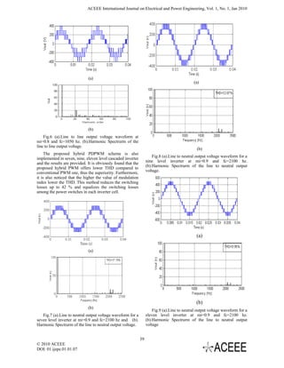
A five level cascaded multilevel inverter model was
built in MATLAB/Simulink software to demonstrate the (b)
feasibility of the hybrid PDPWM and for comparison with Fig.5 (a).Line to neutral output voltage waveform at
conventional PDPWM technique. Fig.5. (a) and (b) shows mi=0.8 and fc=1050 hz. (b).Harmonic Spectrum of the
the output phase and line voltage waveforms with its line to neutral output voltage.
harmonic spectrum at f c =1050 hz, f m =50 hz and
mi=0.8 for a five level inverter. For justifiable
comparison, a performance index namely total harmonic
38
© 2010 ACEEE
DOI: 01.ijepe.01.01.07](https://image.slidesharecdn.com/07-120921224334-phpapp01/85/Optimized-Hybrid-Phase-Disposition-PWM-Control-Method-for-Multilevel-Inverter-3-320.jpg)
![ACEEE International Journal on Electrical and Power Engineering, Vol. 1, No. 1, Jan 2010
Fig.13. Switching loss analysis among the power switches
Fig.10.THD vs.Modulation index for five level inverter at in a cascaded multilevel inverter at mi=0.8 .
fc=1050 hz
VI. CONCLUSION
An optimized hybrid phase disposition PWM control
scheme for cascaded multilevel inverter is proposed in this
paper. A hybrid PDPWM controller is designed to
generate optimum gate pulses for power switches. When
compared with the conventional PWM technique, the
proposed method offers lower switching losses throughout
the entire range of the switching frequency. Voltage and
current stress of power switches in each cell of cascaded
inverter are equalized. Furthermore, the proposed hybrid
PDPWM offers better harmonic performance compared to
its conventional PWM counterpart. Simulation results are
also included for several multilevel inverters using hybrid
PDPWM control method.
REFERENCES
[1] J.Rodriguez, J.S.Lai, an F.Z.peng, “multilevel inverter: A
Fig.11.THD comparision for general cascaded multilevel survey of topologies, controls, and applications,” IEEE
inverter at mi=0.9 and fc=1050 hz Trans. Ind. Electron., Vol.49, no 4, pp. 724-738. Aug.2002.
[2] B.S.Jin, W.K.Lee, T.J.Kim, D.W.Kang, and D.S.Hyun, “ A
Study on the multicarrier PWM methods for voltage
balancing of flying capacitor in the flying capacitor
multilevel inverter, ” in proc.IEEE Ind.
Electron.Conf.Nov.2005, pp.721-726.
[3] B.P.Mcgrath, D.G.Holmes, and T.Meynard, “ Reduced
PWM harmonic distortion for multilevel inverters
operating over a wide modulation range,” IEEE
Trans.Power Electron., Vol.21, no.4, pp.941-949, Jul.2006.
[4] L.M.Tolbert, F.Z.Peng, and T.G.Habetler, “ Multilevel
converters for large electric drives,” IEEE Trans. Ind.
Applicant. Vol.35, pp.36-44, Jan 1999.
[5] B.P.Mcgrath, D.G.Holmes, “Multicarrier PWM strategies
for multilevel inverters,” IEEE Trans.Ind.Electron., Vol
49.no.4, pp 858-867,Aug.2002.
[6] J.Hamman and F.S.van Der merwe, “Voltage harmonics
generated by voltage fed inverters using PWM natural
sampling,” IEEE Trans. Power Electron., Vol PE-3, no.3,
pp.297-302, Jul.1988.
[7] D.G.Holmes and B.P.Mcgrath, “Opportunities for
harmonic cancellation with carrier based PWM for two
Fig.12. Switching Loss comparision for cascaded level and multilevel cascaded inverters”, in conf. prec
multilevel inverter at mi=0.8 . IEEE/ IAS Annual meeting, 1999.
[8] T.J.Kim, D.W.Kang, Y.H.Lee, D.S.Hyun, “The analysis of
conduction and switching losses in multilevel inverter
system”, in proc. of PESC, pp.1363-136
40
© 2010 ACEEE
DOI: 01.ijepe.01.01.07](https://image.slidesharecdn.com/07-120921224334-phpapp01/85/Optimized-Hybrid-Phase-Disposition-PWM-Control-Method-for-Multilevel-Inverter-5-320.jpg)


![Getting Started with Apache Spark: Big Data Made Simple [Free Meetup]](https://cdn.slidesharecdn.com/ss_thumbnails/apachesparkgettingstarted-260203175547-8361bcc3-thumbnail.jpg?width=640&height=640&fit=bounds)
