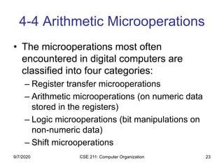
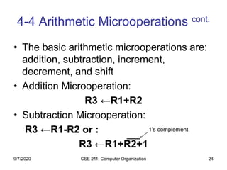
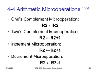
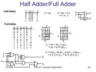
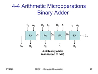
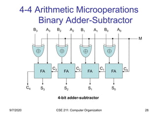
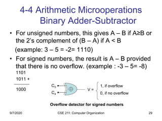
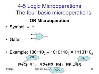
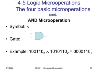
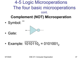
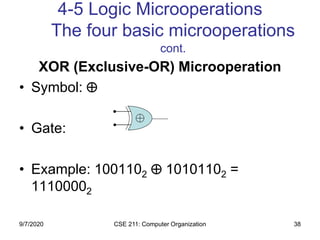
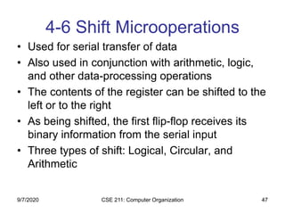
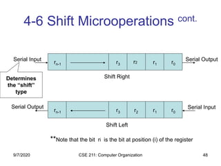
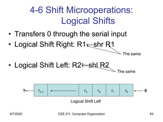
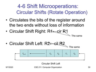
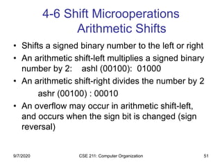
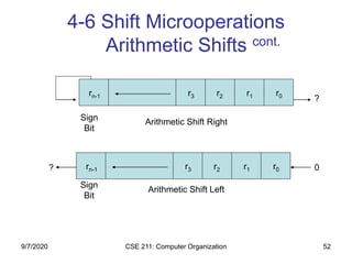
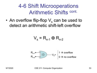
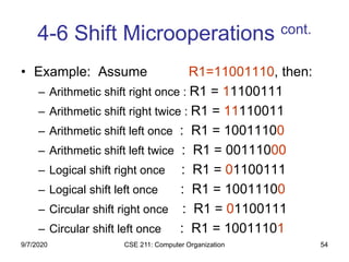
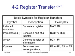
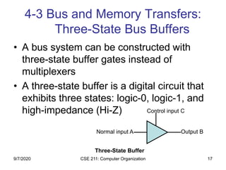
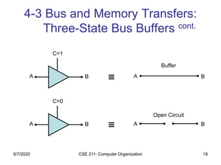
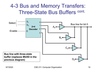
The document discusses register transfer language (RTL) and microoperations in computer organization. It covers topics like register transfer, bus and memory transfers, arithmetic operations, logic operations, and shift operations. Register transfer involves transferring data between computer registers using microoperations. Common bus systems and three-state buffers are used to transfer data between multiple registers. Memory transfers read from and write to memory locations specified by an address register. Arithmetic operations include addition, subtraction, incrementing and decrementing using half adders, full adders and binary adders. Logic operations include AND, OR and NOT gates.

![CSE 211: Computer Organization 20
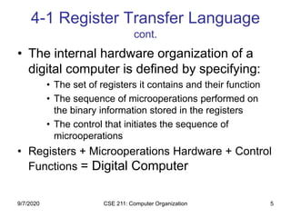
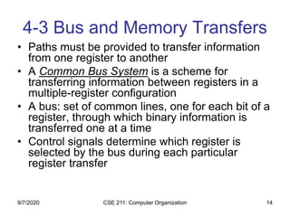
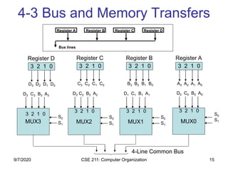
4-3 Bus and Memory Transfers:
Memory Transfer
• Memory read : Transfer from memory
• Memory write : Transfer to memory
• Data being read or wrote is called a memory
word (called M)
• It is necessary to specify the address of M when
writing /reading memory
• This is done by enclosing the address in square
brackets following the letter M
• Example: M[0016] : the memory contents at
address 0x0016
9/7/2020](https://image.slidesharecdn.com/chapter4-200907163817/85/Register-transfer-and-microoperations-20-320.jpg)
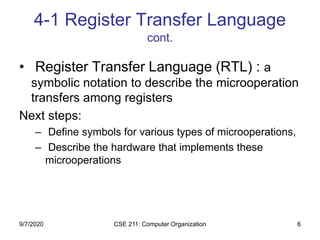
![CSE 211: Computer Organization 21
4-3 Bus and Memory Transfers:
Memory Transfer cont.
• Assume that the address of a memory unit
is stored in a register called the Address
Register AR
• Lets represent a Data Register with DR,
then:
• Read: DR ← M[AR]
• Write: M[AR] ← DR
9/7/2020](https://image.slidesharecdn.com/chapter4-200907163817/85/Register-transfer-and-microoperations-21-320.jpg)
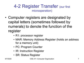
![CSE 211: Computer Organization 22
4-3 Bus and Memory Transfers:
Memory Transfer cont.
AR
x12
x0C
x0E
x10
x12
x14
x16
x18
19
34
45
66
0
13
22R1←M[AR]
R1
100
R1
66
RAM
R1
100
9/7/2020](https://image.slidesharecdn.com/chapter4-200907163817/85/Register-transfer-and-microoperations-22-320.jpg)