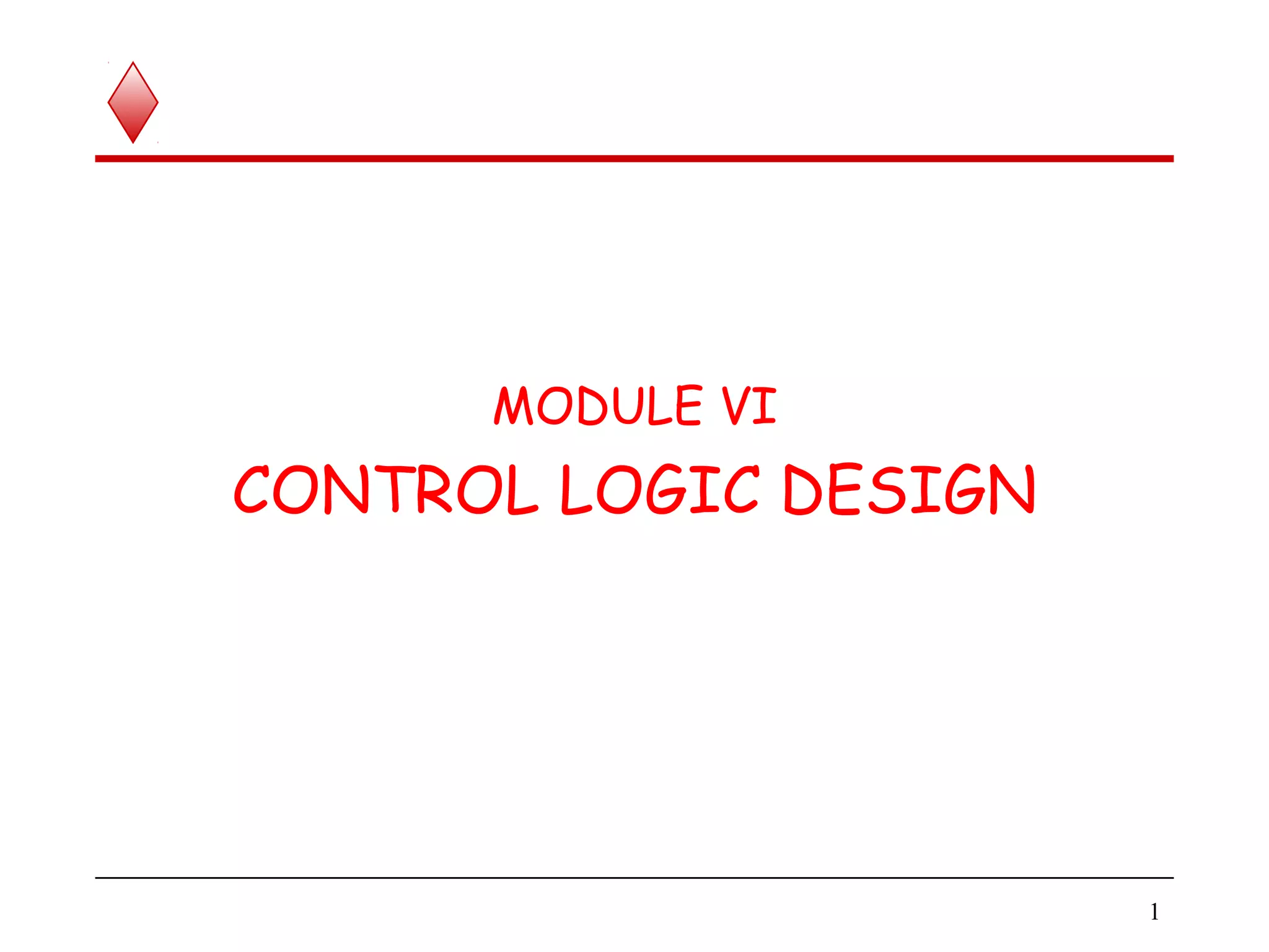
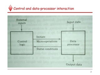
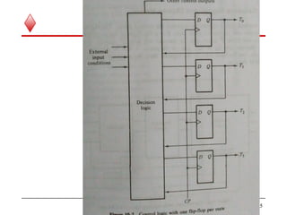
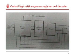
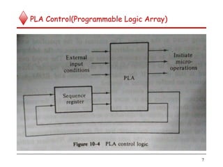
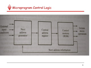
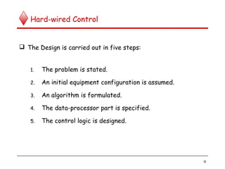
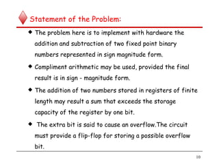
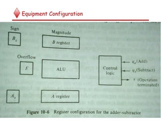
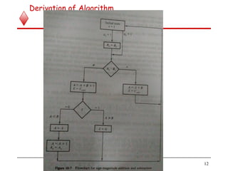
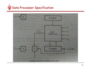
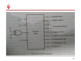
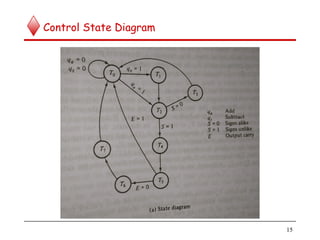
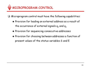
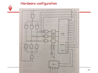
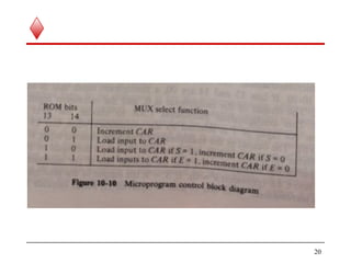
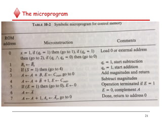
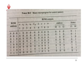
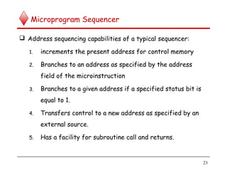
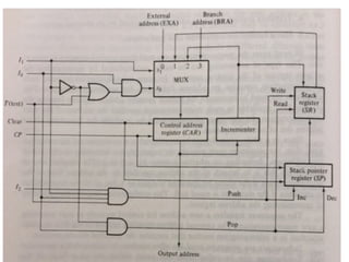
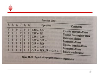
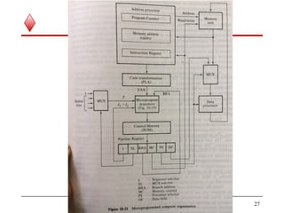
MODULE VI
CONTROL LOGIC DESIGN
1
Control and data-processor interaction
2
Control Organization
 Four Methods:
1. One flip-flop per state method
2. Sequence register and decoder method.
3. PLA control
4. Microprogram control
3
One flip-flop per state method
4
5
Control logic with sequence register and decoder
6
PLA Control(Programmable Logic Array)
7
Microprogram Control Logic
8
Hard-wired Control
 The Design is carried out in five steps:
1. The problem is stated.
2. An initial equipment configuration is assumed.
3. An algorithm is formulated.
4. The data-processor part is specified.
5. The control logic is designed.
9
Statement of the Problem:
 The problem here is to implement with hardware the
addition and subtraction of two fixed point binary
numbers represented in sign magnitude form.
 Compliment arithmetic may be used, provided the final
result is in sign - magnitude form.
 The addition of two numbers stored in registers of finite
length may result a sum that exceeds the storage
capacity of the register by one bit.
 The extra bit is said to cause an overflow.The circuit
must provide a flip-flop for storing a possible overflow
bit.
10
Equipment Configuration
11
Derivation of Algorithm
12
Data Processor Specification
13
14
Control State Diagram
15
16
Design of Hard-wired Control
17
MICROPROGRAM CONTROL
18
Hardware configuration
19
20
The microprogram
21
22
Microprogram Sequencer
 Address sequencing capabilities of a typical sequencer:
1. increments the present address for control memory
2. Branches to an address as specified by the address
field of the microinstruction
3. Branches to a given address if a specified status bit is
equal to 1.
4. Transfers control to a new address as specified by an
external source.
5. Has a facility for subroutine call and returns.
23
24
25
Microprogrammed CPU Organization
26
27

Module vi