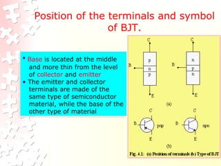
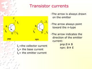
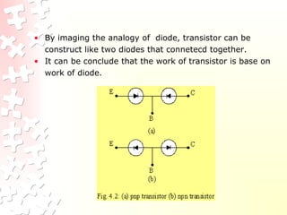
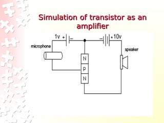
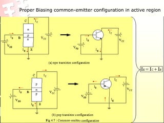
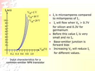
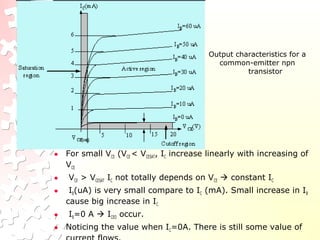
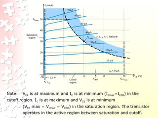
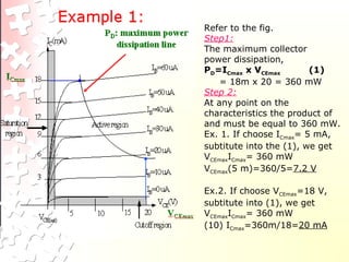
SlideShare a Scribd company logo
1 of 44
Bipolar Junction TransistorBipolar Junction Transistor
(BJT)(BJT)
CHAPTER 3
IntroductionIntroduction
• The basic of electronic system nowadays is
semiconductor device.
• The famous and commonly use of this device
is BJTs
(Bipolar Junction Transistors).
• It can be use as amplifier and logic switches.
• BJT consists of three terminal:
 collector : C
 base : B
emitter : E
• Two types of BJT : pnp and npn
Transistor ConstructionTransistor Construction
• 3 layer semiconductor device consisting:
• 2 n- and 1 p-type layers of material  npn transistor
• 2 p- and 1 n-type layers of material pnp transistor
• The term bipolar reflects the fact that holes and
electrons participate in the injection process into the
oppositely polarized material
• A single pn junction has two different types of bias:
• forward bias
• reverse bias
• Thus, a two-pn-junction device has four types of bias.
Position of the terminals and symbol
of BJT.
• Base is located at the middle
and more thin from the level
of collector and emitter
• The emitter and collector
terminals are made of the
same type of semiconductor
material, while the base of the
other type of material
• Base is located at the middle
and more thin from the level
of collector and emitter
• The emitter and collector
terminals are made of the
same type of semiconductor
material, while the base of the
other type of material
Transistor currents
-The arrow is always drawn
on the emitter
-The arrow always point
toward the n-type
-The arrow indicates the
direction of the emitter
current:
pnp:E B
npn: B E
IC=the collector current
IB= the base current
IE= the emitter current
• By imaging the analogy of diode, transistor can be
construct like two diodes that connetecd together.
• It can be conclude that the work of transistor is base on
work of diode.
Transistor OperationTransistor Operation
• The basic operation will be described using the pnp
transistor. The operation of the pnp transistor is
exactly the same if the roles played by the electron
and hole are interchanged.
• One p-n junction of a transistor is reverse-biased,
whereas the other is forward-biased.
Forward-biased junction
of a pnp transistor
Reverse-biased junction
of a pnp transistor
• Both biasing potentials have been applied to a pnp
transistor and resulting majority and minority carrier
flows indicated.
• Majority carriers (+) will diffuse across the forward-
biased p-n junction into the n-type material.
• A very small number of carriers (+) will through n-type
material to the base terminal. Resulting IB is typically in
order of microamperes.
• The large number of majority carriers will diffuse across
the reverse-biased junction into the p-type material
connected to the collector terminal.
• Majority carriers can cross the reverse-biased
junction because the injected majority carriers will
appear as minority carriers in the n-type material.
• Applying KCL to the transistor :
IE = IC + IB
• The comprises of two components – the majority
and minority carriers
IC = ICmajority + ICOminority
• ICO – IC current with emitter terminal open and is
called leakage current.
Common-Base ConfigurationCommon-Base Configuration
• Common-base terminology is derived from the fact that
the :
- base is common to both input and output of the
configuration.
- base is usually the terminal closest to or at
ground potential.
• All current directions will refer to conventional (hole)
flow and the arrows in all electronic symbols have a
direction defined by this convention.
• Note that the applied biasing (voltage sources) are such
as to establish current in the direction indicated for
each branch.
• To describe the behavior of common-base amplifiers
requires two set of characteristics:
- Input or driving point characteristics.
- Output or collector characteristics
• The output characteristics has 3 basic regions:
- Active region –defined by the biasing arrangements
- Cutoff region – region where the collector current is 0A
- Saturation region- region of the characteristics to the left
of VCB = 0V
• The curves (output characteristics) clearly indicate
that a first approximation to the relationship between
IE and IC in the active region is given by
IC ≈IE
• Once a transistor is in the ‘on’ state, the base-emitter
voltage will be assumed to be
VBE = 0.7V
• In the dc mode the level of IC and IE due to the
majority carriers are related by a quantity called
alpha
α=
IC = αIE + ICBO
• It can then be summarize to IC = αIE (ignore ICBO due
to small value)
• For ac situations where the point of operation moves
on the characteristics curve, an ac alpha defined by
• Alpha a common base current gain factorcommon base current gain factor that shows
the efficiency by calculating the current percent from
current flow from emitter to collector.The value of α is
typical from 0.9 ~ 0.998.
E
C
I
I
E
C
I
I
∆
∆
=α
BiasingBiasing
• Proper biasing CB configuration in active region by
approximation IC ≈ IE (IB ≈ 0 uA)
Transistor as an amplifierTransistor as an amplifier
Simulation of transistor as anSimulation of transistor as an
amplifieramplifier
Common-Emitter ConfigurationCommon-Emitter Configuration
• It is called common-emitter configuration since :
- emitter is common or reference to both input and
output terminals.
- emitter is usually the terminal closest to or at
ground
potential.
• Almost amplifier design is using connection of CE duedue
to the high gain for current and voltageto the high gain for current and voltage.
• Two set of characteristics are necessary to describe
the behavior for CE ;input (base terminal) and output
(collector terminal) parameters.
Proper Biasing common-emitter configuration in active region
Input characteristics for a
common-emitter NPN transistorcommon-emitter NPN transistor
• IB is microamperes compared
to miliamperes of IC.
• IB will flow when VBE > 0.7V
for silicon and 0.3V for
germanium
• Before this value IB is very
small and no IB.
• Base-emitter junction is
forward bias
• Increasing VCE will reduce IB
for different values.
Output characteristics for a
common-emitter npn
transistor
• For small VCE (VCE < VCESAT, IC increase linearly with increasing of
VCE
• VCE > VCESAT IC not totally depends on VCE  constant IC
• IB(uA) is very small compare to IC (mA). Small increase in IB
cause big increase in IC
• IB=0 A  ICEO occur.
• Noticing the value when IC=0A. There is still some value of
Beta (β) or amplification factoramplification factor
• The ratio of dc collector current (IC) to the dc base
current (IB) is dc beta (βdc ) which is dc current gain
where IC and IB are determined at a particular operating
point, Q-point (quiescent point).
• It’s define by the following equation:
30 < βdc < 300  2N3904
• On data sheet, ββdcdc==hhFEFE with hh is derived from ac hybrid
equivalent cct. FE are derived from forward-current
amplification and common-emitter configuration
respectively.
• For ac conditions an ac beta has been defined as the
changes of collector current (IC) compared to the
changes of base current (IB) where IC and IB are
determined at operating point.
• On data sheet, βac=hfe
• It can defined by the following equation:
ExampleExample
From output characteristics of common
emitter configuration, find βac and βdc with an
Operating point at IB=25 µA and VCE =7.5V.
Solution:
Relationship analysis between αα and ββ
Common – Collector ConfigurationCommon – Collector Configuration
• Also called emitter-follower (EF).
• It is called common-emitter configuration since both the
signal source and the load share the collector terminal
as a common connection point.
• The output voltage is obtained at emitter terminal.
• The input characteristic of common-collector
configuration is similar with common-emitter.
configuration.
• Common-collector circuit configuration is provided with
the load resistor connected from emitter to ground.
• It is used primarily for impedance-matching purpose
since it has high input impedance and low output
impedance.
Notation and symbols used with the common-collector configuration:
(a) pnp transistor ; (b) npn transistor.
• For the common-collector configuration, the output
characteristics are a plot of IE vs VCE for a range of values of IB.
Limits of OperationLimits of Operation
• Many BJT transistor used as an amplifier. Thus it is
important to notice the limits of operations.
• At least 3 maximum values is mentioned in data sheet.
• There are:
a) Maximum power dissipation at collector: PCmax
or PD
b) Maximum collector-emitter voltage: VCEmax
sometimes named as VBR(CEO) or VCEO.
c) Maximum collector current: ICmax
• There are few rules that need to be followed for BJT
transistor used as an amplifier. The rules are:
i) transistor need to be operate in active region!
ii) IC < ICmax
ii) PC < PCmax
Note: VCE is at maximum and IC is at minimum (ICmax=ICEO) in the
cutoff region. IC is at maximum and VCE is at minimum
(VCE max = VCEsat = VCEO) in the saturation region. The transistor
operates in the active region between saturation and cutoff.
Refer to the fig.
Step1:
The maximum collector
power dissipation,
PD=ICmax x VCEmax (1)
= 18m x 20 = 360 mW
Step 2:
At any point on the
characteristics the product of
and must be equal to 360 mW.
Ex. 1. If choose ICmax= 5 mA,
subtitute into the (1), we get
VCEmaxICmax= 360 mW
VCEmax(5 m)=360/5=7.2 V
Ex.2. If choose VCEmax=18 V,
subtitute into (1), we get
VCEmaxICmax= 360 mW
(10) ICmax=360m/18=20 mA
Derating PDerating PDmaxDmax
• PDmax is usually specified at 25°C.
• The higher temperature goes, the less is PDmax
• Example;
• A derating factor of 2mW/°C indicates the power
dissipation is reduced 2mW each degree centigrade
increase of temperature.
ExampleExample
Transistor 2N3904 used in the circuit with
VCE=20 V. This circuit used at temperature
1250
C. Calculate the new maximum IC.
Transistor 2N3904 have maximum power
dissipation is 625 mW. Derating factor is
5mW/0C.
SolutionSolution
• Step 1:
Temperature increase : 1250C
– 250
C = 1000
C
• Step 2:
Derate transistor : 5 mW/0
C x 1000
C = 500 mW
• Step 3:
Maximum power dissipation at 1250
C = 625 mW–500
mW=125 mW.
• Step 4:
Thus ICmax = PCmax / VCE=125m/20 = 6.25 mA.
• Step 5:
Draw the new line of power dissipation at 1250
C .
ExampleExample
The parameters of transistor 2N3055 as follows:
- Maximum power dissipation @ 250C=115 W
- Derate factor=0.66 mW/0
C.
This transistor used at temperature 780
C.
Find the new maximum value of power dissipation.
Find the set of new maximum of IC if VCE=10V,
20V and 40 V.
SolutionSolution
• Step 1:
Temperature increase : 780
C – 250
C = 530
C
• Step 2:
Derate transistor : 0.66mW/0
C x 530
C = 35 mW
• Step 3:
Maximum power dissipation at 780
C = 115W– 35W=80
mW.
• Step 4:
ICmax = PCmax / VCE=80m/10 = 8 mA (point C)
ICmax = PCmax / VCE=80m/20 = 4 mA. (point B)
ICmax = PCmax / VCE=80m/40 = 2 mA (point A)
Step 5:
Draw the new line of power dissipation at 780
C .
Transistor Specification SheetTransistor Specification Sheet
Transistor Terminal Identification
Transistor Testing
1. Curve Tracer
Provides a graph of the characteristic curves.
2. DMM
Some DMM’s will measure βDC or HFE.
3. Ohmmeter

More Related Content

What's hot (20)

Operational amplifier
Operational amplifierOperational amplifier
Operational amplifier
 
Bipolar Junction Transistor (BJT).pptx
Bipolar Junction Transistor (BJT).pptxBipolar Junction Transistor (BJT).pptx
Bipolar Junction Transistor (BJT).pptx
 
Transistor as a switch
Transistor as a switch Transistor as a switch
Transistor as a switch
 
Tunnel diode
Tunnel diodeTunnel diode
Tunnel diode
 
Field Effect Transistor ppt
Field Effect Transistor pptField Effect Transistor ppt
Field Effect Transistor ppt
 
Field Effect Transistor
Field Effect TransistorField Effect Transistor
Field Effect Transistor
 
Power amplifiers
Power amplifiersPower amplifiers
Power amplifiers
 
Presentation on bjt configuration
Presentation on bjt configuration Presentation on bjt configuration
Presentation on bjt configuration
 
Transistors
Transistors Transistors
Transistors
 
Diode
DiodeDiode
Diode
 
Zener diodes
Zener diodesZener diodes
Zener diodes
 
Mosfet
MosfetMosfet
Mosfet
 
Oscillators
OscillatorsOscillators
Oscillators
 
Load line analysis
Load line analysisLoad line analysis
Load line analysis
 
Hybrid Parameter in BJT
Hybrid Parameter in BJTHybrid Parameter in BJT
Hybrid Parameter in BJT
 
Bipolar Junction Transistor (BJT) DC and AC Analysis
Bipolar Junction Transistor (BJT) DC and AC AnalysisBipolar Junction Transistor (BJT) DC and AC Analysis
Bipolar Junction Transistor (BJT) DC and AC Analysis
 
EST 130, Transistor Biasing and Amplification.
EST 130, Transistor Biasing and Amplification.EST 130, Transistor Biasing and Amplification.
EST 130, Transistor Biasing and Amplification.
 
Mosfet
MosfetMosfet
Mosfet
 
Unit-1 Power Semiconductor devices
Unit-1 Power Semiconductor devicesUnit-1 Power Semiconductor devices
Unit-1 Power Semiconductor devices
 
JFET
JFETJFET
JFET
 

Viewers also liked

TRANSISTORS
 TRANSISTORS TRANSISTORS
TRANSISTORSAJAL A J
 
Ppt presentation on FET
Ppt presentation on  FETPpt presentation on  FET
Ppt presentation on FETSkmdbg
 
Basic logic gates
Basic logic gatesBasic logic gates
Basic logic gatesKumar
 
EE201 -Chapter 6
EE201 -Chapter 6EE201 -Chapter 6
EE201 -Chapter 6ruhiyah
 
EE201 -Chapter 4
EE201 -Chapter 4 EE201 -Chapter 4
EE201 -Chapter 4 ruhiyah
 
EE201 - Chapter 3 (BJT)
EE201 - Chapter 3 (BJT)EE201 - Chapter 3 (BJT)
EE201 - Chapter 3 (BJT)ruhiyah
 
Sc and oc test on transformer
Sc and oc test on transformerSc and oc test on transformer
Sc and oc test on transformerPooja Dubey
 
open circuit and short circuit test on transformer
open circuit and short circuit test on transformeropen circuit and short circuit test on transformer
open circuit and short circuit test on transformerMILAN MANAVAR
 
Testing of transformer
Testing of transformerTesting of transformer
Testing of transformervikasgupta1965
 
Transistor as an amplifier
Transistor as an amplifierTransistor as an amplifier
Transistor as an amplifierAnshu Kumar
 
Physics investigatory class 12
Physics investigatory class 12Physics investigatory class 12
Physics investigatory class 12Himanshu Soni
 
number system school ppt ninth class
number system school ppt ninth classnumber system school ppt ninth class
number system school ppt ninth classManan Jain
 
Computer number systems
Computer number systemsComputer number systems
Computer number systemsRevi Shahini
 
Power electronics 12. application devices
Power electronics   12. application devicesPower electronics   12. application devices
Power electronics 12. application devicesBurdwan University
 

Viewers also liked (20)

TRANSISTORS
 TRANSISTORS TRANSISTORS
TRANSISTORS
 
Mosfet
MosfetMosfet
Mosfet
 
Ppt presentation on FET
Ppt presentation on  FETPpt presentation on  FET
Ppt presentation on FET
 
Basic logic gates
Basic logic gatesBasic logic gates
Basic logic gates
 
EE201 -Chapter 6
EE201 -Chapter 6EE201 -Chapter 6
EE201 -Chapter 6
 
Lecture 8 bjt_1
Lecture 8 bjt_1Lecture 8 bjt_1
Lecture 8 bjt_1
 
EE201 -Chapter 4
EE201 -Chapter 4 EE201 -Chapter 4
EE201 -Chapter 4
 
EE201 - Chapter 3 (BJT)
EE201 - Chapter 3 (BJT)EE201 - Chapter 3 (BJT)
EE201 - Chapter 3 (BJT)
 
Sc and oc test on transformer
Sc and oc test on transformerSc and oc test on transformer
Sc and oc test on transformer
 
open circuit and short circuit test on transformer
open circuit and short circuit test on transformeropen circuit and short circuit test on transformer
open circuit and short circuit test on transformer
 
Testing of transformer
Testing of transformerTesting of transformer
Testing of transformer
 
Transistor as an amplifier
Transistor as an amplifierTransistor as an amplifier
Transistor as an amplifier
 
Number system
Number systemNumber system
Number system
 
Physics investigatory class 12
Physics investigatory class 12Physics investigatory class 12
Physics investigatory class 12
 
number system school ppt ninth class
number system school ppt ninth classnumber system school ppt ninth class
number system school ppt ninth class
 
Computer number systems
Computer number systemsComputer number systems
Computer number systems
 
Number System
Number SystemNumber System
Number System
 
Solenoids
SolenoidsSolenoids
Solenoids
 
Power electronics 12. application devices
Power electronics   12. application devicesPower electronics   12. application devices
Power electronics 12. application devices
 
Triac (industrial electronic)
Triac (industrial electronic)Triac (industrial electronic)
Triac (industrial electronic)
 

Similar to 3.bipolar junction transistor (bjt)

Transistor Fundamentals
Transistor FundamentalsTransistor Fundamentals
Transistor FundamentalsJay Baria
 
Bipolar Transistor
Bipolar TransistorBipolar Transistor
Bipolar TransistorUMAR ALI
 
Transistor Configuration
Transistor Configuration Transistor Configuration
Transistor Configuration Smit Shah
 
Bjt(common base ,emitter,collector) from university of central punjab
Bjt(common base ,emitter,collector) from university of central punjabBjt(common base ,emitter,collector) from university of central punjab
Bjt(common base ,emitter,collector) from university of central punjabKhawaja Shazy
 
Chapter 6: Bipolar Junction Transistors (BJTs)
Chapter 6: Bipolar Junction Transistors (BJTs)Chapter 6: Bipolar Junction Transistors (BJTs)
Chapter 6: Bipolar Junction Transistors (BJTs)JeremyLauKarHei
 
Bipolar junction transisitors.ppt
Bipolar junction transisitors.pptBipolar junction transisitors.ppt
Bipolar junction transisitors.pptsaba145
 
BJT Basic and Biasing-Abridged(1).pptx
BJT Basic and Biasing-Abridged(1).pptxBJT Basic and Biasing-Abridged(1).pptx
BJT Basic and Biasing-Abridged(1).pptxNimishDuggal1
 
Transistors handout
Transistors handoutTransistors handout
Transistors handoutEng Mahamed
 
prestationonbipolarjunciontransistor-151128084200-lva1-app6891.pptx
prestationonbipolarjunciontransistor-151128084200-lva1-app6891.pptxprestationonbipolarjunciontransistor-151128084200-lva1-app6891.pptx
prestationonbipolarjunciontransistor-151128084200-lva1-app6891.pptxShruthiShillu1
 
Unit - IV(i) BJT.pdf
Unit - IV(i) BJT.pdfUnit - IV(i) BJT.pdf
Unit - IV(i) BJT.pdfSachinNaagar4
 
BIPOLAR JUNCTION TRANSISTOR
BIPOLAR JUNCTION TRANSISTORBIPOLAR JUNCTION TRANSISTOR
BIPOLAR JUNCTION TRANSISTORssuserb29892
 

Similar to 3.bipolar junction transistor (bjt) (20)

bjt1.ppt
bjt1.pptbjt1.ppt
bjt1.ppt
 
bjt1.ppt
bjt1.pptbjt1.ppt
bjt1.ppt
 
bjt1.ppt
bjt1.pptbjt1.ppt
bjt1.ppt
 
Bjt
BjtBjt
Bjt
 
Transistor Fundamentals
Transistor FundamentalsTransistor Fundamentals
Transistor Fundamentals
 
BJT.ppt
BJT.pptBJT.ppt
BJT.ppt
 
Bipolar Transistor
Bipolar TransistorBipolar Transistor
Bipolar Transistor
 
Transistor Configuration
Transistor Configuration Transistor Configuration
Transistor Configuration
 
Bjt(common base ,emitter,collector) from university of central punjab
Bjt(common base ,emitter,collector) from university of central punjabBjt(common base ,emitter,collector) from university of central punjab
Bjt(common base ,emitter,collector) from university of central punjab
 
Chapter 6: Bipolar Junction Transistors (BJTs)
Chapter 6: Bipolar Junction Transistors (BJTs)Chapter 6: Bipolar Junction Transistors (BJTs)
Chapter 6: Bipolar Junction Transistors (BJTs)
 
Chapter 4 bjt
Chapter 4 bjtChapter 4 bjt
Chapter 4 bjt
 
Bipolar junction transisitors.ppt
Bipolar junction transisitors.pptBipolar junction transisitors.ppt
Bipolar junction transisitors.ppt
 
BJT Basic and Biasing-Abridged(1).pptx
BJT Basic and Biasing-Abridged(1).pptxBJT Basic and Biasing-Abridged(1).pptx
BJT Basic and Biasing-Abridged(1).pptx
 
Transistors handout
Transistors handoutTransistors handout
Transistors handout
 
ADE UNIT-2.pptx
ADE UNIT-2.pptxADE UNIT-2.pptx
ADE UNIT-2.pptx
 
prestationonbipolarjunciontransistor-151128084200-lva1-app6891.pptx
prestationonbipolarjunciontransistor-151128084200-lva1-app6891.pptxprestationonbipolarjunciontransistor-151128084200-lva1-app6891.pptx
prestationonbipolarjunciontransistor-151128084200-lva1-app6891.pptx
 
Unit - IV(i) BJT.pdf
Unit - IV(i) BJT.pdfUnit - IV(i) BJT.pdf
Unit - IV(i) BJT.pdf
 
BIPOLAR JUNCTION TRANSISTOR
BIPOLAR JUNCTION TRANSISTORBIPOLAR JUNCTION TRANSISTOR
BIPOLAR JUNCTION TRANSISTOR
 
BJT CB Configuration
BJT CB ConfigurationBJT CB Configuration
BJT CB Configuration
 
Unit 3
Unit 3Unit 3
Unit 3
 

Recently uploaded

A Year of the Servo Reboot: Where Are We Now?
A Year of the Servo Reboot: Where Are We Now?A Year of the Servo Reboot: Where Are We Now?
A Year of the Servo Reboot: Where Are We Now?Igalia
 
04-2024-HHUG-Sales-and-Marketing-Alignment.pptx
04-2024-HHUG-Sales-and-Marketing-Alignment.pptx04-2024-HHUG-Sales-and-Marketing-Alignment.pptx
04-2024-HHUG-Sales-and-Marketing-Alignment.pptxHampshireHUG
 
Mastering MySQL Database Architecture: Deep Dive into MySQL Shell and MySQL R...
Mastering MySQL Database Architecture: Deep Dive into MySQL Shell and MySQL R...Mastering MySQL Database Architecture: Deep Dive into MySQL Shell and MySQL R...
Mastering MySQL Database Architecture: Deep Dive into MySQL Shell and MySQL R...Miguel Araújo
 
Automating Google Workspace (GWS) & more with Apps Script
Automating Google Workspace (GWS) & more with Apps ScriptAutomating Google Workspace (GWS) & more with Apps Script
Automating Google Workspace (GWS) & more with Apps Scriptwesley chun
 
[2024]Digital Global Overview Report 2024 Meltwater.pdf
[2024]Digital Global Overview Report 2024 Meltwater.pdf[2024]Digital Global Overview Report 2024 Meltwater.pdf
[2024]Digital Global Overview Report 2024 Meltwater.pdfhans926745
 
Artificial Intelligence: Facts and Myths
Artificial Intelligence: Facts and MythsArtificial Intelligence: Facts and Myths
Artificial Intelligence: Facts and MythsJoaquim Jorge
 
Driving Behavioral Change for Information Management through Data-Driven Gree...
Driving Behavioral Change for Information Management through Data-Driven Gree...Driving Behavioral Change for Information Management through Data-Driven Gree...
Driving Behavioral Change for Information Management through Data-Driven Gree...Enterprise Knowledge
 
Presentation on how to chat with PDF using ChatGPT code interpreter
Presentation on how to chat with PDF using ChatGPT code interpreterPresentation on how to chat with PDF using ChatGPT code interpreter
Presentation on how to chat with PDF using ChatGPT code interpreternaman860154
 
08448380779 Call Girls In Civil Lines Women Seeking Men
08448380779 Call Girls In Civil Lines Women Seeking Men08448380779 Call Girls In Civil Lines Women Seeking Men
08448380779 Call Girls In Civil Lines Women Seeking MenDelhi Call girls
 
Tata AIG General Insurance Company - Insurer Innovation Award 2024
Tata AIG General Insurance Company - Insurer Innovation Award 2024Tata AIG General Insurance Company - Insurer Innovation Award 2024
Tata AIG General Insurance Company - Insurer Innovation Award 2024The Digital Insurer
 
Boost Fertility New Invention Ups Success Rates.pdf
Boost Fertility New Invention Ups Success Rates.pdfBoost Fertility New Invention Ups Success Rates.pdf
Boost Fertility New Invention Ups Success Rates.pdfsudhanshuwaghmare1
 
How to convert PDF to text with Nanonets
How to convert PDF to text with NanonetsHow to convert PDF to text with Nanonets
How to convert PDF to text with Nanonetsnaman860154
 
08448380779 Call Girls In Diplomatic Enclave Women Seeking Men
08448380779 Call Girls In Diplomatic Enclave Women Seeking Men08448380779 Call Girls In Diplomatic Enclave Women Seeking Men
08448380779 Call Girls In Diplomatic Enclave Women Seeking MenDelhi Call girls
 
Advantages of Hiring UIUX Design Service Providers for Your Business
Advantages of Hiring UIUX Design Service Providers for Your BusinessAdvantages of Hiring UIUX Design Service Providers for Your Business
Advantages of Hiring UIUX Design Service Providers for Your BusinessPixlogix Infotech
 
Breaking the Kubernetes Kill Chain: Host Path Mount
Breaking the Kubernetes Kill Chain: Host Path MountBreaking the Kubernetes Kill Chain: Host Path Mount
Breaking the Kubernetes Kill Chain: Host Path MountPuma Security, LLC
 
A Domino Admins Adventures (Engage 2024)
A Domino Admins Adventures (Engage 2024)A Domino Admins Adventures (Engage 2024)
A Domino Admins Adventures (Engage 2024)Gabriella Davis
 
GenCyber Cyber Security Day Presentation
GenCyber Cyber Security Day PresentationGenCyber Cyber Security Day Presentation
GenCyber Cyber Security Day PresentationMichael W. Hawkins
 
08448380779 Call Girls In Greater Kailash - I Women Seeking Men
08448380779 Call Girls In Greater Kailash - I Women Seeking Men08448380779 Call Girls In Greater Kailash - I Women Seeking Men
08448380779 Call Girls In Greater Kailash - I Women Seeking MenDelhi Call girls
 
Workshop - Best of Both Worlds_ Combine KG and Vector search for enhanced R...
Workshop - Best of Both Worlds_ Combine  KG and Vector search for  enhanced R...Workshop - Best of Both Worlds_ Combine  KG and Vector search for  enhanced R...
Workshop - Best of Both Worlds_ Combine KG and Vector search for enhanced R...Neo4j
 
Finology Group – Insurtech Innovation Award 2024
Finology Group – Insurtech Innovation Award 2024Finology Group – Insurtech Innovation Award 2024
Finology Group – Insurtech Innovation Award 2024The Digital Insurer
 

Recently uploaded (20)

A Year of the Servo Reboot: Where Are We Now?
A Year of the Servo Reboot: Where Are We Now?A Year of the Servo Reboot: Where Are We Now?
A Year of the Servo Reboot: Where Are We Now?
 
04-2024-HHUG-Sales-and-Marketing-Alignment.pptx
04-2024-HHUG-Sales-and-Marketing-Alignment.pptx04-2024-HHUG-Sales-and-Marketing-Alignment.pptx
04-2024-HHUG-Sales-and-Marketing-Alignment.pptx
 
Mastering MySQL Database Architecture: Deep Dive into MySQL Shell and MySQL R...
Mastering MySQL Database Architecture: Deep Dive into MySQL Shell and MySQL R...Mastering MySQL Database Architecture: Deep Dive into MySQL Shell and MySQL R...
Mastering MySQL Database Architecture: Deep Dive into MySQL Shell and MySQL R...
 
Automating Google Workspace (GWS) & more with Apps Script
Automating Google Workspace (GWS) & more with Apps ScriptAutomating Google Workspace (GWS) & more with Apps Script
Automating Google Workspace (GWS) & more with Apps Script
 
[2024]Digital Global Overview Report 2024 Meltwater.pdf
[2024]Digital Global Overview Report 2024 Meltwater.pdf[2024]Digital Global Overview Report 2024 Meltwater.pdf
[2024]Digital Global Overview Report 2024 Meltwater.pdf
 
Artificial Intelligence: Facts and Myths
Artificial Intelligence: Facts and MythsArtificial Intelligence: Facts and Myths
Artificial Intelligence: Facts and Myths
 
Driving Behavioral Change for Information Management through Data-Driven Gree...
Driving Behavioral Change for Information Management through Data-Driven Gree...Driving Behavioral Change for Information Management through Data-Driven Gree...
Driving Behavioral Change for Information Management through Data-Driven Gree...
 
Presentation on how to chat with PDF using ChatGPT code interpreter
Presentation on how to chat with PDF using ChatGPT code interpreterPresentation on how to chat with PDF using ChatGPT code interpreter
Presentation on how to chat with PDF using ChatGPT code interpreter
 
08448380779 Call Girls In Civil Lines Women Seeking Men
08448380779 Call Girls In Civil Lines Women Seeking Men08448380779 Call Girls In Civil Lines Women Seeking Men
08448380779 Call Girls In Civil Lines Women Seeking Men
 
Tata AIG General Insurance Company - Insurer Innovation Award 2024
Tata AIG General Insurance Company - Insurer Innovation Award 2024Tata AIG General Insurance Company - Insurer Innovation Award 2024
Tata AIG General Insurance Company - Insurer Innovation Award 2024
 
Boost Fertility New Invention Ups Success Rates.pdf
Boost Fertility New Invention Ups Success Rates.pdfBoost Fertility New Invention Ups Success Rates.pdf
Boost Fertility New Invention Ups Success Rates.pdf
 
How to convert PDF to text with Nanonets
How to convert PDF to text with NanonetsHow to convert PDF to text with Nanonets
How to convert PDF to text with Nanonets
 
08448380779 Call Girls In Diplomatic Enclave Women Seeking Men
08448380779 Call Girls In Diplomatic Enclave Women Seeking Men08448380779 Call Girls In Diplomatic Enclave Women Seeking Men
08448380779 Call Girls In Diplomatic Enclave Women Seeking Men
 
Advantages of Hiring UIUX Design Service Providers for Your Business
Advantages of Hiring UIUX Design Service Providers for Your BusinessAdvantages of Hiring UIUX Design Service Providers for Your Business
Advantages of Hiring UIUX Design Service Providers for Your Business
 
Breaking the Kubernetes Kill Chain: Host Path Mount
Breaking the Kubernetes Kill Chain: Host Path MountBreaking the Kubernetes Kill Chain: Host Path Mount
Breaking the Kubernetes Kill Chain: Host Path Mount
 
A Domino Admins Adventures (Engage 2024)
A Domino Admins Adventures (Engage 2024)A Domino Admins Adventures (Engage 2024)
A Domino Admins Adventures (Engage 2024)
 
GenCyber Cyber Security Day Presentation
GenCyber Cyber Security Day PresentationGenCyber Cyber Security Day Presentation
GenCyber Cyber Security Day Presentation
 
08448380779 Call Girls In Greater Kailash - I Women Seeking Men
08448380779 Call Girls In Greater Kailash - I Women Seeking Men08448380779 Call Girls In Greater Kailash - I Women Seeking Men
08448380779 Call Girls In Greater Kailash - I Women Seeking Men
 
Workshop - Best of Both Worlds_ Combine KG and Vector search for enhanced R...
Workshop - Best of Both Worlds_ Combine  KG and Vector search for  enhanced R...Workshop - Best of Both Worlds_ Combine  KG and Vector search for  enhanced R...
Workshop - Best of Both Worlds_ Combine KG and Vector search for enhanced R...
 
Finology Group – Insurtech Innovation Award 2024
Finology Group – Insurtech Innovation Award 2024Finology Group – Insurtech Innovation Award 2024
Finology Group – Insurtech Innovation Award 2024
 

3.bipolar junction transistor (bjt)

  • 1. Bipolar Junction TransistorBipolar Junction Transistor (BJT)(BJT) CHAPTER 3
  • 2. IntroductionIntroduction • The basic of electronic system nowadays is semiconductor device. • The famous and commonly use of this device is BJTs (Bipolar Junction Transistors). • It can be use as amplifier and logic switches. • BJT consists of three terminal:  collector : C  base : B emitter : E • Two types of BJT : pnp and npn
  • 3. Transistor ConstructionTransistor Construction • 3 layer semiconductor device consisting: • 2 n- and 1 p-type layers of material  npn transistor • 2 p- and 1 n-type layers of material pnp transistor • The term bipolar reflects the fact that holes and electrons participate in the injection process into the oppositely polarized material • A single pn junction has two different types of bias: • forward bias • reverse bias • Thus, a two-pn-junction device has four types of bias.
  • 4. Position of the terminals and symbol of BJT. • Base is located at the middle and more thin from the level of collector and emitter • The emitter and collector terminals are made of the same type of semiconductor material, while the base of the other type of material • Base is located at the middle and more thin from the level of collector and emitter • The emitter and collector terminals are made of the same type of semiconductor material, while the base of the other type of material
  • 5. Transistor currents -The arrow is always drawn on the emitter -The arrow always point toward the n-type -The arrow indicates the direction of the emitter current: pnp:E B npn: B E IC=the collector current IB= the base current IE= the emitter current
  • 6. • By imaging the analogy of diode, transistor can be construct like two diodes that connetecd together. • It can be conclude that the work of transistor is base on work of diode.
  • 7. Transistor OperationTransistor Operation • The basic operation will be described using the pnp transistor. The operation of the pnp transistor is exactly the same if the roles played by the electron and hole are interchanged. • One p-n junction of a transistor is reverse-biased, whereas the other is forward-biased. Forward-biased junction of a pnp transistor Reverse-biased junction of a pnp transistor
  • 8. • Both biasing potentials have been applied to a pnp transistor and resulting majority and minority carrier flows indicated. • Majority carriers (+) will diffuse across the forward- biased p-n junction into the n-type material. • A very small number of carriers (+) will through n-type material to the base terminal. Resulting IB is typically in order of microamperes. • The large number of majority carriers will diffuse across the reverse-biased junction into the p-type material connected to the collector terminal.
  • 9. • Majority carriers can cross the reverse-biased junction because the injected majority carriers will appear as minority carriers in the n-type material. • Applying KCL to the transistor : IE = IC + IB • The comprises of two components – the majority and minority carriers IC = ICmajority + ICOminority • ICO – IC current with emitter terminal open and is called leakage current.
  • 10. Common-Base ConfigurationCommon-Base Configuration • Common-base terminology is derived from the fact that the : - base is common to both input and output of the configuration. - base is usually the terminal closest to or at ground potential. • All current directions will refer to conventional (hole) flow and the arrows in all electronic symbols have a direction defined by this convention. • Note that the applied biasing (voltage sources) are such as to establish current in the direction indicated for each branch.
  • 11.
  • 12. • To describe the behavior of common-base amplifiers requires two set of characteristics: - Input or driving point characteristics. - Output or collector characteristics • The output characteristics has 3 basic regions: - Active region –defined by the biasing arrangements - Cutoff region – region where the collector current is 0A - Saturation region- region of the characteristics to the left of VCB = 0V
  • 13.
  • 14. • The curves (output characteristics) clearly indicate that a first approximation to the relationship between IE and IC in the active region is given by IC ≈IE • Once a transistor is in the ‘on’ state, the base-emitter voltage will be assumed to be VBE = 0.7V
  • 15. • In the dc mode the level of IC and IE due to the majority carriers are related by a quantity called alpha α= IC = αIE + ICBO • It can then be summarize to IC = αIE (ignore ICBO due to small value) • For ac situations where the point of operation moves on the characteristics curve, an ac alpha defined by • Alpha a common base current gain factorcommon base current gain factor that shows the efficiency by calculating the current percent from current flow from emitter to collector.The value of α is typical from 0.9 ~ 0.998. E C I I E C I I ∆ ∆ =α
  • 16. BiasingBiasing • Proper biasing CB configuration in active region by approximation IC ≈ IE (IB ≈ 0 uA)
  • 17. Transistor as an amplifierTransistor as an amplifier
  • 18. Simulation of transistor as anSimulation of transistor as an amplifieramplifier
  • 19. Common-Emitter ConfigurationCommon-Emitter Configuration • It is called common-emitter configuration since : - emitter is common or reference to both input and output terminals. - emitter is usually the terminal closest to or at ground potential. • Almost amplifier design is using connection of CE duedue to the high gain for current and voltageto the high gain for current and voltage. • Two set of characteristics are necessary to describe the behavior for CE ;input (base terminal) and output (collector terminal) parameters.
  • 20. Proper Biasing common-emitter configuration in active region
  • 21. Input characteristics for a common-emitter NPN transistorcommon-emitter NPN transistor • IB is microamperes compared to miliamperes of IC. • IB will flow when VBE > 0.7V for silicon and 0.3V for germanium • Before this value IB is very small and no IB. • Base-emitter junction is forward bias • Increasing VCE will reduce IB for different values.
  • 22. Output characteristics for a common-emitter npn transistor • For small VCE (VCE < VCESAT, IC increase linearly with increasing of VCE • VCE > VCESAT IC not totally depends on VCE  constant IC • IB(uA) is very small compare to IC (mA). Small increase in IB cause big increase in IC • IB=0 A  ICEO occur. • Noticing the value when IC=0A. There is still some value of
  • 23.
  • 24. Beta (β) or amplification factoramplification factor • The ratio of dc collector current (IC) to the dc base current (IB) is dc beta (βdc ) which is dc current gain where IC and IB are determined at a particular operating point, Q-point (quiescent point). • It’s define by the following equation: 30 < βdc < 300  2N3904 • On data sheet, ββdcdc==hhFEFE with hh is derived from ac hybrid equivalent cct. FE are derived from forward-current amplification and common-emitter configuration respectively.
  • 25. • For ac conditions an ac beta has been defined as the changes of collector current (IC) compared to the changes of base current (IB) where IC and IB are determined at operating point. • On data sheet, βac=hfe • It can defined by the following equation:
  • 26. ExampleExample From output characteristics of common emitter configuration, find βac and βdc with an Operating point at IB=25 µA and VCE =7.5V.
  • 28.
  • 30. Common – Collector ConfigurationCommon – Collector Configuration • Also called emitter-follower (EF). • It is called common-emitter configuration since both the signal source and the load share the collector terminal as a common connection point. • The output voltage is obtained at emitter terminal. • The input characteristic of common-collector configuration is similar with common-emitter. configuration. • Common-collector circuit configuration is provided with the load resistor connected from emitter to ground. • It is used primarily for impedance-matching purpose since it has high input impedance and low output impedance.
  • 31. Notation and symbols used with the common-collector configuration: (a) pnp transistor ; (b) npn transistor.
  • 32. • For the common-collector configuration, the output characteristics are a plot of IE vs VCE for a range of values of IB.
  • 33. Limits of OperationLimits of Operation • Many BJT transistor used as an amplifier. Thus it is important to notice the limits of operations. • At least 3 maximum values is mentioned in data sheet. • There are: a) Maximum power dissipation at collector: PCmax or PD b) Maximum collector-emitter voltage: VCEmax sometimes named as VBR(CEO) or VCEO. c) Maximum collector current: ICmax • There are few rules that need to be followed for BJT transistor used as an amplifier. The rules are: i) transistor need to be operate in active region! ii) IC < ICmax ii) PC < PCmax
  • 34. Note: VCE is at maximum and IC is at minimum (ICmax=ICEO) in the cutoff region. IC is at maximum and VCE is at minimum (VCE max = VCEsat = VCEO) in the saturation region. The transistor operates in the active region between saturation and cutoff.
  • 35. Refer to the fig. Step1: The maximum collector power dissipation, PD=ICmax x VCEmax (1) = 18m x 20 = 360 mW Step 2: At any point on the characteristics the product of and must be equal to 360 mW. Ex. 1. If choose ICmax= 5 mA, subtitute into the (1), we get VCEmaxICmax= 360 mW VCEmax(5 m)=360/5=7.2 V Ex.2. If choose VCEmax=18 V, subtitute into (1), we get VCEmaxICmax= 360 mW (10) ICmax=360m/18=20 mA
  • 36. Derating PDerating PDmaxDmax • PDmax is usually specified at 25°C. • The higher temperature goes, the less is PDmax • Example; • A derating factor of 2mW/°C indicates the power dissipation is reduced 2mW each degree centigrade increase of temperature.
  • 37. ExampleExample Transistor 2N3904 used in the circuit with VCE=20 V. This circuit used at temperature 1250 C. Calculate the new maximum IC. Transistor 2N3904 have maximum power dissipation is 625 mW. Derating factor is 5mW/0C.
  • 38. SolutionSolution • Step 1: Temperature increase : 1250C – 250 C = 1000 C • Step 2: Derate transistor : 5 mW/0 C x 1000 C = 500 mW • Step 3: Maximum power dissipation at 1250 C = 625 mW–500 mW=125 mW. • Step 4: Thus ICmax = PCmax / VCE=125m/20 = 6.25 mA. • Step 5: Draw the new line of power dissipation at 1250 C .
  • 39. ExampleExample The parameters of transistor 2N3055 as follows: - Maximum power dissipation @ 250C=115 W - Derate factor=0.66 mW/0 C. This transistor used at temperature 780 C. Find the new maximum value of power dissipation. Find the set of new maximum of IC if VCE=10V, 20V and 40 V.
  • 40. SolutionSolution • Step 1: Temperature increase : 780 C – 250 C = 530 C • Step 2: Derate transistor : 0.66mW/0 C x 530 C = 35 mW • Step 3: Maximum power dissipation at 780 C = 115W– 35W=80 mW. • Step 4: ICmax = PCmax / VCE=80m/10 = 8 mA (point C) ICmax = PCmax / VCE=80m/20 = 4 mA. (point B) ICmax = PCmax / VCE=80m/40 = 2 mA (point A)
  • 41. Step 5: Draw the new line of power dissipation at 780 C .
  • 44. Transistor Testing 1. Curve Tracer Provides a graph of the characteristic curves. 2. DMM Some DMM’s will measure βDC or HFE. 3. Ohmmeter