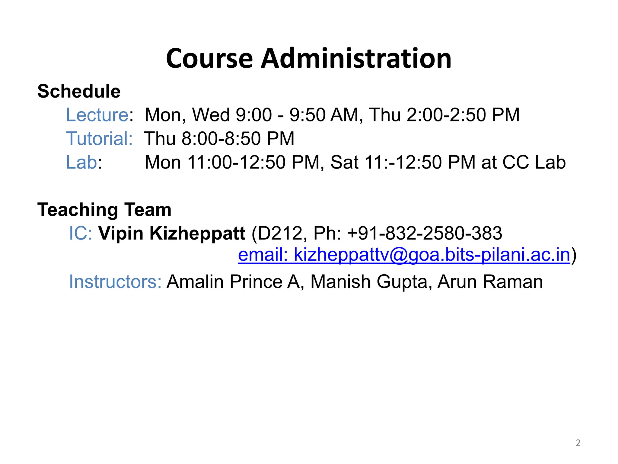
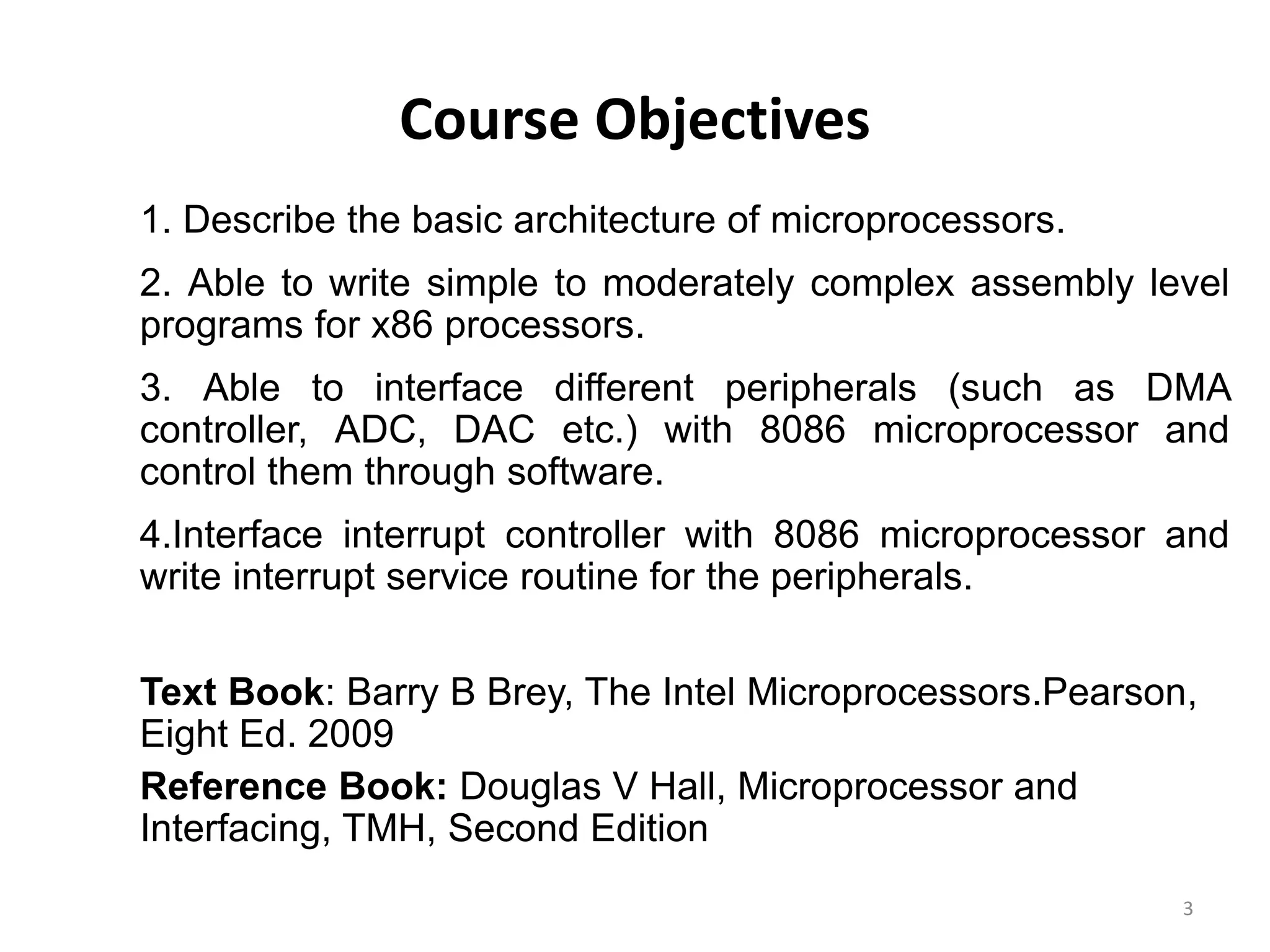
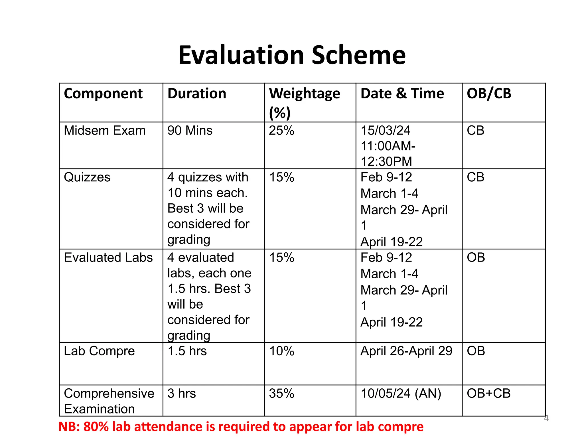
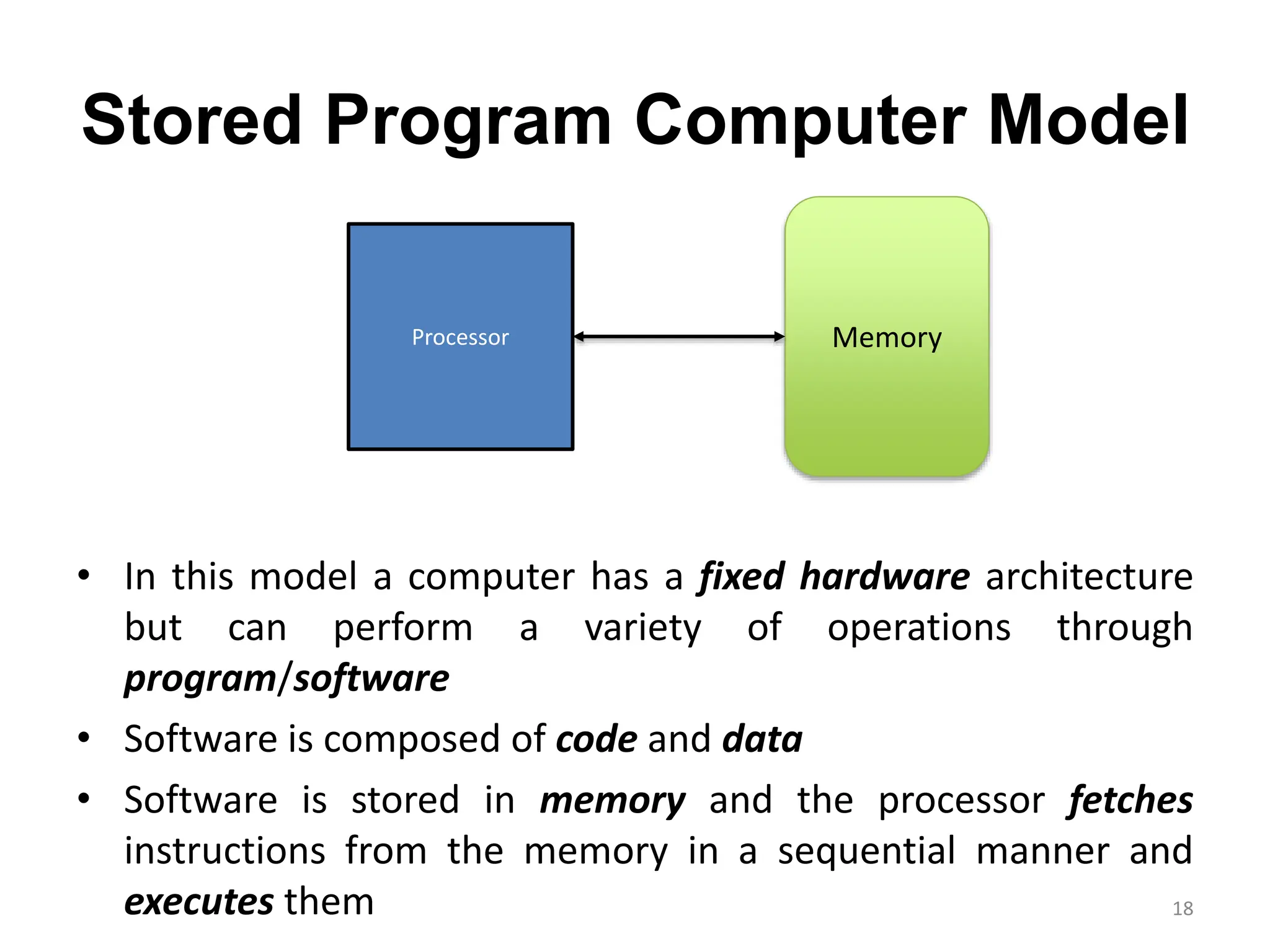
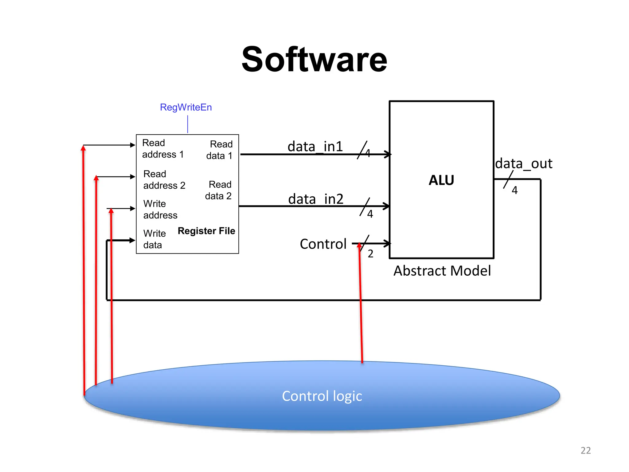
The document outlines a course on microprocessor programming and interfacing, covering key objectives such as basic microprocessor architecture, assembly programming for x86 processors, and peripheral interfacing. It includes details about the course schedule, evaluation scheme, textbooks, and lab attendance requirements. The teaching team comprises Vipin Kizheppatt as the instructor and several other supporting instructors.
![Memory Abstract Model
25
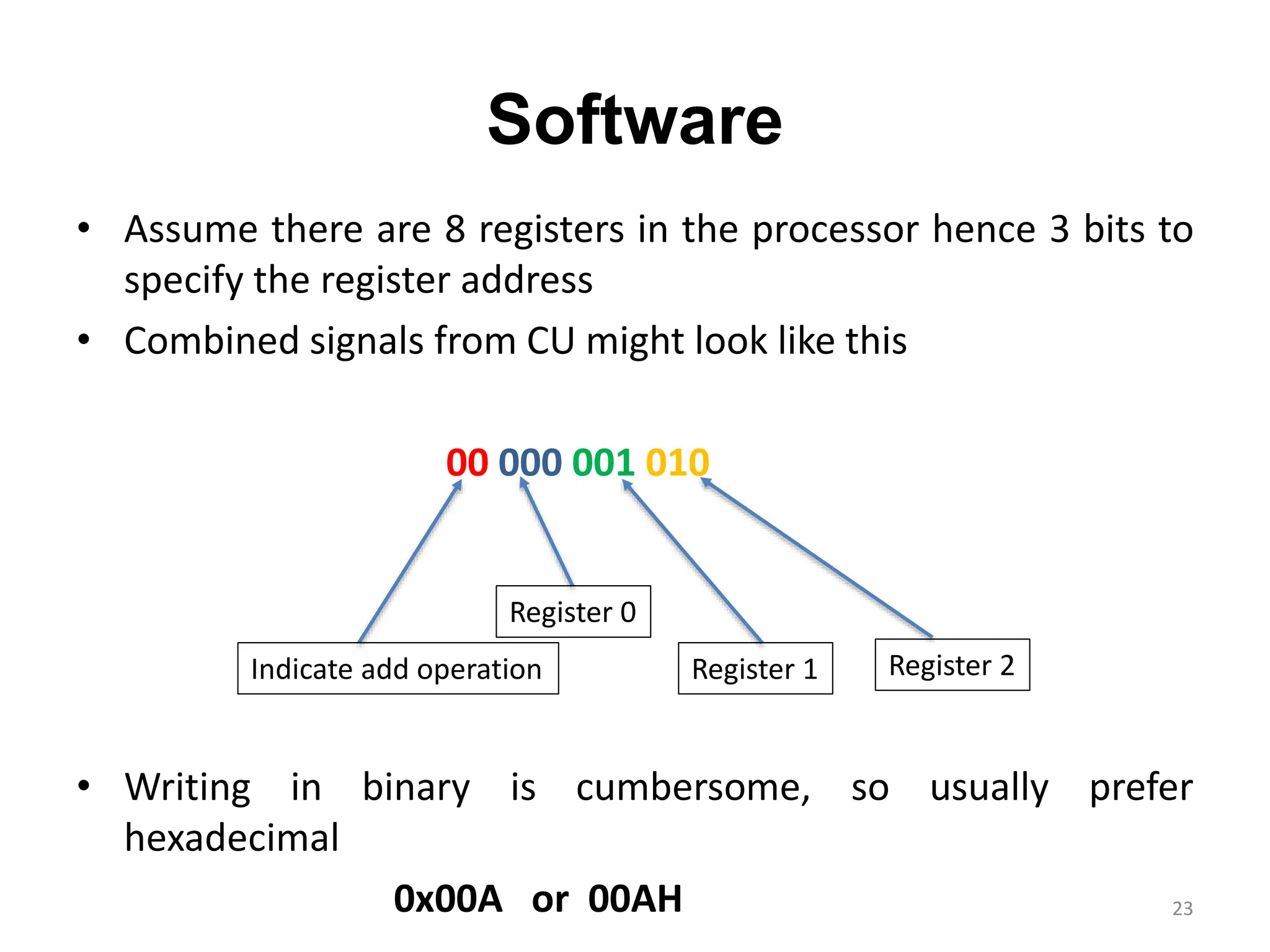
Memory
Address [a1:a0]
Data[3:0]
WE#
RE#](https://image.slidesharecdn.com/l1introduction-240424020759-7bde5ddc/75/Introduction-to-Microprocesso-programming-and-interfacing-pptx-25-2048.jpg)
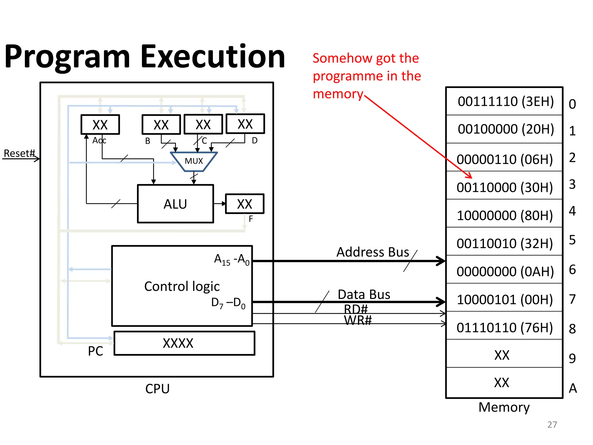
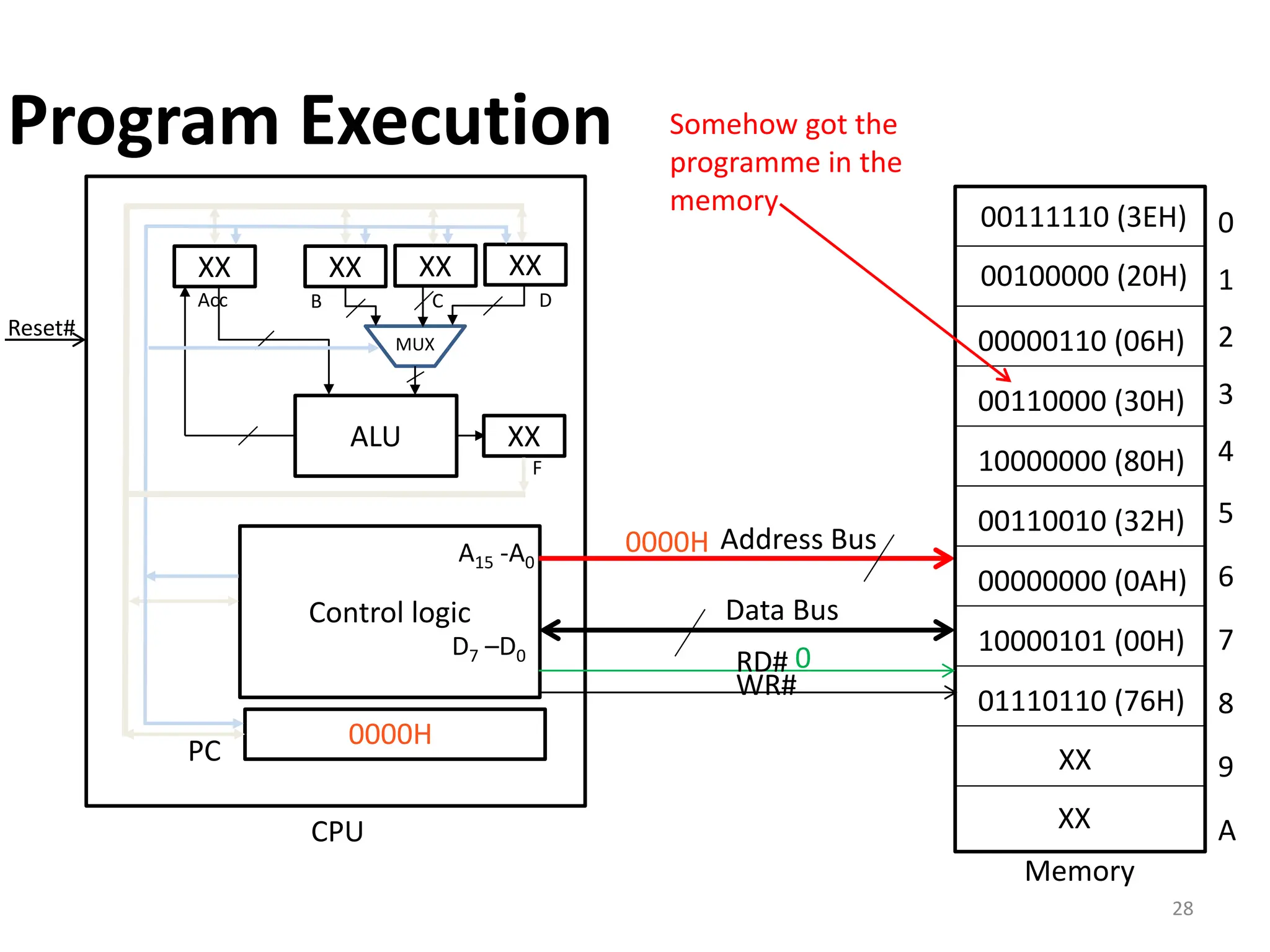
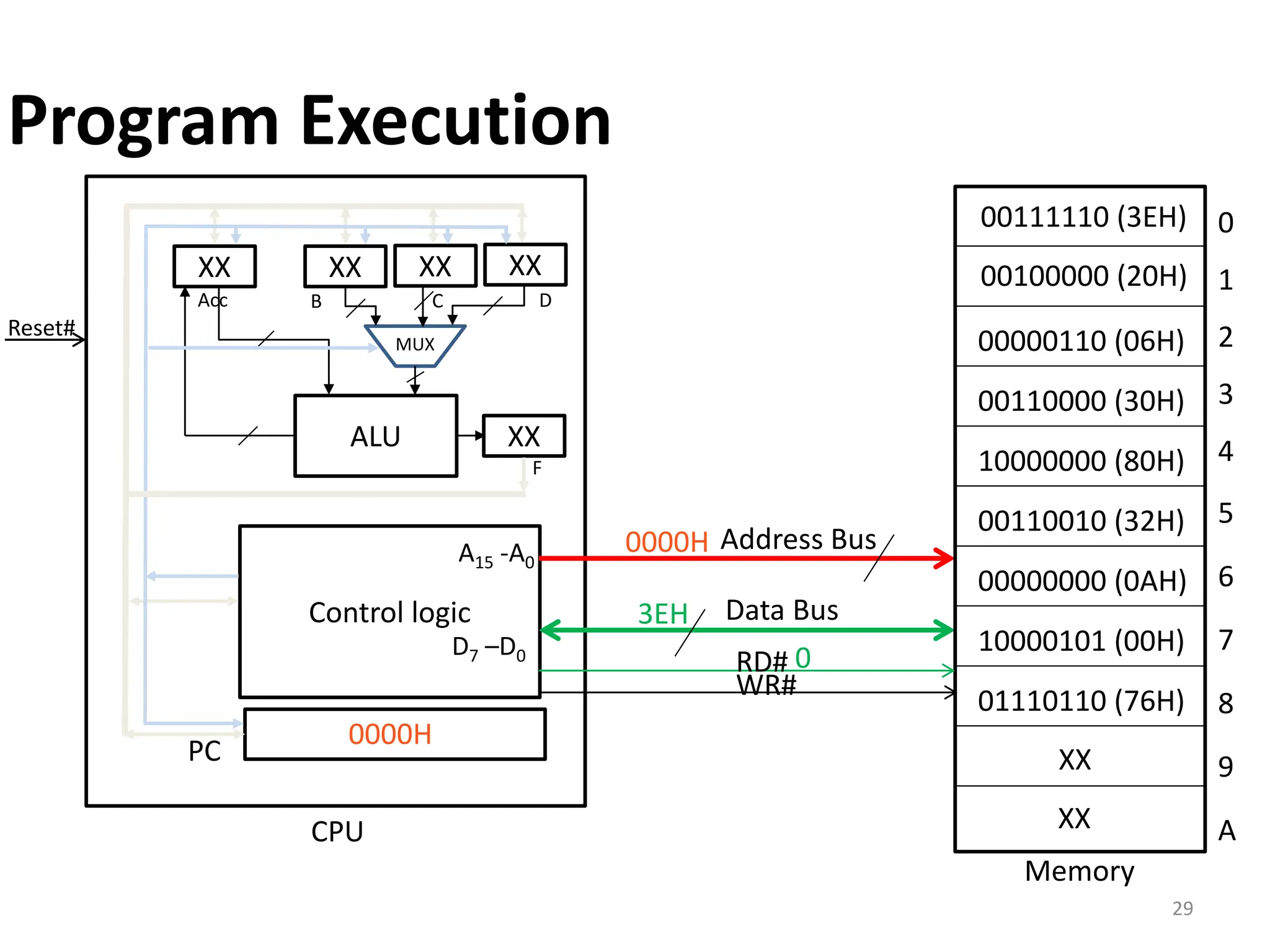
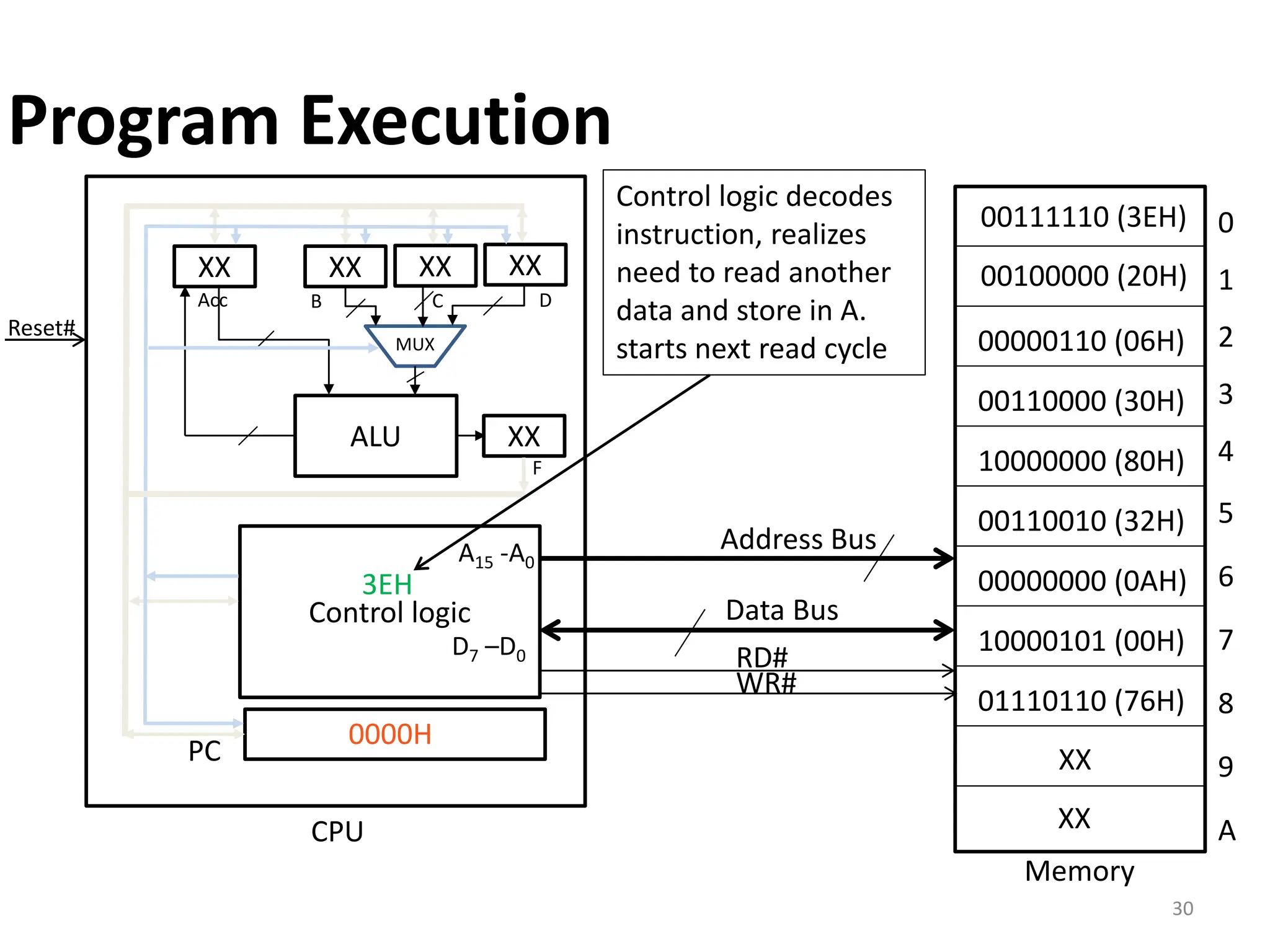
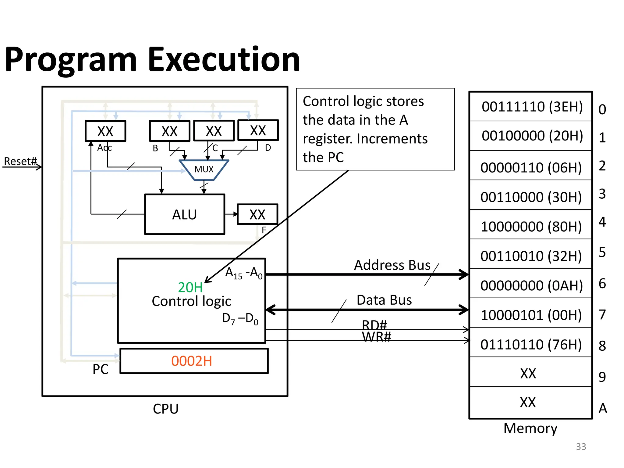
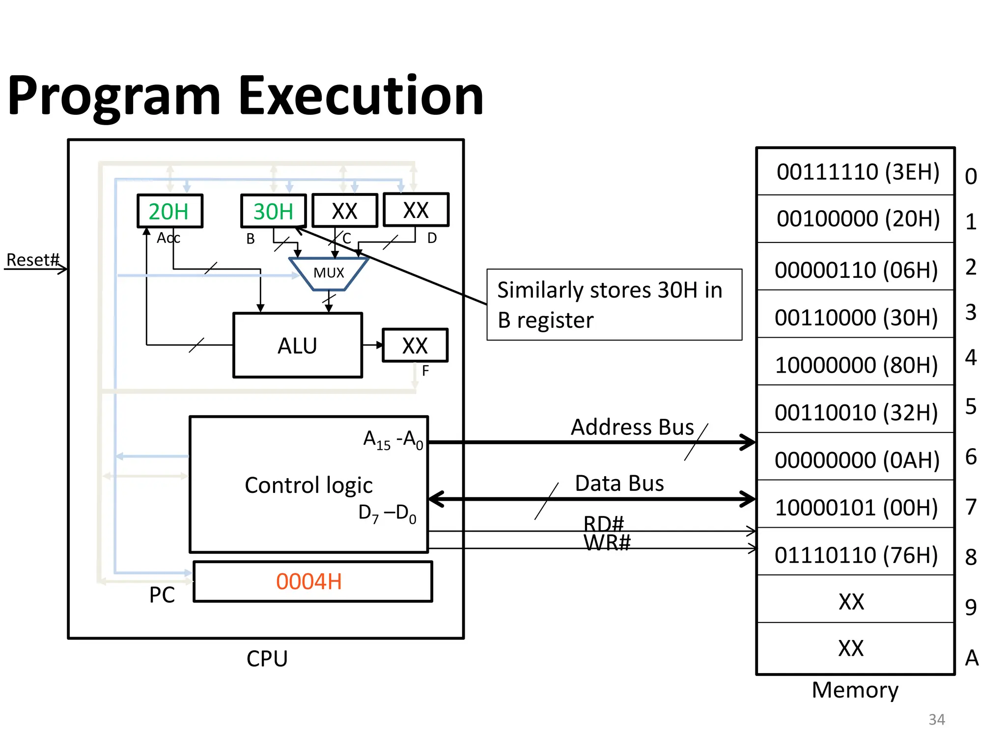
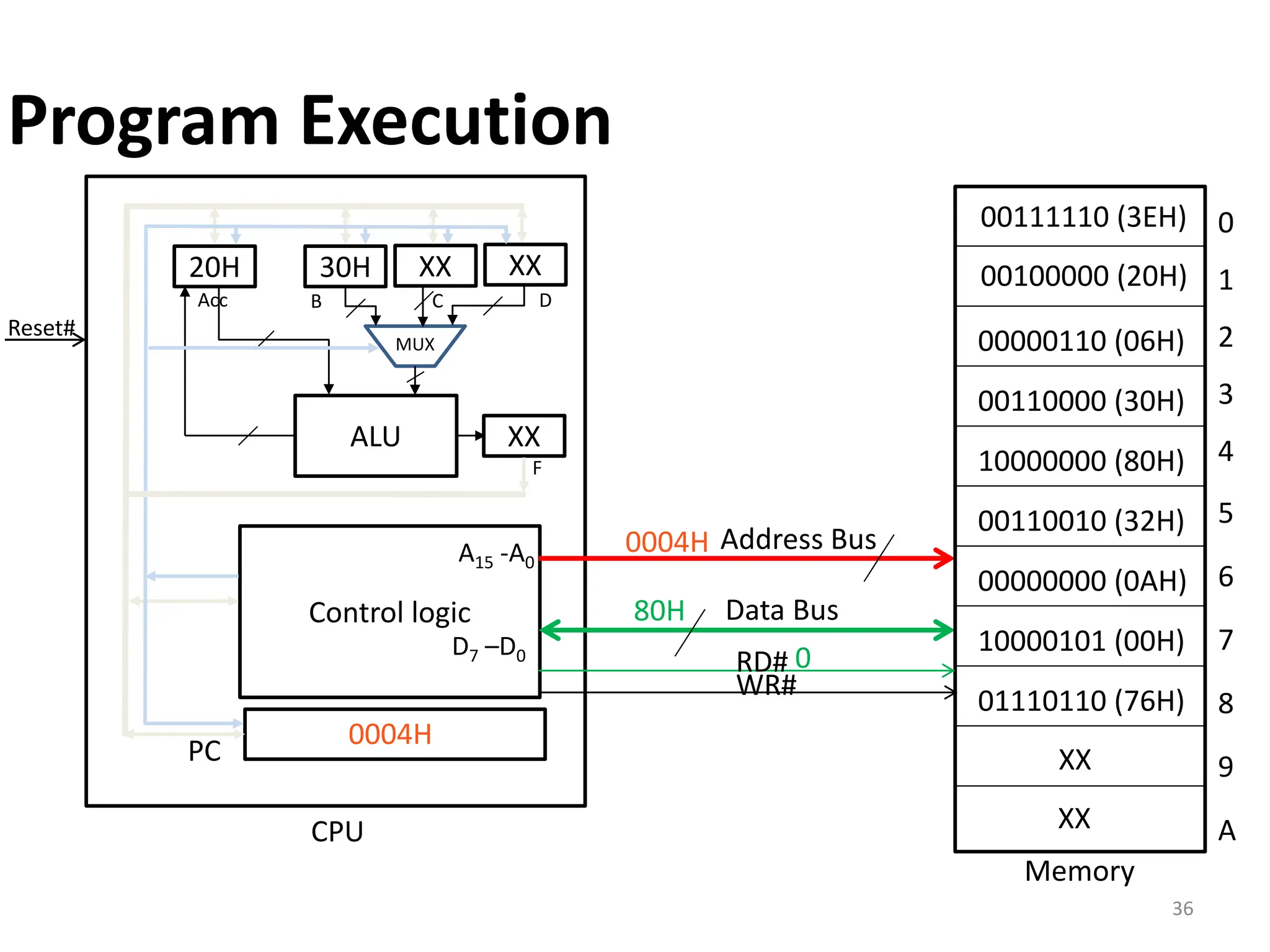
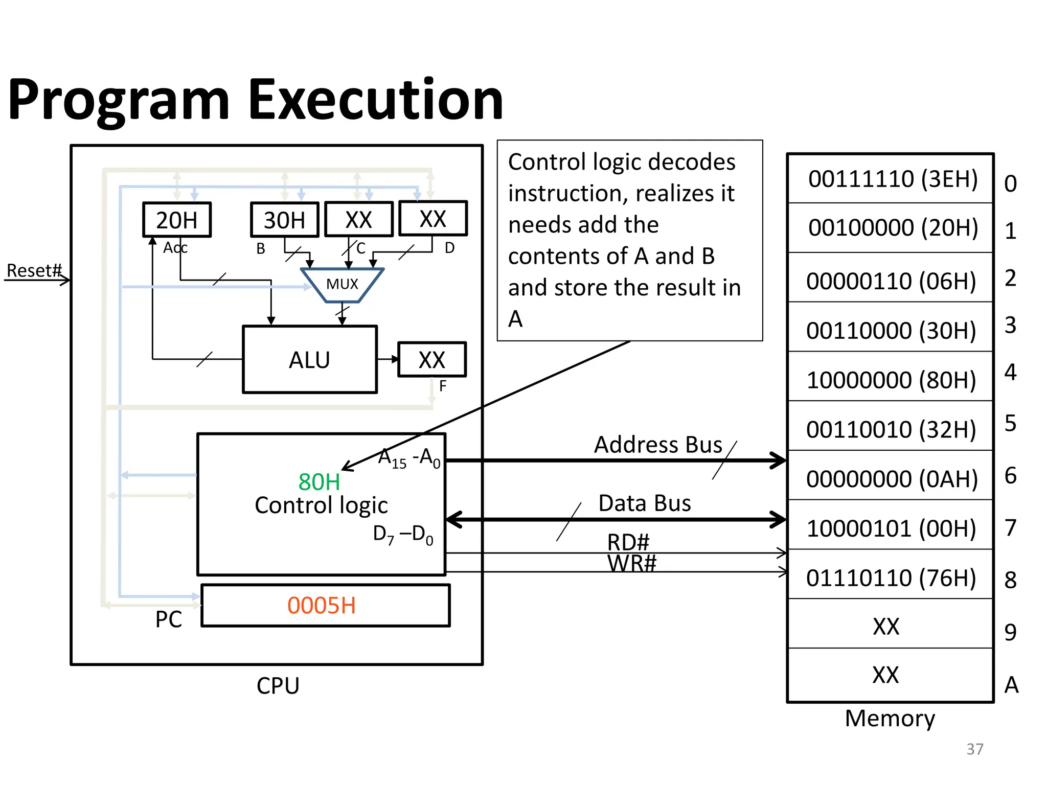
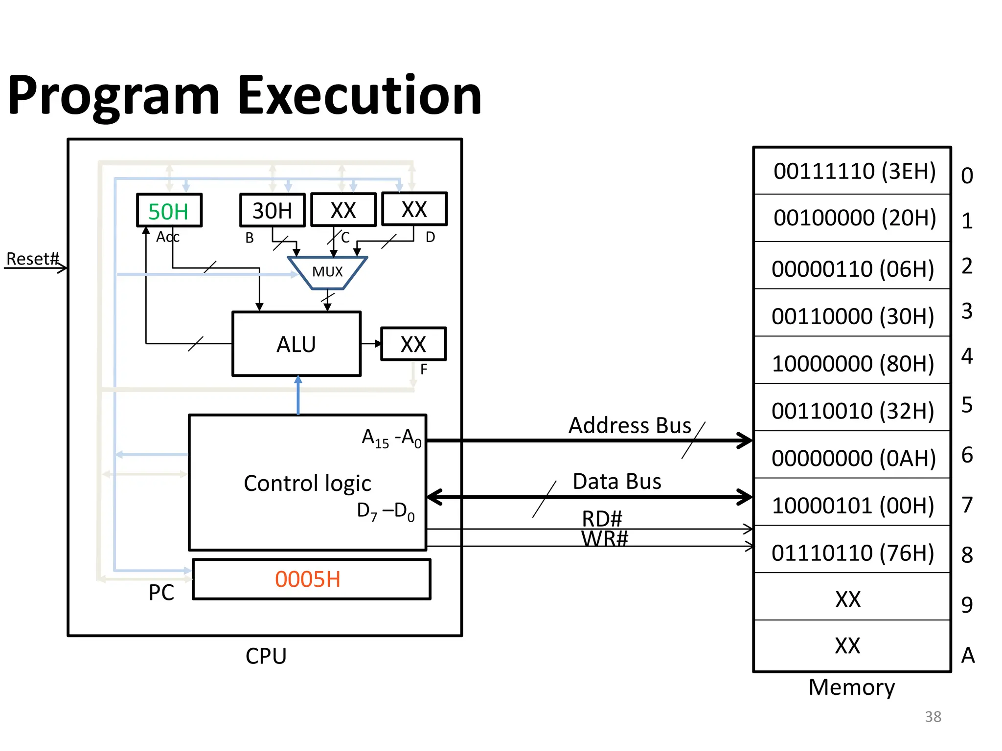
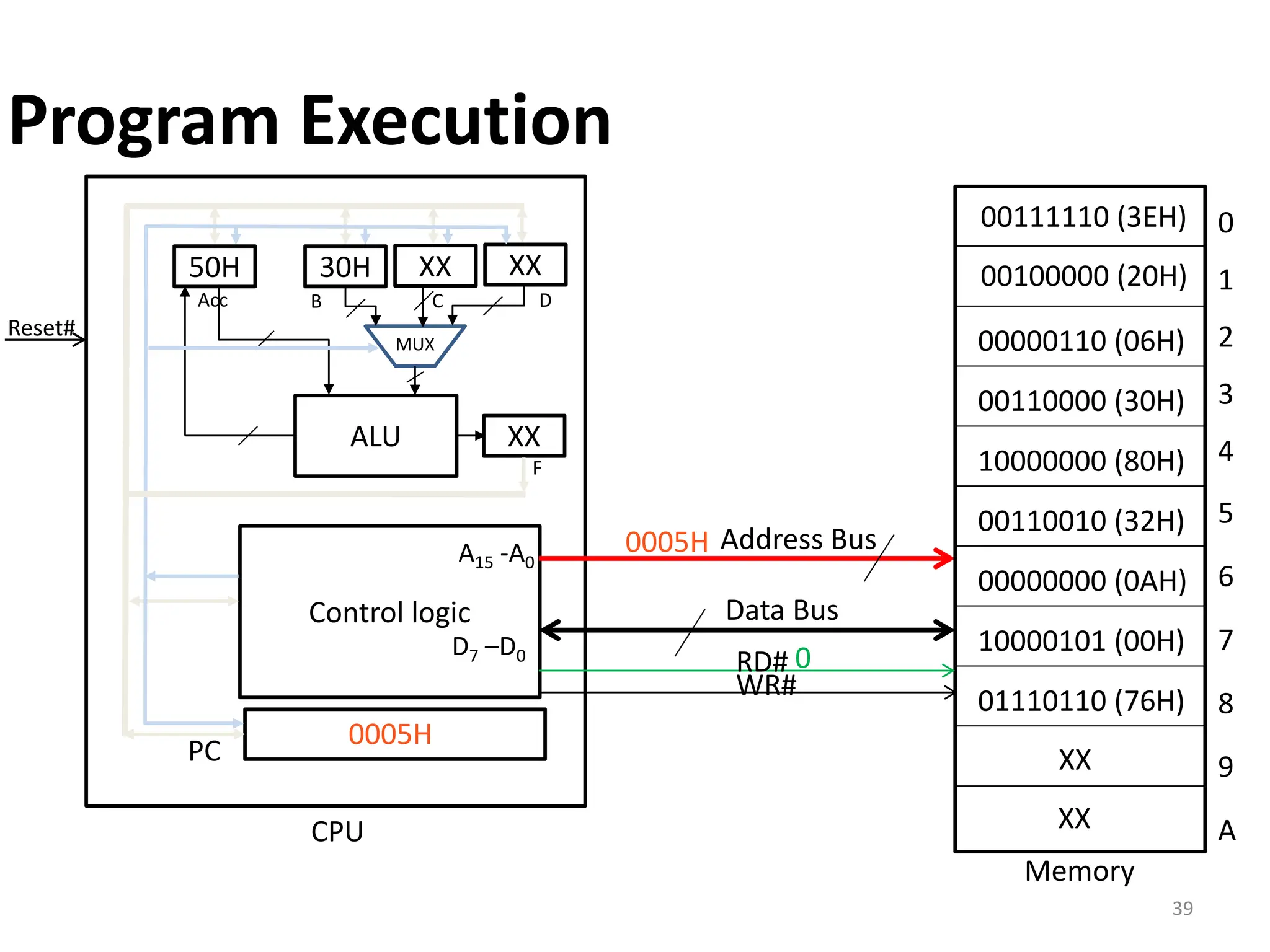
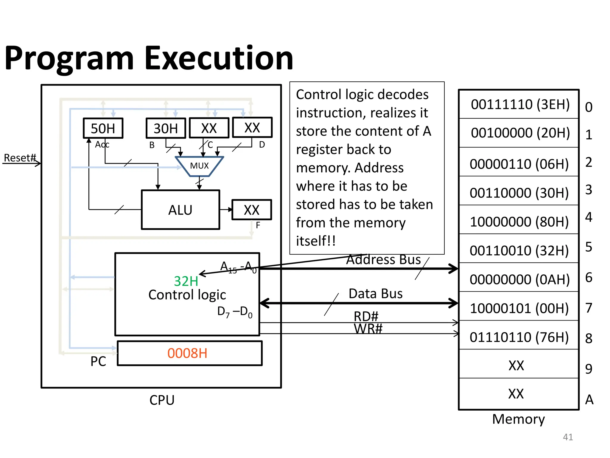
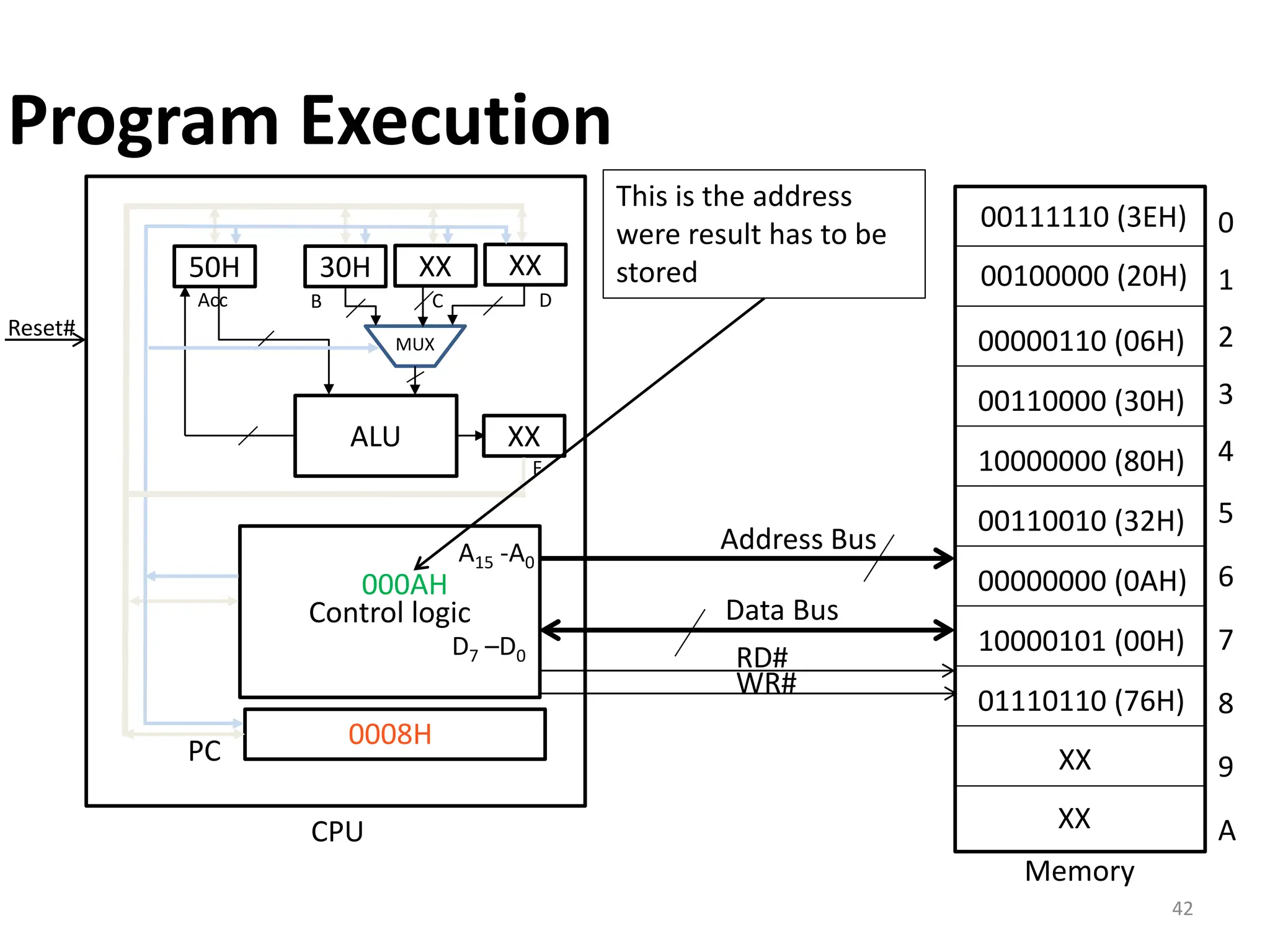
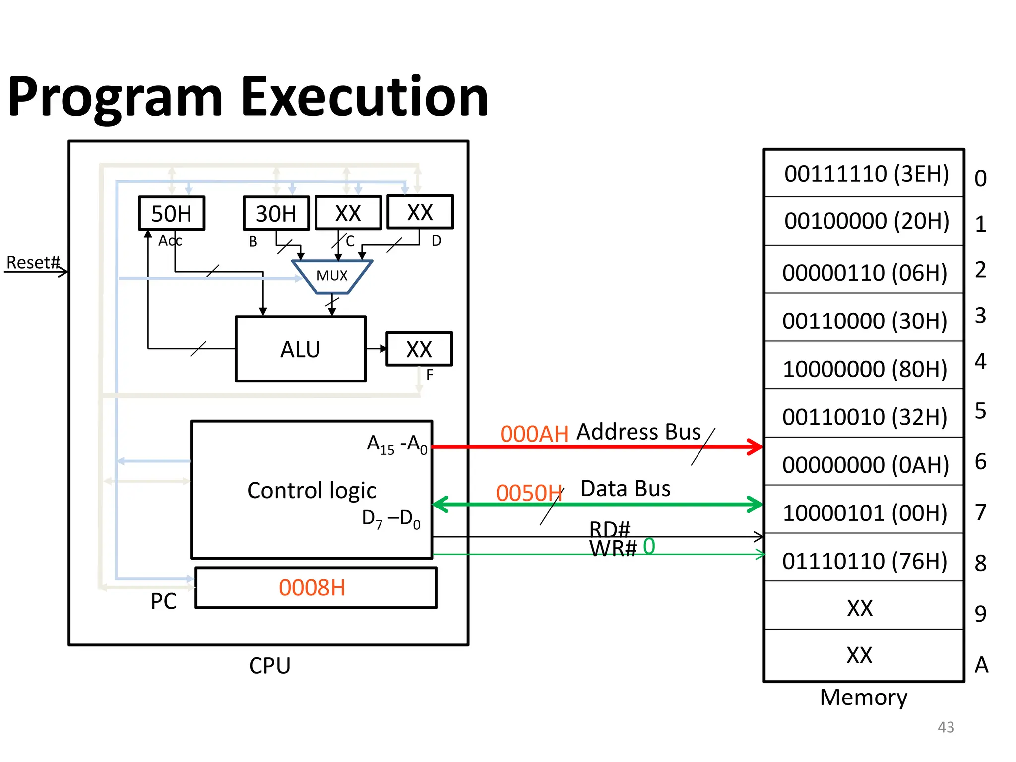
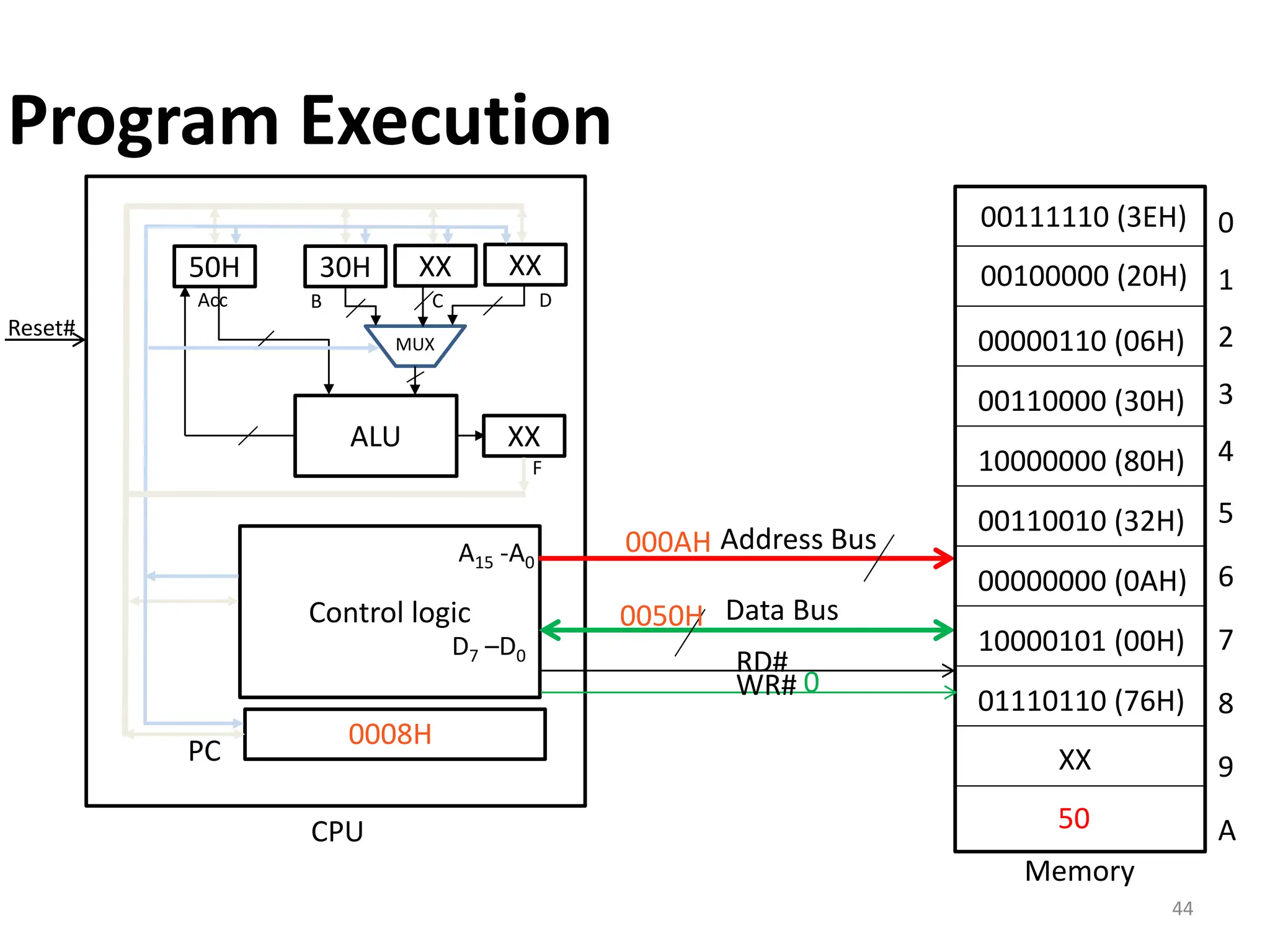
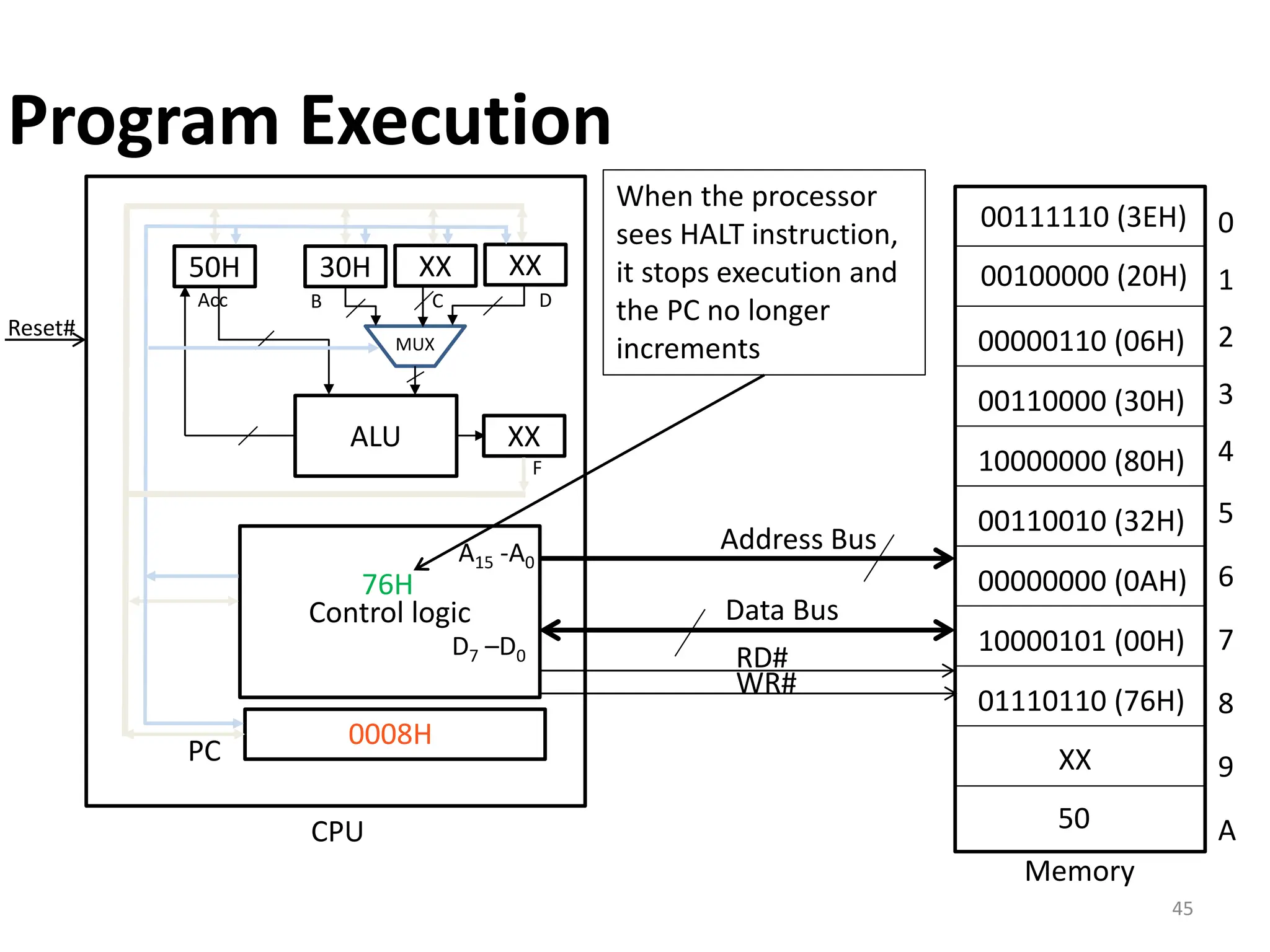
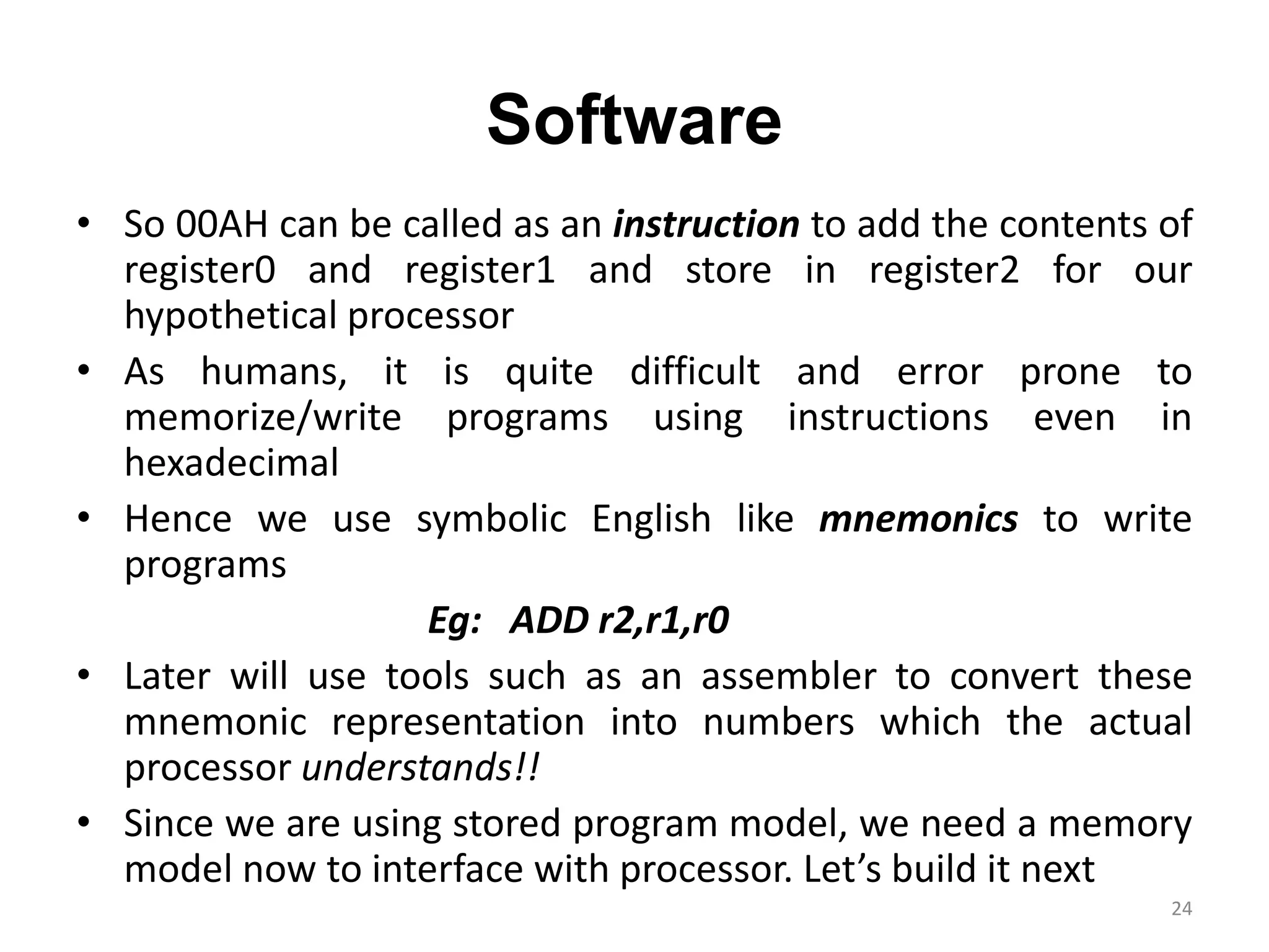
![Sample assembly program and
machine code
• Aim Add 20H and 30H and store the result in memory
location 000AH
• Assembly Code Hex Code
• MOV A,#20H 3E 20
• MOV B,#30H 06 30
• ADD A,B 80
• MOV [000AH],A 32 0A 00
• HLT 76
26](https://image.slidesharecdn.com/l1introduction-240424020759-7bde5ddc/75/Introduction-to-Microprocesso-programming-and-interfacing-pptx-26-2048.jpg)