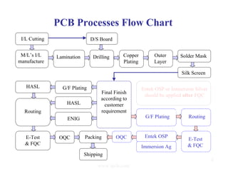
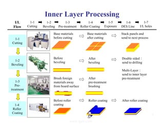
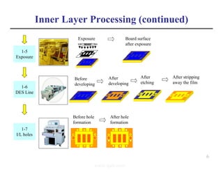
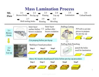
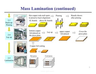
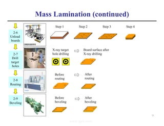
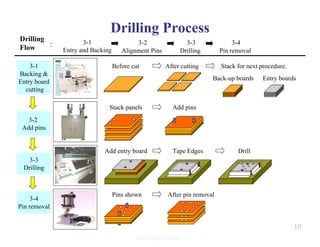
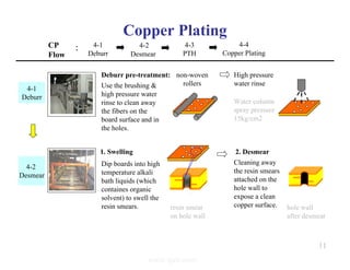
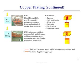
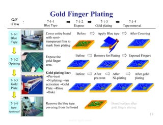
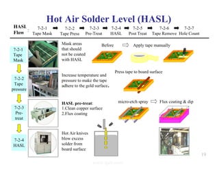
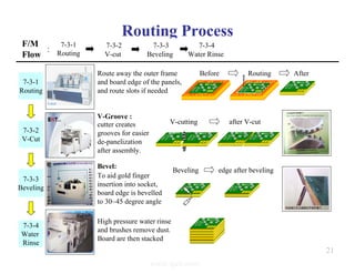
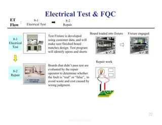
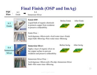
PCB Fabrication
Processes
Brief Introduction
www.ipcb.com
Contents
PCB Processes Flow Chart ……………………………..……… (001) 4
1. Inner Layer Processing ….…………………...………………… (002) 5
2. Mass Lamination ……………………..………………………… (032) 7
3. Drilling ……………………..……………………………….…. (058) 10
4. Copper Plating …….….……….………………………..……… (071) 11
5. Outer Layer Processing………………………………………… (102) 13
6. 1. Solder Mask ………………………………………………….… (123) 15
6. 2. Silk Screen …………………………………….……………..… (147) 17
7. 1. Gold Finger Plating ……….……………….…………………… (158) 18
7. 2. HASL ………….…………………………………………..…… (173) 20
7. 3. Routing …………….……………………………..………….… (190) 21
8. Electrical Test & FQC ………..………..……………………… (205) 22
www.ipcb.com
PCB Fabrication
Processes
Brief Introduction
3
www.ipcb.com
D/S Board
Lamination
ENIG
G/F Plating
HASL
Packing
Shipping
M/L’s I/L
manufacture
HASL
Final Finish
according to
customer
requirement
Drilling Copper
Plating
Outer
Layer
Solder Mask
Silk Screen
E-Test
& FQC
OQC Entek OSP
Immersion Ag
OQC
E-Test
& FQC
Routing
I/L Cutting
PCB Processes Flow Chart
4
Routing
G/F Plating
Entek OSP or Immersion Silver
should be applied after FQC
www.ipcb.com
Inner Layer Processing
Base materials
before cutting
Base materials
after cutting
Stack panels and
send to next process
Before
beveling
After
beveling
1-3
Pre-
treatment
Brush foreign
materials away
from board surface
After
pre-treatment
brushing
1-4
Roller
Coating
Before roller
coating
Roller coating After roller coating
Double sided:
send to drilling
Multi-Layer:
send to inner layer
pre-treatment
1-1
Cutting
1-2
Beveling
I/L
Flow
1-1
Cutting
1-2
Beveling
1-4
Roller Coating
1-5
Exposure
1-6
DES Line
1-7
I/L holes
1-3
Pre-treatment
5
www.ipcb.com
1-5
Exposure
Exposure Board surface
after exposure
1-6
DES Line
Before
developing
After
developing
After
etching
After stripping
away the film
1-7
I/L holes
Before hole
formation
After hole
formation
6
Inner Layer Processing (continued)
www.ipcb.com
Mass Lamination Process
2-1
Brown
Oxide
Inner layer
surface before
brown oxidation
Inner layer
surface after
brown oxidation
2-2
Pre
Lay-up
Cut prepreg before pre-layup
Above 8L boards should punch holes before pre-lay up procedure.
PrePreg Cutting
P/P roll is cut into
pieces to prepare
for pre-lay up
PrePreg Hole Punching
punch the holes
used for lamination
Step 1 Step 2 Step3
Step 2 Step3 Step4 Step5
Step 1
Multilayer board procedure:
7
ML
Flow
2-1
Brown Oxide
2-2
Pre-lay up
2-4
Lay up
2-5
Lamination
2-6
Unload boards
2-3
Pinning
:
2-8
Routing
2-9
Beveling
2-7
Drill tooling holes
www.ipcb.com
Mass Lamination (continued)
2-4
Lay up
Copper foil cutting
bottom copper
foil placed on
the press plate
Lay up upper copper
foil placed
Cover the
press plate
2-5
Lamination
Hot press Cool press
2-3
Stack-up
Pinning
4L boards above 8L boards
Hot copper rods melt spots
to preserve layer alignment.
Pinning Boards shown
after pinning
8
www.ipcb.com
Mass Lamination (continued)
2-7
Drill
target
holes
X-ray target
hole drilling
Board surface after
X-ray drilling
2-8
Routing
Before
routing
After
routing
Before
beveling
After
beveling
2-9
Beveling
Step 1 Step 2 Step 4
2-6
Unload
boards
Step 3
9
www.ipcb.com
Drilling Process
3-1
Backing &
Entry board
cutting
Before cut After cutting Stack for next procedure.
Back-up boards Entry boards
3-2
Add pins
Stack panels Add pins
3-3
Drilling
Add entry board Tape Edges Drill
3-4
Pin removal
Pins shown After pin removal
Drilling
Flow
3-1
Entry and Backing
3-2
Alignment Pins
3-4
Pin removal
3-3
Drilling
:
10
www.ipcb.com
Copper Plating
4-1
Deburr
Deburr pre-treatment: non-woven
rollers
High pressure
water rinse
Water column
spray pressure
15kg/cm2
4-2
Desmear
1. Swelling
Dip boards into high
temperature alkali
bath liquids (which
containes organic
solvent) to swell the
resin smears.
Use the brushing &
high pressure water
rinse to clean away
the fibers on the
board surface and in
the holes.
2. Desmear
Cleaning away
the resin smears
attached on the
hole wall to
expose a clean
copper surface. hole wall
after desmear
resin smear
on hole wall
CP
Flow
4-1
Deburr
4-2
Desmear
4-4
Copper Plating
4-3
PTH
:
11
www.ipcb.com
Copper Plating (continued)
4-3
PTH
PTH:
Plated Through Holes
provide conductive
connections between
layers, and mechanical
support for components
PTH process:
→ Desmear
→ Hole conditioning
→ Micro-etch
→ Activation
→ Acceleration
→ Electroless copper
“ ” indicates Electroless copper plating on base copper and hole wall
4-4
Plating
PTH plating must establish
minimum hole wall thickness,
and increase surface copper
thickness to meet specification
or customer requirement.
“ ” indicates the plated copper layer
12
www.ipcb.com
Outer Layer Processing
5-1
Pre-
treat
Pumice Line:
Clean foreign material
from board surface and
roughen board surface
to increase adhesion to
dry film
Board surface
before pre-treat
Board surface
after pre-treat
5-2
Etch
Resist
Dry film:
consists of PE film,
photopolymer film
resist and PET film
PET
PE
Heat and sentering
press to apply the
dry film on the
board surface.
Laminator:
O/L
Flow
5-1
Pre-treatment
5-2
Etch Resist
5-4
DES Line
5-3
Exposure
:
13
www.ipcb.com
Outer Layers (continued)
5-3
Image
Exposure
Exposure:
Blue material is light-
sensitive, so UV energy
will cause a chemical
reaction to “cure” the
areas that are exposed by
the image.
clean room
5-4
DES Line
Before
developing
After
developing
After
etching
After stripping
away the film
14
www.ipcb.com
Solder Mask Process
6-1-1
Pre-
treat
Pumice Line:
Clean foreign material
and roughen the board
surface to increase
solder mask adhesion
Before pre-treat After pre-treat
6-1-2
Print
Printing:
Apply photoimagible mask
on board surface to protect
circuitry, prevent copper
surface oxidation and act
as solder resist
6-1-3
Pre-
cure
Pre-curing:
Partially remove
solvent so surface
is not tacky
S/M
Flow
6-1-1
Pre-treatment
6-1-2
Printing
6-1-4
Developing
6-1-3
Pre-curing
: 6-1-5
Post-Curing
15
Before mask After mask
www.ipcb.com
Solder Mask Process
6-1-5
Post
curing
Post Cure :
Final cure to increase surface
hardness and resist soldering
(board appears same
as in previous step)
16
6-1-4
Develop
Remove the solder mask
which wasn’t exposed to
UV curing
Developing: Before developing After developing
www.ipcb.com
Silk Screen Process
6-2-1
Screen
printing
Legend:
Text and/or numbers printed on the final board surface using
non-conductive ink. Commonly used to identify components
(and orientation or polarity), and identifying board part
number and revision level.
煙台PCB
IC 111
R 168
煙台PCB
IC 111
R 168
R28
U37
6-2-2
Post
curing
Legend baking oven:
The ink used for silk screen printing contains hardening
ingredients that are activated thermally, so it is cured at
high temperature. This is called “Polymerization” or a
“crosslinkage reaction”
S/S
Flow
6-2-1
Screen printing
6-2-2
Post curing
:
17
www.ipcb.com
Gold Finger Plating
7-1-1
Blue
Tape
Cover entire board
with semi-
transparent film to
mask from plating
Before
煙台PCB
IC111
Apply Blue tape After Covering
1
1
1
煙台PCB
IC111
7-1-2
Opening
Expose the
gold finger
area.
Before
煙台 PCB
IC 111
Remove for Plating
I
C
1
1
1
煙台 PCB
IC 111
Exposed Fingers
煙台 PCB
IC 111
7-1-3
Gold
Plate
Gold plating line:
→Pre-treat
→Ni plating →Au
activation →Gold
Plate →Rinse
→Bake
Before After
pre-treat
After
Ni-plating
After gold
plating
煙台 PCB
IC 111
煙台 PCB
IC 111
煙台 PCB
IC 111
煙台 PCB
IC 111
7-1-4
tape
removal
Remove the blue tape
covering from the board
Board surface after
gold finger plating
煙台 PCB
IC 111
G/F
Flow
7-1-1
Blue Tape
7-1-2
Expose
7-1-4
Tape removal
7-1-3
Gold plating
:
18
www.ipcb.com
Hot Air Solder Level (HASL)
7-2-1
Tape
Mask
Mask areas
that should
not be coated
with HASL
Before
煙台 PCB
IC 111
Apply tape manually
煙台 PCB
IC 111
7-2-2
Tape
pressure
Increase temperature and
pressure to make the tape
adhere to the gold surface。
煙台 PCB
IC 111
Press tape to board surface
7-2-3
Pre-
treat
HASL pre-treat:
1.Clean copper surface
2.Flux coating
煙台 PCB
IC 111
micro-etch spray Flux coating & dip
7-2-4
HASL
Hot Air knives
blow excess
solder from
board surface
煙台 PCB
IC 111
HASL
Flow
7-2-1
Tape Mask
7-2-2
Tape Press
7-2-4
HASL
7-2-3
Pre-Treat
:
7-2-5
Post Treat
7-2-7
Hole Count
7-2-6
Tape Remove
19
www.ipcb.com
HASL process (continued)
7-2-5
Post
Treat
Post treatment
cleaning line
brushes debris
from the board
surface
煙台 PCB
IC 111
7-2-6
Tape
Removal
Solder board
surface after
removing tape
煙台 PCB
IC 111
7-2-7
Hole
Count
Hole Counter :
Uses light to perform
automatic checking for
correct hole count, will
detect missed drilling
and plugged holes
煙台 PCB
IC 111
20
www.ipcb.com
Routing Process
7-3-1
Routing
Route away the outer frame
and board edge of the panels,
and route slots if needed
Before
煙台 PCB
IC 111
Routing
煙台 PCB
IC 111
After
煙台 PCB
IC 111
7-3-2
V-Cut
V-Groove :
cutter creates
grooves for easier
de-panelization
after assembly.
煙台 PCB
IC 111
煙台 PCB
IC 111
V-cutting after V-cut
7-3-3
Beveling
Bevel:
To aid gold finger
insertion into socket,
board edge is bevelled
to 30~45 degree angle
煙台 PCB
IC 111
煙台 PCB
IC 111
Beveling edge after beveling
7-3-4
Water
Rinse
High pressure water rinse
and brushes remove dust.
Board are then stacked
煙台 PCB
IC 111
煙台 PCB
IC 111
煙台 PCB
IC 111
煙台 PCB
IC 111
煙台 PCB
IC 111
煙台 PCB
IC 111
煙台 PCB
IC 111
7-3-1
Routing
7-3-2
V-cut
7-3-4
Water Rinse
7-3-3
Beveling
:
F/M
Flow
21
www.ipcb.com
Electrical Test & FQC
8-1
Electrical
Test
Test Fixture is developed
using customer data, and will
make sure finished board
matches design. Test program
will identify opens and shorts
Board loaded into fixture Fixture engaged
8-2
Repair
煙台 PCB
IC 111
Boards that didn’t pass test are
evaluated by the repair
operator to determine whether
the fault is “real” or “false”, to
avoid waste and cost caused by
wrong judgment.
Repair work
ET
Flow
8-1
Electrical Test
8-2
Repair
:
22
www.ipcb.com
Final Finish (OSP and ImAg)
8-3
Entek
Entek OSP:
Liquid bath of organic chemicals
to protects copper from oxidation
to preserve solderability
煙台 PCB
IC 111
煙台 PCB
IC 111
Before Entek After Entek
Entek Flow:
Acid degrease→Micro-etch→Acid water rinse→Entek
major bath→Blowing→Pure water rinse→Blowing
8-4
Immersion
Silver
Immersion Silver:
Apply a layer of organic silver on
the copper surface to prevent
oxidation and preserve solderability
Before ImAg
煙台 PCB
IC 111
After ImAg
煙台 PCB
IC 111
Immersion Silver Flow :
Acid degrease→Micro-etch→Pre-dip→Immersion Silver
Bath→Hot water rinse→Blowing
FQC
Flow
8-3
Entek
8-4
Immersion Silver
:
23
www.ipcb.com

Pcb fabrication-process

  • 1.
  • 2.
    Contents PCB Processes FlowChart ……………………………..……… (001) 4 1. Inner Layer Processing ….…………………...………………… (002) 5 2. Mass Lamination ……………………..………………………… (032) 7 3. Drilling ……………………..……………………………….…. (058) 10 4. Copper Plating …….….……….………………………..……… (071) 11 5. Outer Layer Processing………………………………………… (102) 13 6. 1. Solder Mask ………………………………………………….… (123) 15 6. 2. Silk Screen …………………………………….……………..… (147) 17 7. 1. Gold Finger Plating ……….……………….…………………… (158) 18 7. 2. HASL ………….…………………………………………..…… (173) 20 7. 3. Routing …………….……………………………..………….… (190) 21 8. Electrical Test & FQC ………..………..……………………… (205) 22 www.ipcb.com
  • 3.
  • 4.
    D/S Board Lamination ENIG G/F Plating HASL Packing Shipping M/L’sI/L manufacture HASL Final Finish according to customer requirement Drilling Copper Plating Outer Layer Solder Mask Silk Screen E-Test & FQC OQC Entek OSP Immersion Ag OQC E-Test & FQC Routing I/L Cutting PCB Processes Flow Chart 4 Routing G/F Plating Entek OSP or Immersion Silver should be applied after FQC www.ipcb.com
  • 5.
    Inner Layer Processing Basematerials before cutting Base materials after cutting Stack panels and send to next process Before beveling After beveling 1-3 Pre- treatment Brush foreign materials away from board surface After pre-treatment brushing 1-4 Roller Coating Before roller coating Roller coating After roller coating Double sided: send to drilling Multi-Layer: send to inner layer pre-treatment 1-1 Cutting 1-2 Beveling I/L Flow 1-1 Cutting 1-2 Beveling 1-4 Roller Coating 1-5 Exposure 1-6 DES Line 1-7 I/L holes 1-3 Pre-treatment 5 www.ipcb.com
  • 6.
    1-5 Exposure Exposure Board surface afterexposure 1-6 DES Line Before developing After developing After etching After stripping away the film 1-7 I/L holes Before hole formation After hole formation 6 Inner Layer Processing (continued) www.ipcb.com
  • 7.
    Mass Lamination Process 2-1 Brown Oxide Innerlayer surface before brown oxidation Inner layer surface after brown oxidation 2-2 Pre Lay-up Cut prepreg before pre-layup Above 8L boards should punch holes before pre-lay up procedure. PrePreg Cutting P/P roll is cut into pieces to prepare for pre-lay up PrePreg Hole Punching punch the holes used for lamination Step 1 Step 2 Step3 Step 2 Step3 Step4 Step5 Step 1 Multilayer board procedure: 7 ML Flow 2-1 Brown Oxide 2-2 Pre-lay up 2-4 Lay up 2-5 Lamination 2-6 Unload boards 2-3 Pinning : 2-8 Routing 2-9 Beveling 2-7 Drill tooling holes www.ipcb.com
  • 8.
    Mass Lamination (continued) 2-4 Layup Copper foil cutting bottom copper foil placed on the press plate Lay up upper copper foil placed Cover the press plate 2-5 Lamination Hot press Cool press 2-3 Stack-up Pinning 4L boards above 8L boards Hot copper rods melt spots to preserve layer alignment. Pinning Boards shown after pinning 8 www.ipcb.com
  • 9.
    Mass Lamination (continued) 2-7 Drill target holes X-raytarget hole drilling Board surface after X-ray drilling 2-8 Routing Before routing After routing Before beveling After beveling 2-9 Beveling Step 1 Step 2 Step 4 2-6 Unload boards Step 3 9 www.ipcb.com
  • 10.
    Drilling Process 3-1 Backing & Entryboard cutting Before cut After cutting Stack for next procedure. Back-up boards Entry boards 3-2 Add pins Stack panels Add pins 3-3 Drilling Add entry board Tape Edges Drill 3-4 Pin removal Pins shown After pin removal Drilling Flow 3-1 Entry and Backing 3-2 Alignment Pins 3-4 Pin removal 3-3 Drilling : 10 www.ipcb.com
  • 11.
    Copper Plating 4-1 Deburr Deburr pre-treatment:non-woven rollers High pressure water rinse Water column spray pressure 15kg/cm2 4-2 Desmear 1. Swelling Dip boards into high temperature alkali bath liquids (which containes organic solvent) to swell the resin smears. Use the brushing & high pressure water rinse to clean away the fibers on the board surface and in the holes. 2. Desmear Cleaning away the resin smears attached on the hole wall to expose a clean copper surface. hole wall after desmear resin smear on hole wall CP Flow 4-1 Deburr 4-2 Desmear 4-4 Copper Plating 4-3 PTH : 11 www.ipcb.com
  • 12.
    Copper Plating (continued) 4-3 PTH PTH: PlatedThrough Holes provide conductive connections between layers, and mechanical support for components PTH process: → Desmear → Hole conditioning → Micro-etch → Activation → Acceleration → Electroless copper “ ” indicates Electroless copper plating on base copper and hole wall 4-4 Plating PTH plating must establish minimum hole wall thickness, and increase surface copper thickness to meet specification or customer requirement. “ ” indicates the plated copper layer 12 www.ipcb.com
  • 13.
    Outer Layer Processing 5-1 Pre- treat PumiceLine: Clean foreign material from board surface and roughen board surface to increase adhesion to dry film Board surface before pre-treat Board surface after pre-treat 5-2 Etch Resist Dry film: consists of PE film, photopolymer film resist and PET film PET PE Heat and sentering press to apply the dry film on the board surface. Laminator: O/L Flow 5-1 Pre-treatment 5-2 Etch Resist 5-4 DES Line 5-3 Exposure : 13 www.ipcb.com
  • 14.
    Outer Layers (continued) 5-3 Image Exposure Exposure: Bluematerial is light- sensitive, so UV energy will cause a chemical reaction to “cure” the areas that are exposed by the image. clean room 5-4 DES Line Before developing After developing After etching After stripping away the film 14 www.ipcb.com
  • 15.
    Solder Mask Process 6-1-1 Pre- treat PumiceLine: Clean foreign material and roughen the board surface to increase solder mask adhesion Before pre-treat After pre-treat 6-1-2 Print Printing: Apply photoimagible mask on board surface to protect circuitry, prevent copper surface oxidation and act as solder resist 6-1-3 Pre- cure Pre-curing: Partially remove solvent so surface is not tacky S/M Flow 6-1-1 Pre-treatment 6-1-2 Printing 6-1-4 Developing 6-1-3 Pre-curing : 6-1-5 Post-Curing 15 Before mask After mask www.ipcb.com
  • 16.
    Solder Mask Process 6-1-5 Post curing PostCure : Final cure to increase surface hardness and resist soldering (board appears same as in previous step) 16 6-1-4 Develop Remove the solder mask which wasn’t exposed to UV curing Developing: Before developing After developing www.ipcb.com
  • 17.
    Silk Screen Process 6-2-1 Screen printing Legend: Textand/or numbers printed on the final board surface using non-conductive ink. Commonly used to identify components (and orientation or polarity), and identifying board part number and revision level. 煙台PCB IC 111 R 168 煙台PCB IC 111 R 168 R28 U37 6-2-2 Post curing Legend baking oven: The ink used for silk screen printing contains hardening ingredients that are activated thermally, so it is cured at high temperature. This is called “Polymerization” or a “crosslinkage reaction” S/S Flow 6-2-1 Screen printing 6-2-2 Post curing : 17 www.ipcb.com
  • 18.
    Gold Finger Plating 7-1-1 Blue Tape Coverentire board with semi- transparent film to mask from plating Before 煙台PCB IC111 Apply Blue tape After Covering 1 1 1 煙台PCB IC111 7-1-2 Opening Expose the gold finger area. Before 煙台 PCB IC 111 Remove for Plating I C 1 1 1 煙台 PCB IC 111 Exposed Fingers 煙台 PCB IC 111 7-1-3 Gold Plate Gold plating line: →Pre-treat →Ni plating →Au activation →Gold Plate →Rinse →Bake Before After pre-treat After Ni-plating After gold plating 煙台 PCB IC 111 煙台 PCB IC 111 煙台 PCB IC 111 煙台 PCB IC 111 7-1-4 tape removal Remove the blue tape covering from the board Board surface after gold finger plating 煙台 PCB IC 111 G/F Flow 7-1-1 Blue Tape 7-1-2 Expose 7-1-4 Tape removal 7-1-3 Gold plating : 18 www.ipcb.com
  • 19.
    Hot Air SolderLevel (HASL) 7-2-1 Tape Mask Mask areas that should not be coated with HASL Before 煙台 PCB IC 111 Apply tape manually 煙台 PCB IC 111 7-2-2 Tape pressure Increase temperature and pressure to make the tape adhere to the gold surface。 煙台 PCB IC 111 Press tape to board surface 7-2-3 Pre- treat HASL pre-treat: 1.Clean copper surface 2.Flux coating 煙台 PCB IC 111 micro-etch spray Flux coating & dip 7-2-4 HASL Hot Air knives blow excess solder from board surface 煙台 PCB IC 111 HASL Flow 7-2-1 Tape Mask 7-2-2 Tape Press 7-2-4 HASL 7-2-3 Pre-Treat : 7-2-5 Post Treat 7-2-7 Hole Count 7-2-6 Tape Remove 19 www.ipcb.com
  • 20.
    HASL process (continued) 7-2-5 Post Treat Posttreatment cleaning line brushes debris from the board surface 煙台 PCB IC 111 7-2-6 Tape Removal Solder board surface after removing tape 煙台 PCB IC 111 7-2-7 Hole Count Hole Counter : Uses light to perform automatic checking for correct hole count, will detect missed drilling and plugged holes 煙台 PCB IC 111 20 www.ipcb.com
  • 21.
    Routing Process 7-3-1 Routing Route awaythe outer frame and board edge of the panels, and route slots if needed Before 煙台 PCB IC 111 Routing 煙台 PCB IC 111 After 煙台 PCB IC 111 7-3-2 V-Cut V-Groove : cutter creates grooves for easier de-panelization after assembly. 煙台 PCB IC 111 煙台 PCB IC 111 V-cutting after V-cut 7-3-3 Beveling Bevel: To aid gold finger insertion into socket, board edge is bevelled to 30~45 degree angle 煙台 PCB IC 111 煙台 PCB IC 111 Beveling edge after beveling 7-3-4 Water Rinse High pressure water rinse and brushes remove dust. Board are then stacked 煙台 PCB IC 111 煙台 PCB IC 111 煙台 PCB IC 111 煙台 PCB IC 111 煙台 PCB IC 111 煙台 PCB IC 111 煙台 PCB IC 111 7-3-1 Routing 7-3-2 V-cut 7-3-4 Water Rinse 7-3-3 Beveling : F/M Flow 21 www.ipcb.com
  • 22.
    Electrical Test &FQC 8-1 Electrical Test Test Fixture is developed using customer data, and will make sure finished board matches design. Test program will identify opens and shorts Board loaded into fixture Fixture engaged 8-2 Repair 煙台 PCB IC 111 Boards that didn’t pass test are evaluated by the repair operator to determine whether the fault is “real” or “false”, to avoid waste and cost caused by wrong judgment. Repair work ET Flow 8-1 Electrical Test 8-2 Repair : 22 www.ipcb.com
  • 23.
    Final Finish (OSPand ImAg) 8-3 Entek Entek OSP: Liquid bath of organic chemicals to protects copper from oxidation to preserve solderability 煙台 PCB IC 111 煙台 PCB IC 111 Before Entek After Entek Entek Flow: Acid degrease→Micro-etch→Acid water rinse→Entek major bath→Blowing→Pure water rinse→Blowing 8-4 Immersion Silver Immersion Silver: Apply a layer of organic silver on the copper surface to prevent oxidation and preserve solderability Before ImAg 煙台 PCB IC 111 After ImAg 煙台 PCB IC 111 Immersion Silver Flow : Acid degrease→Micro-etch→Pre-dip→Immersion Silver Bath→Hot water rinse→Blowing FQC Flow 8-3 Entek 8-4 Immersion Silver : 23 www.ipcb.com