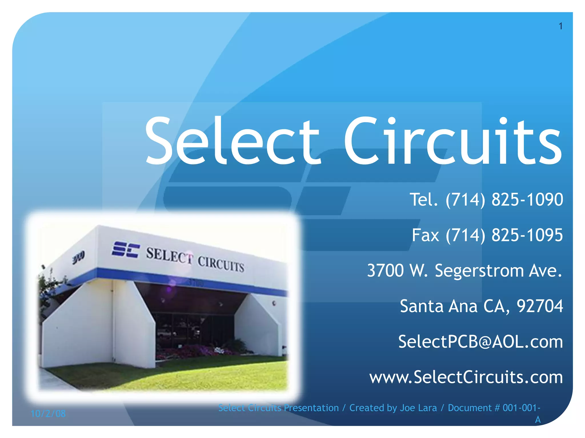
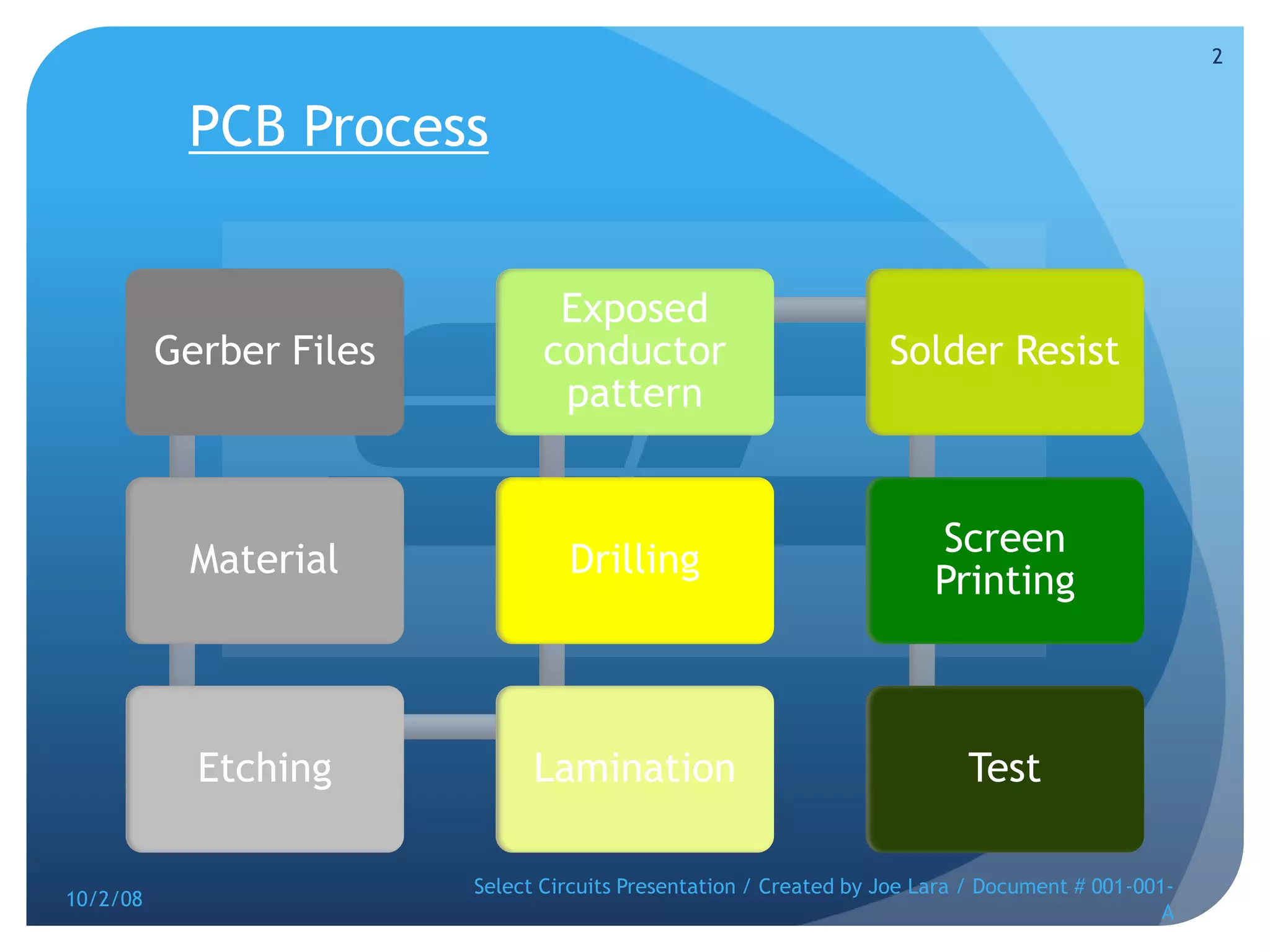
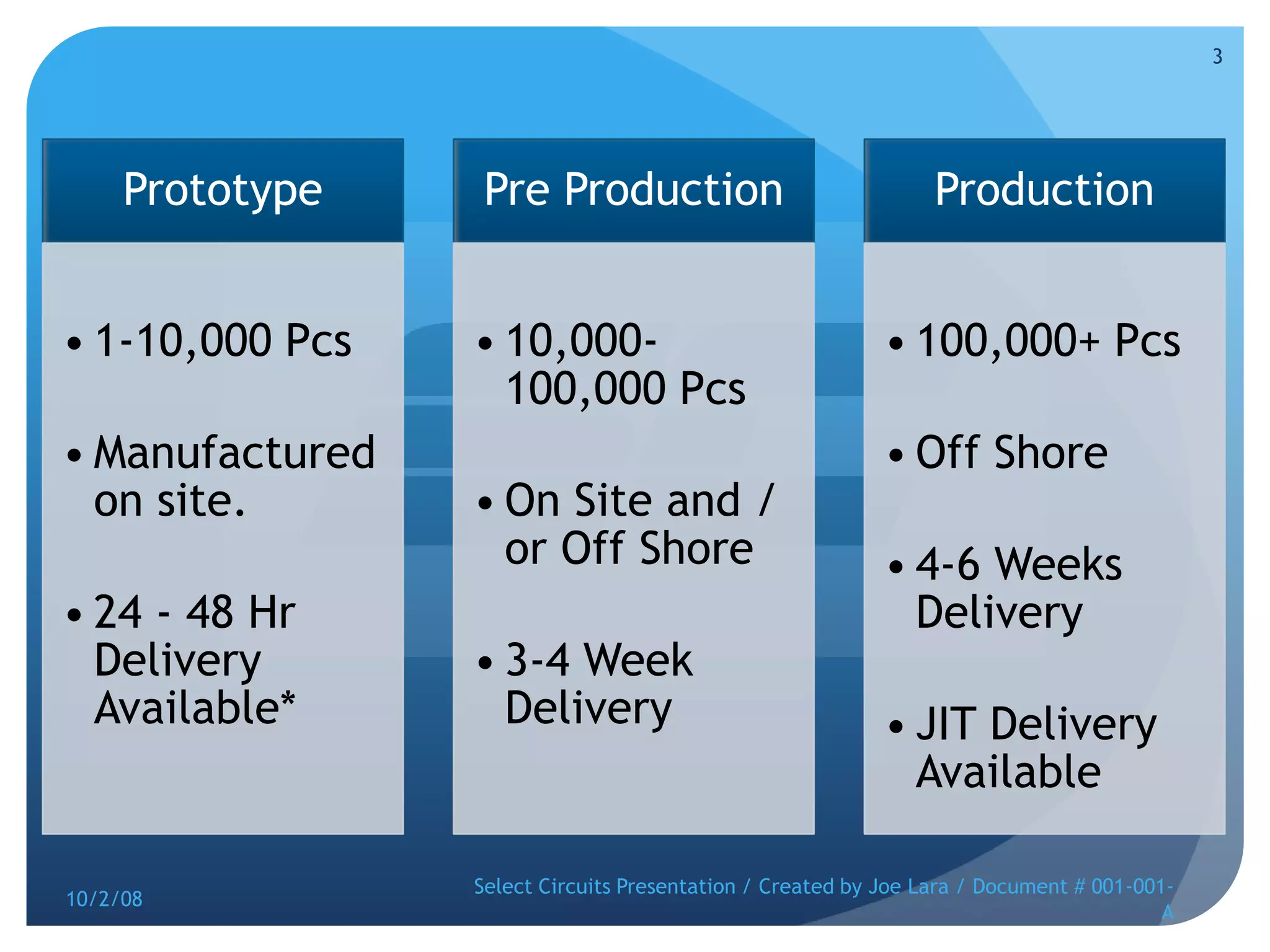
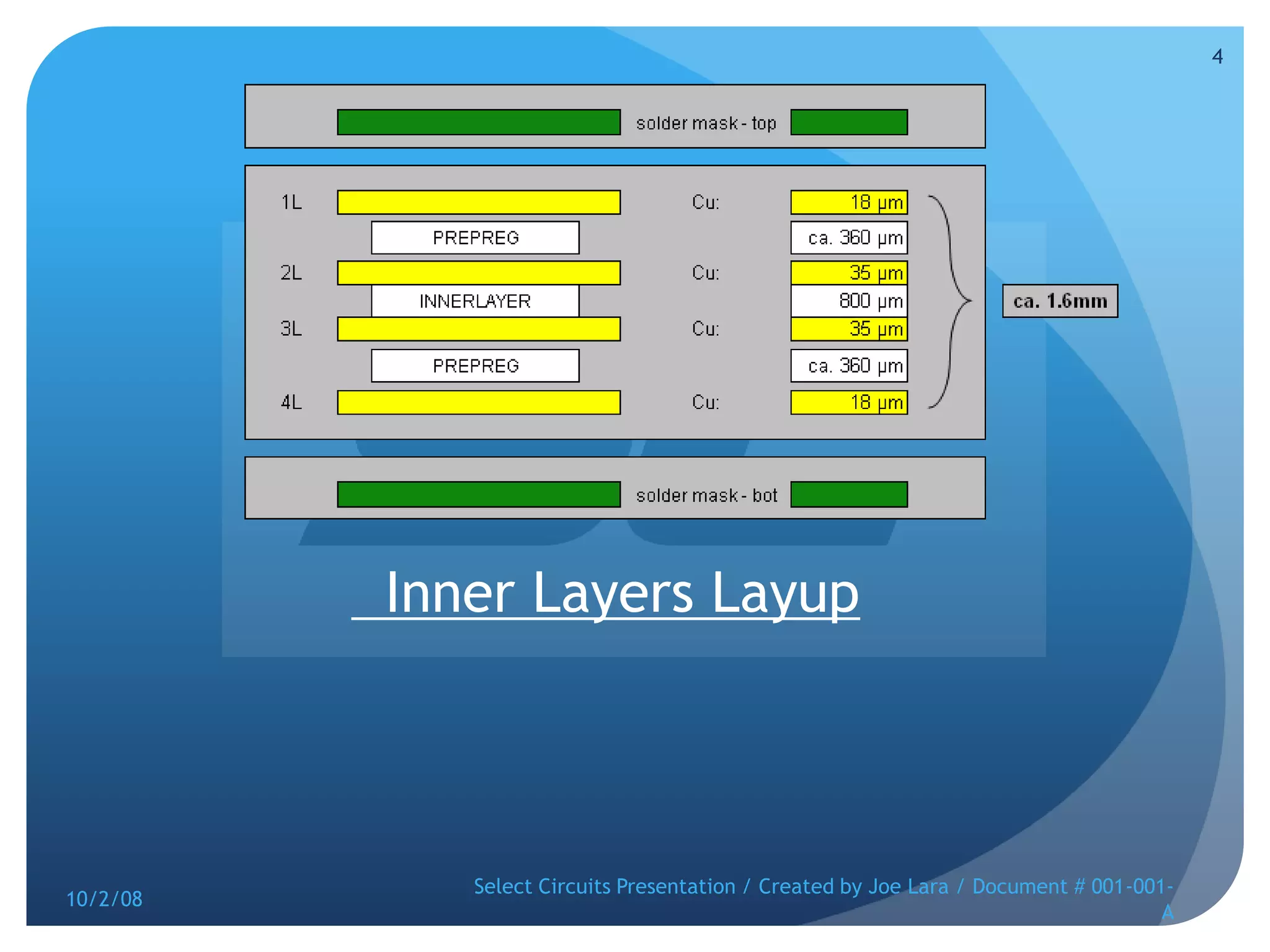
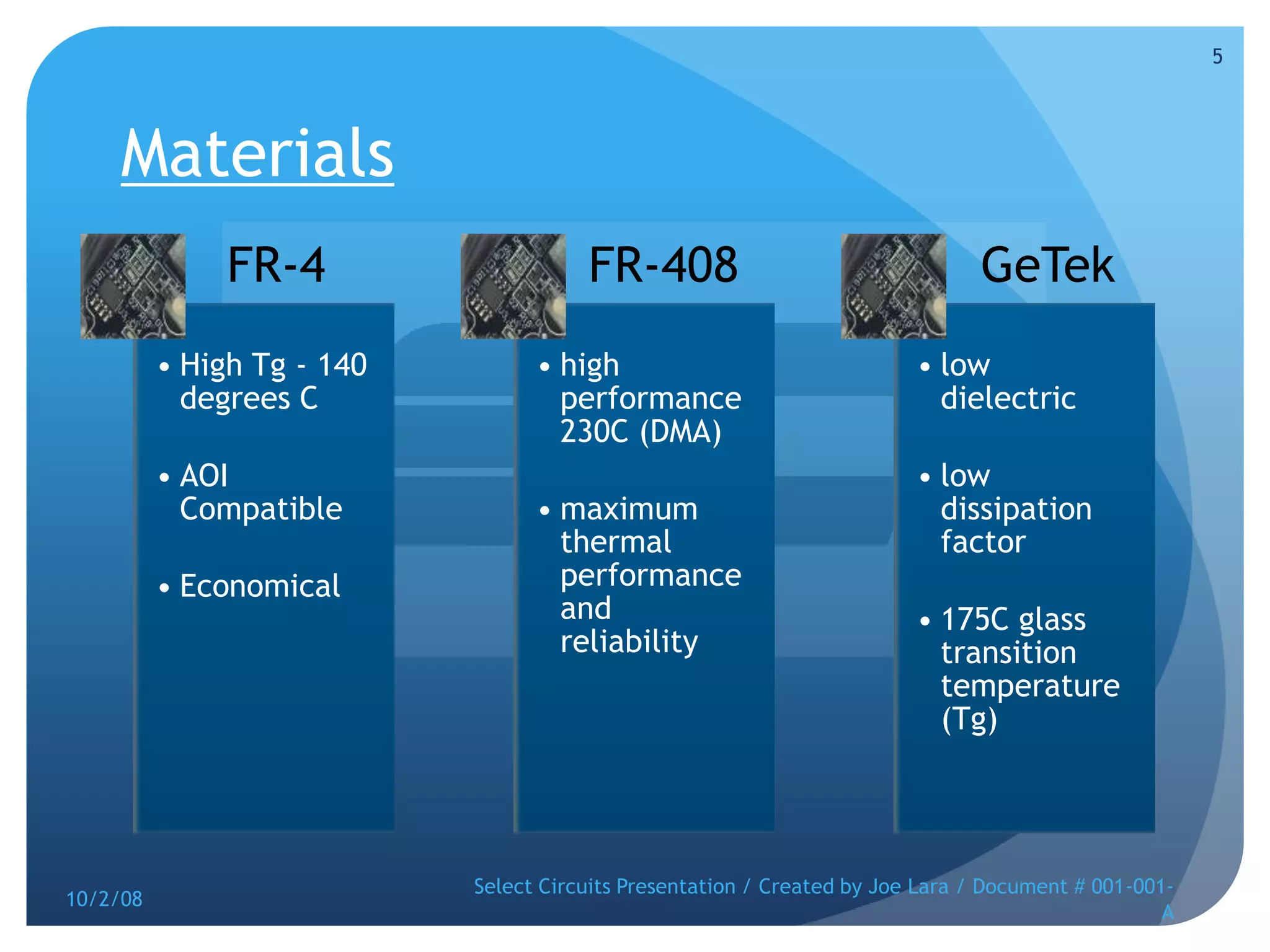
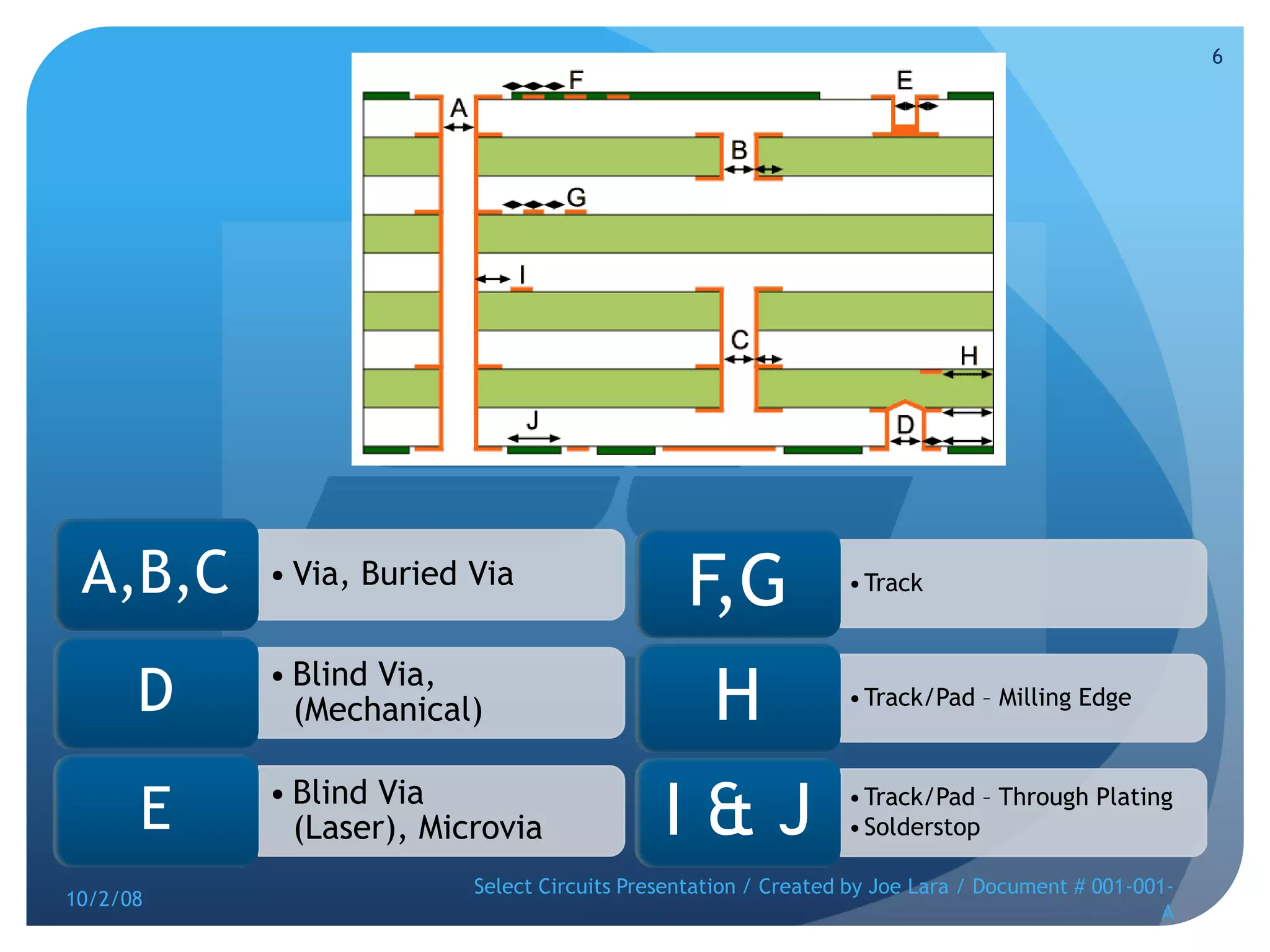
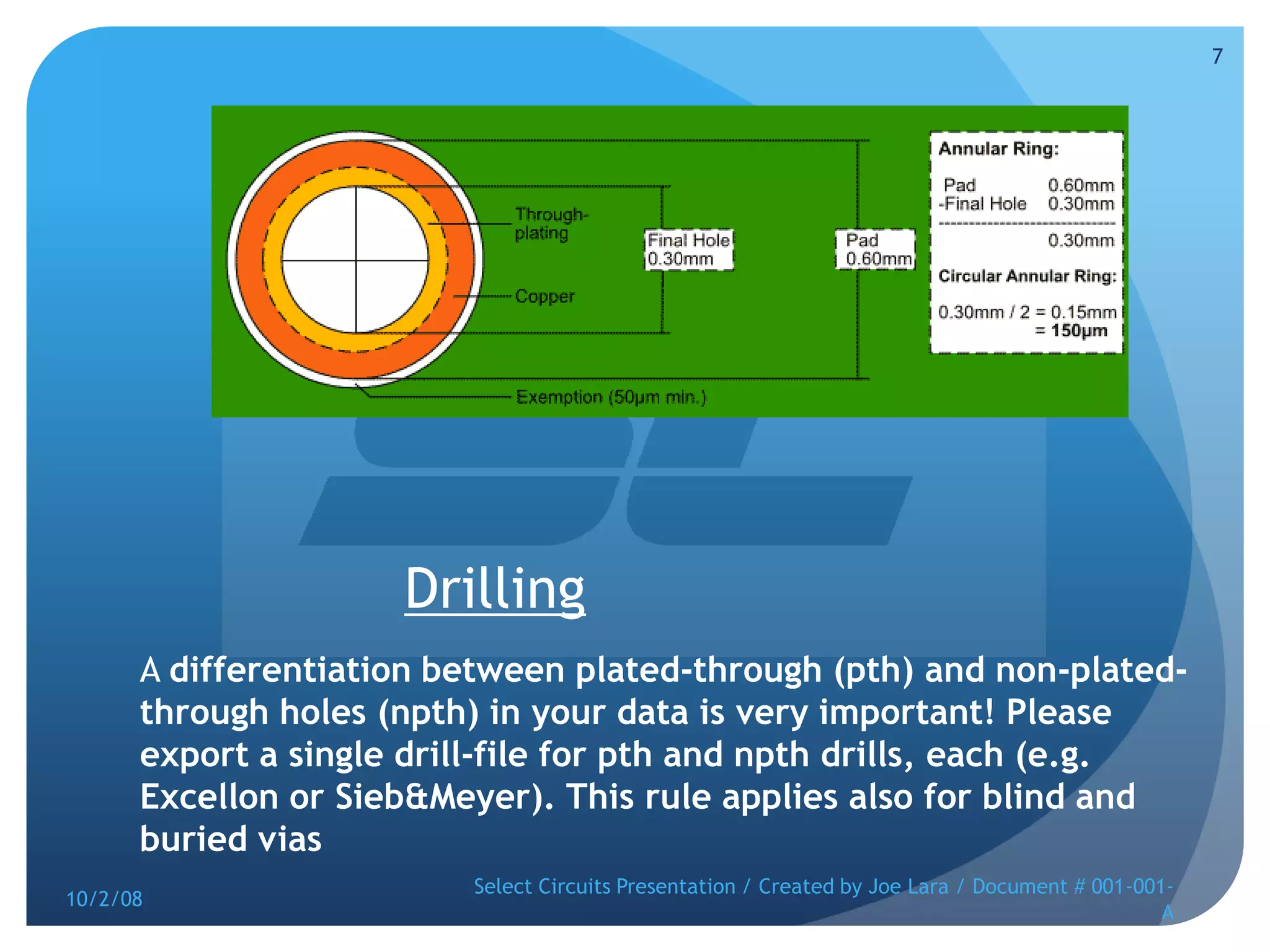
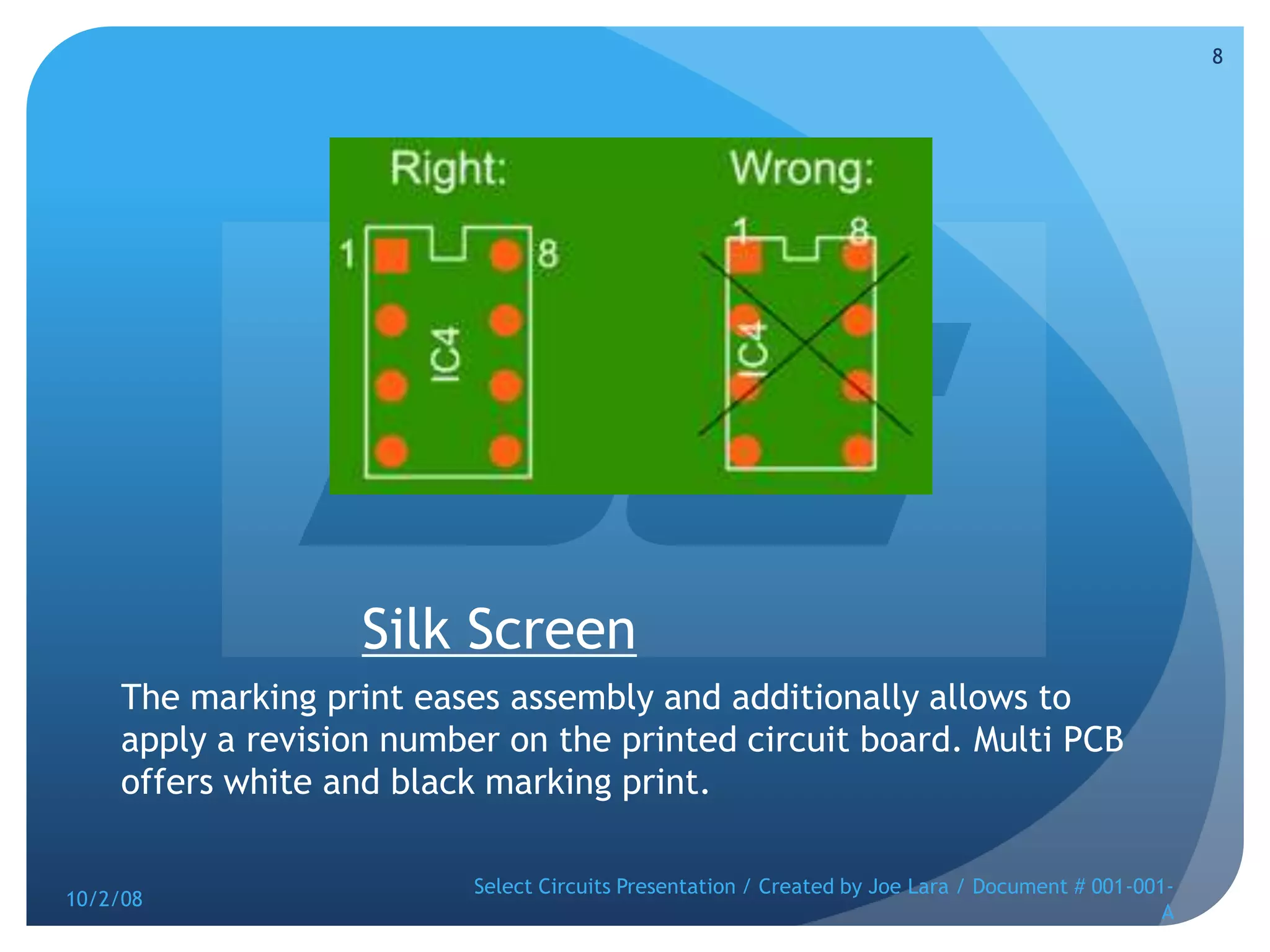
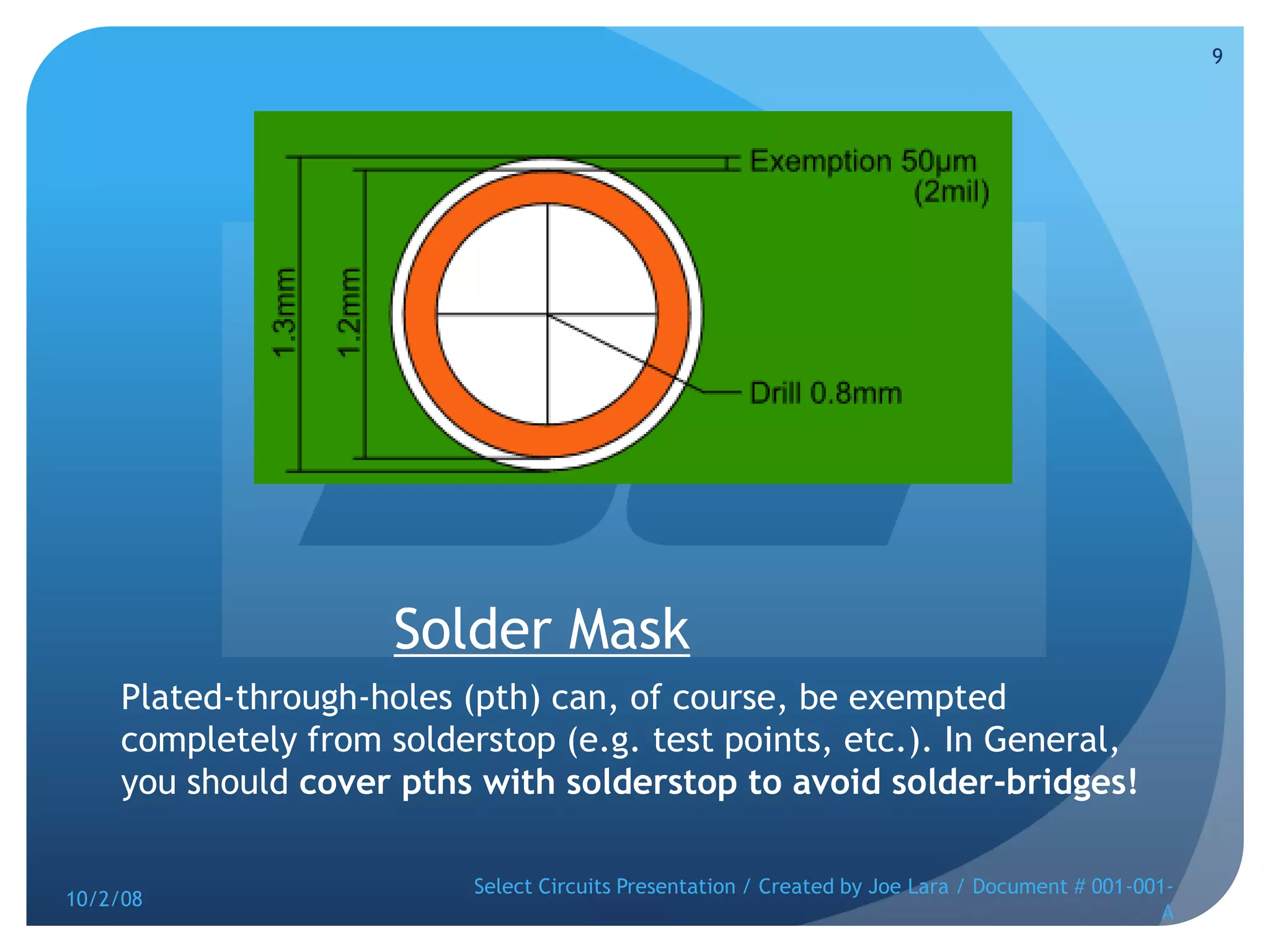
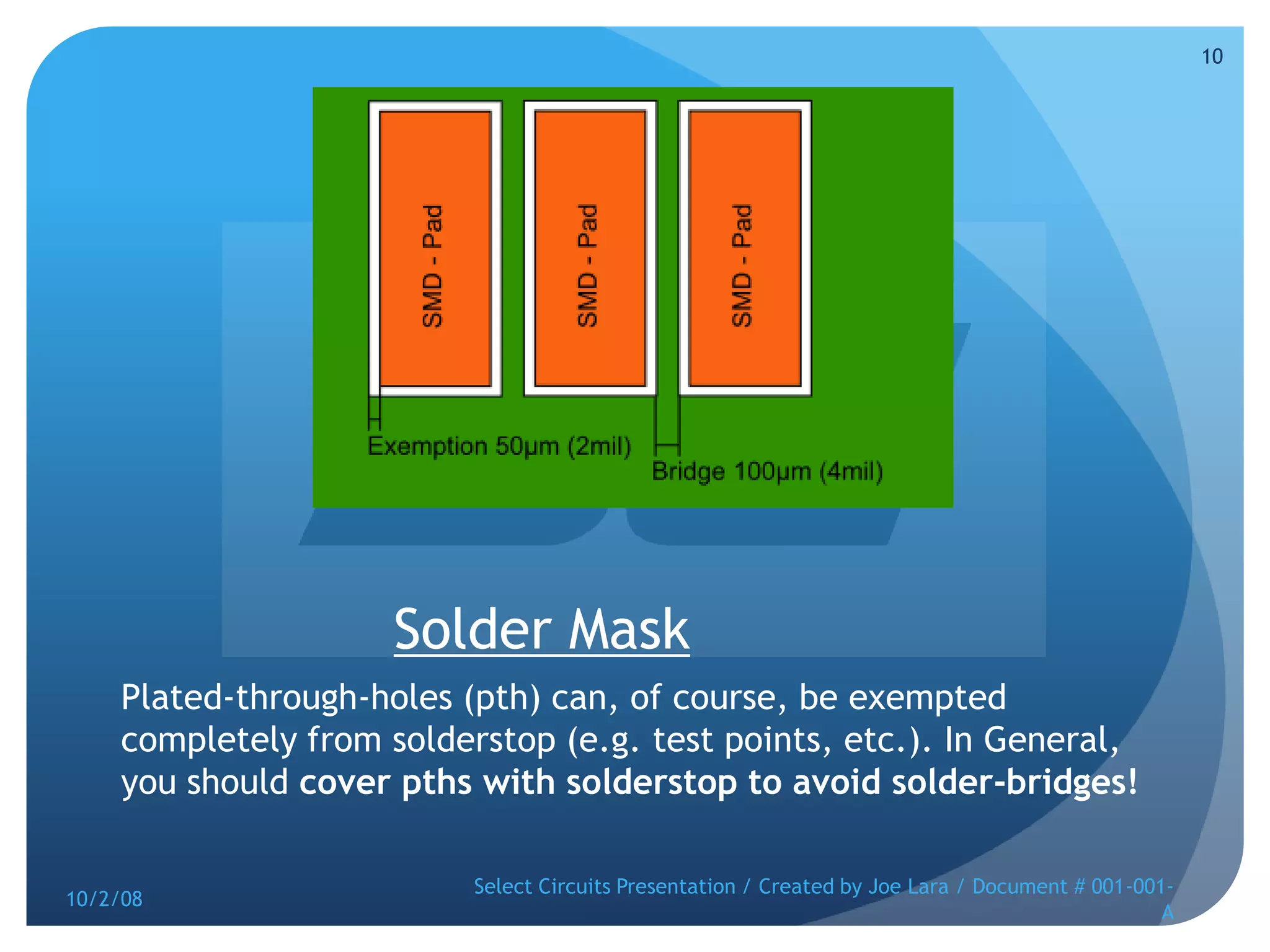
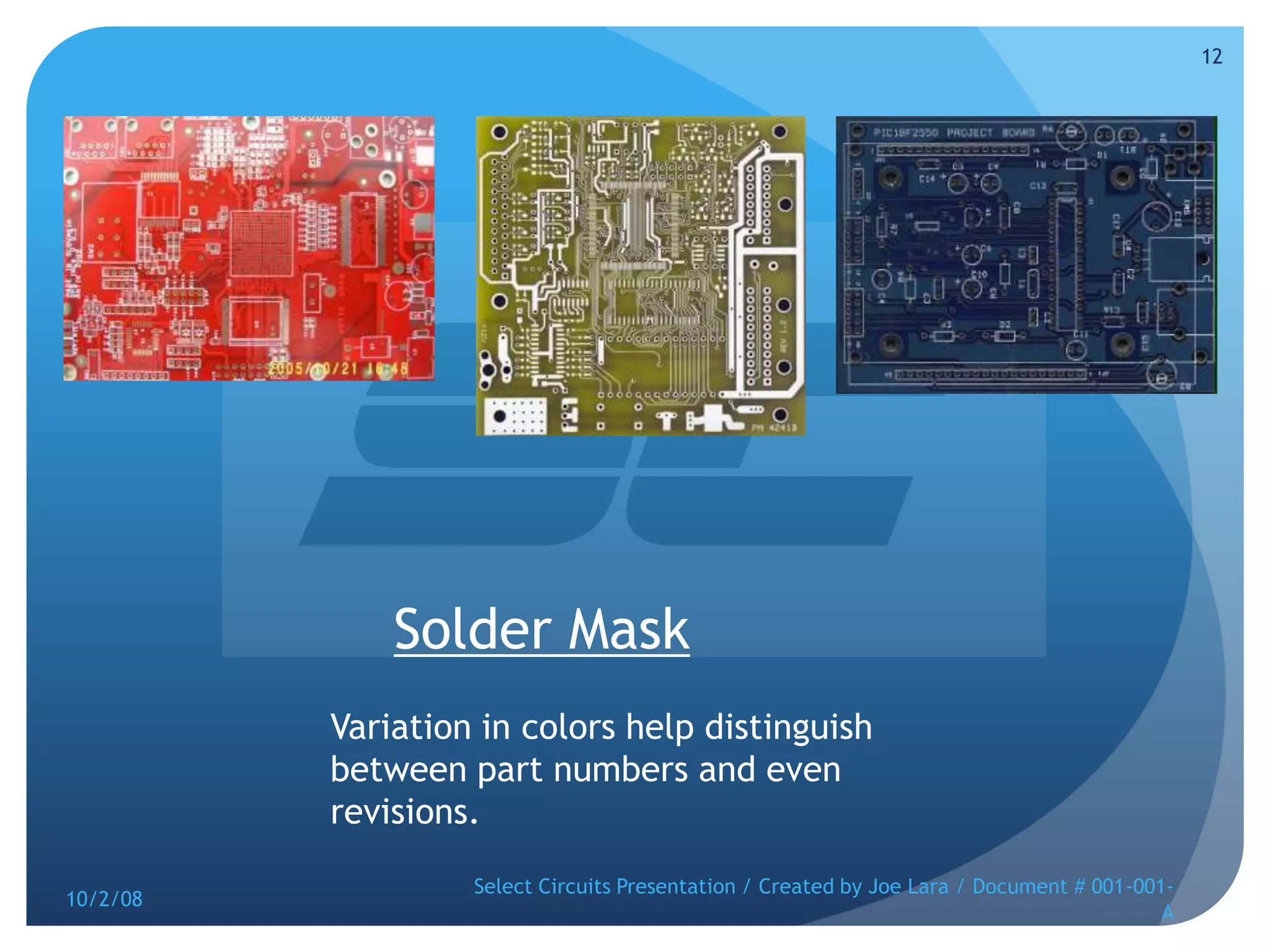
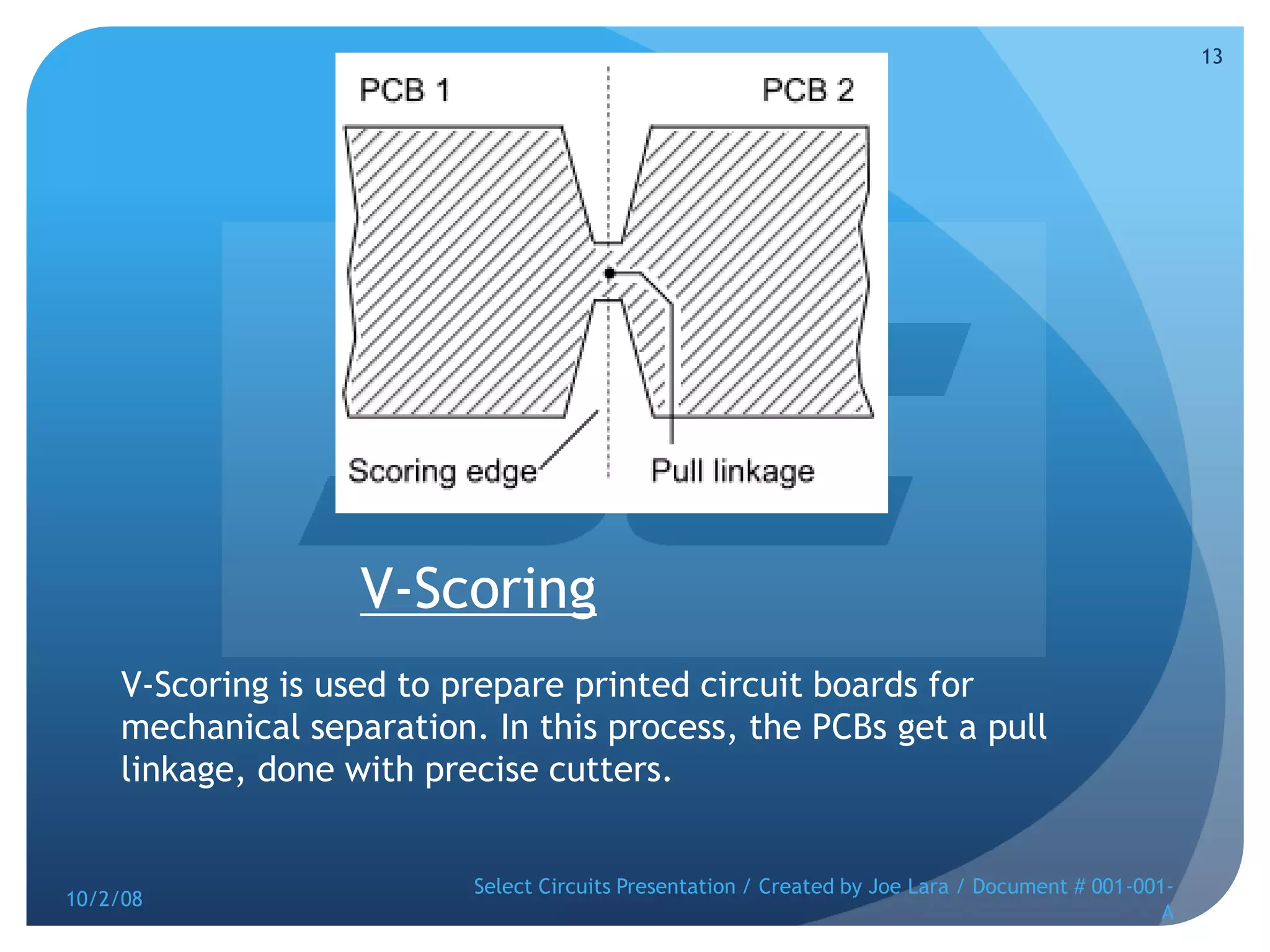
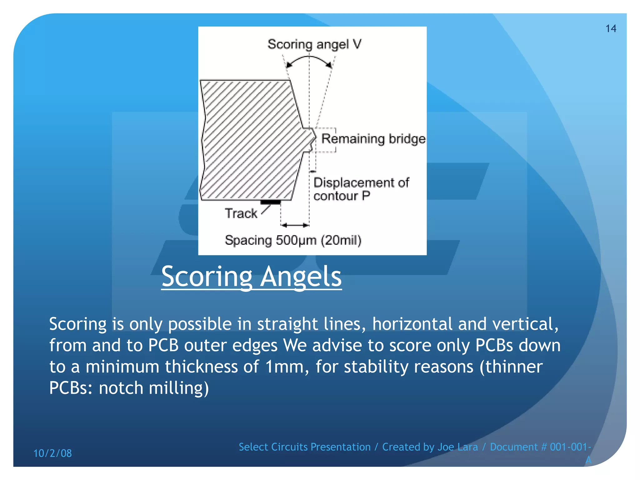
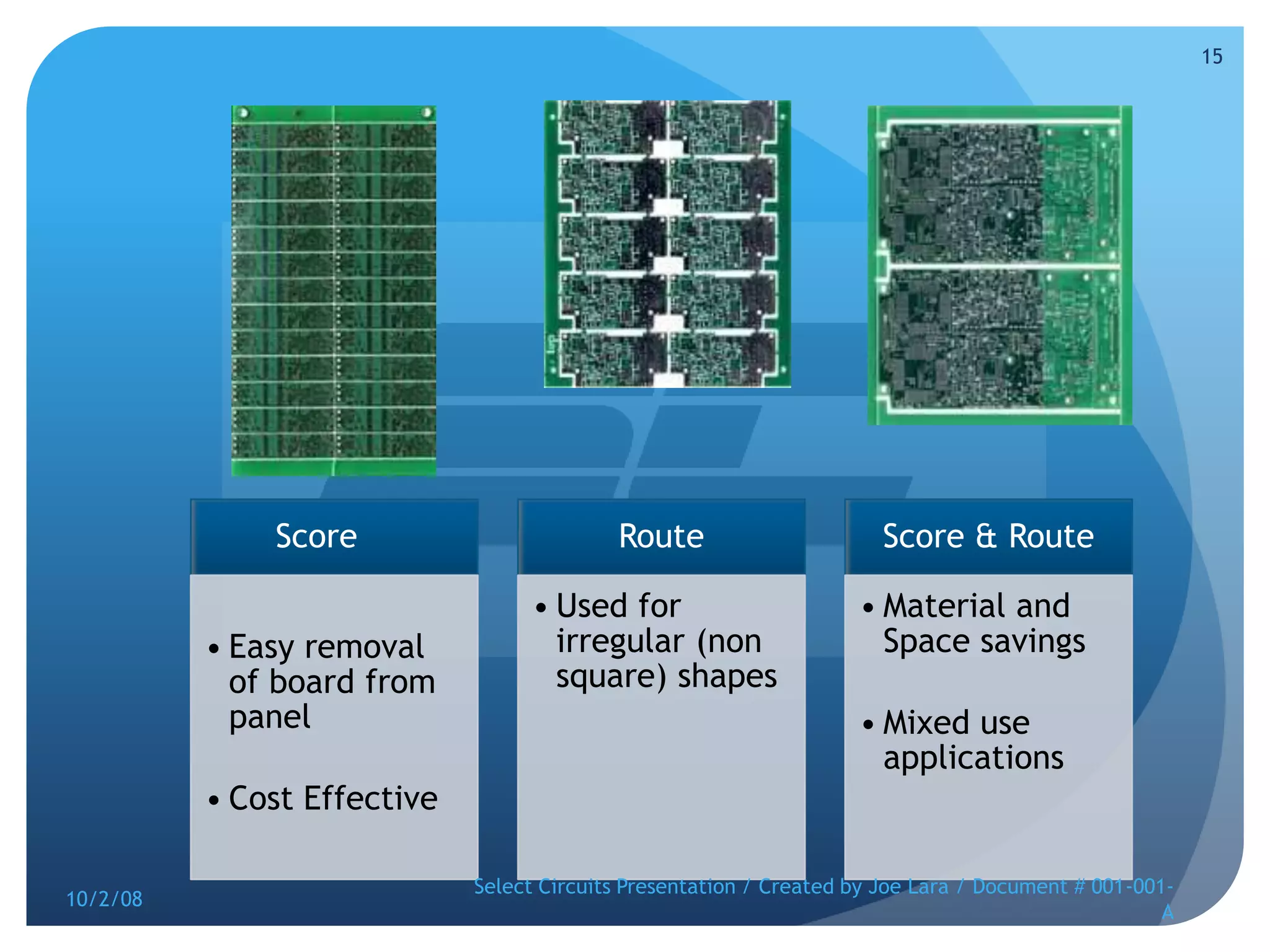
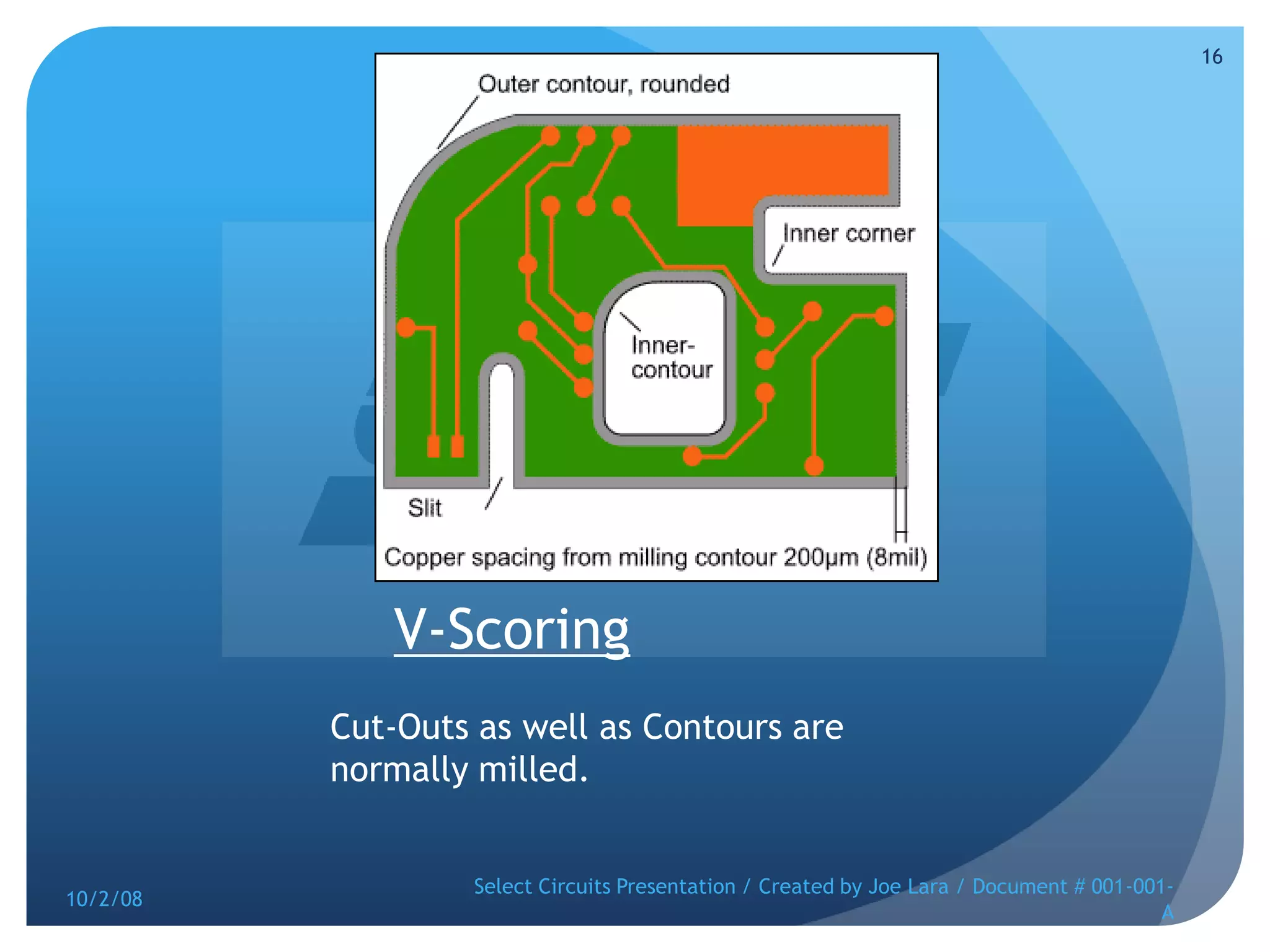
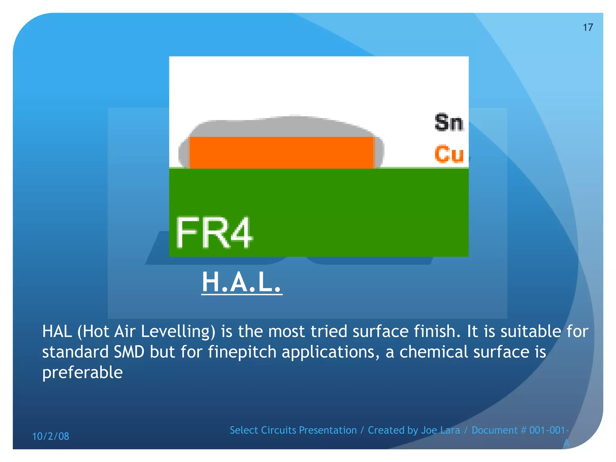
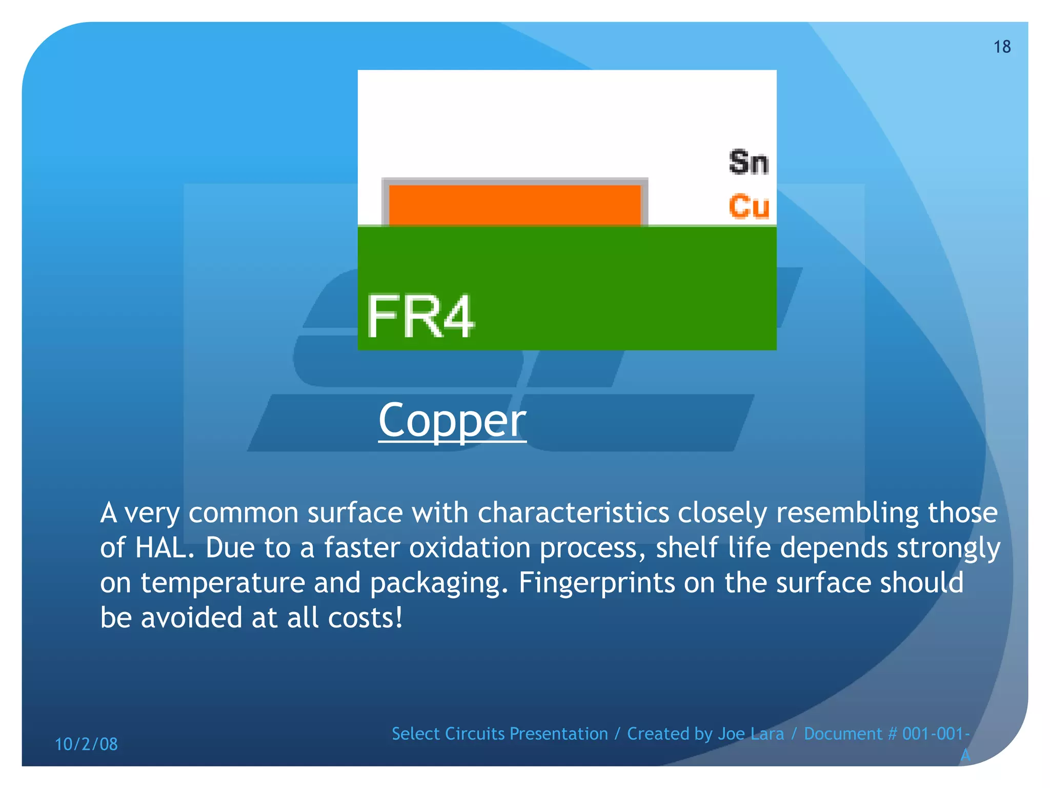
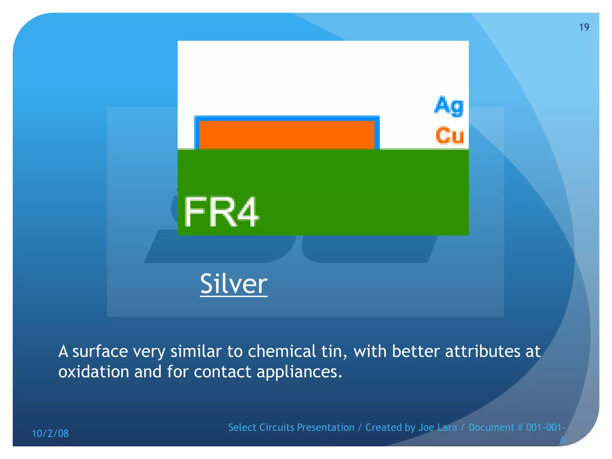
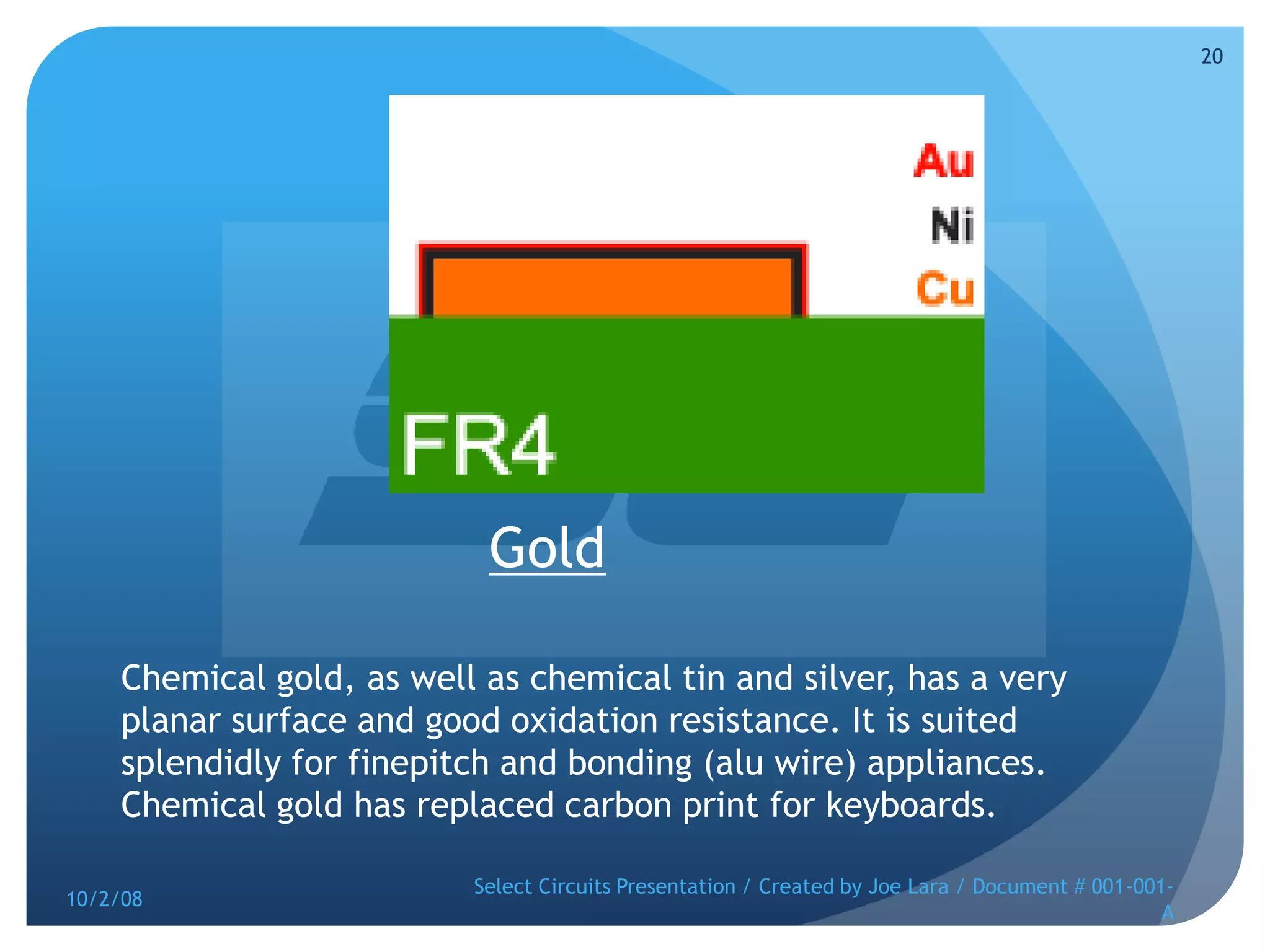
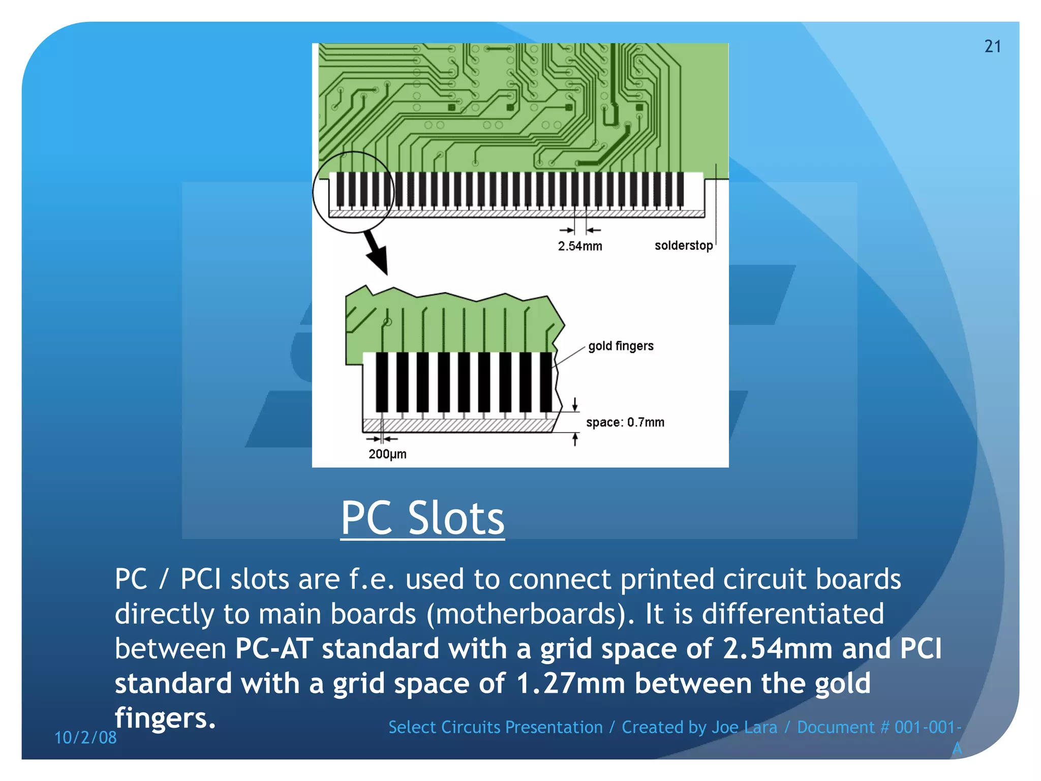
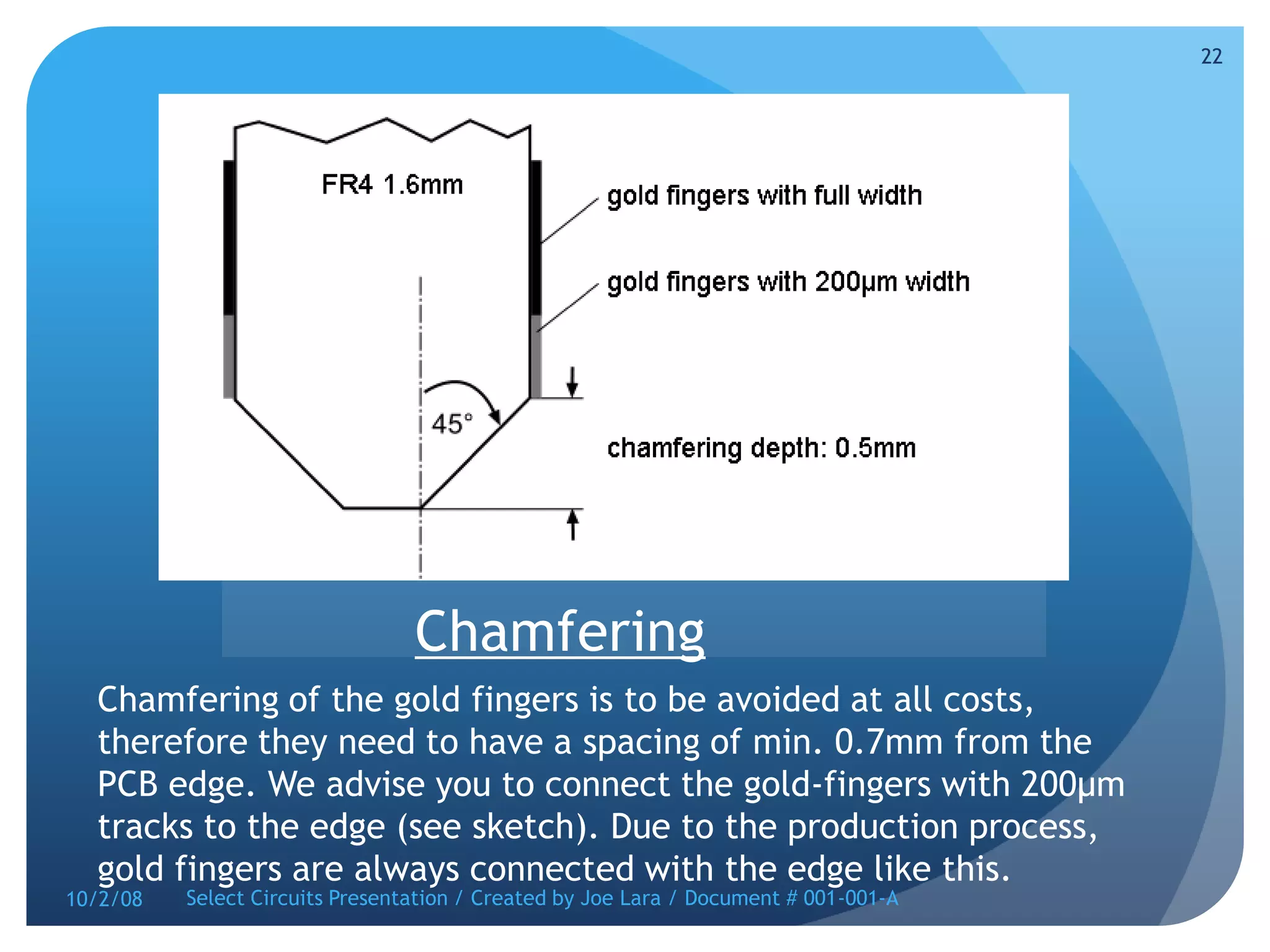
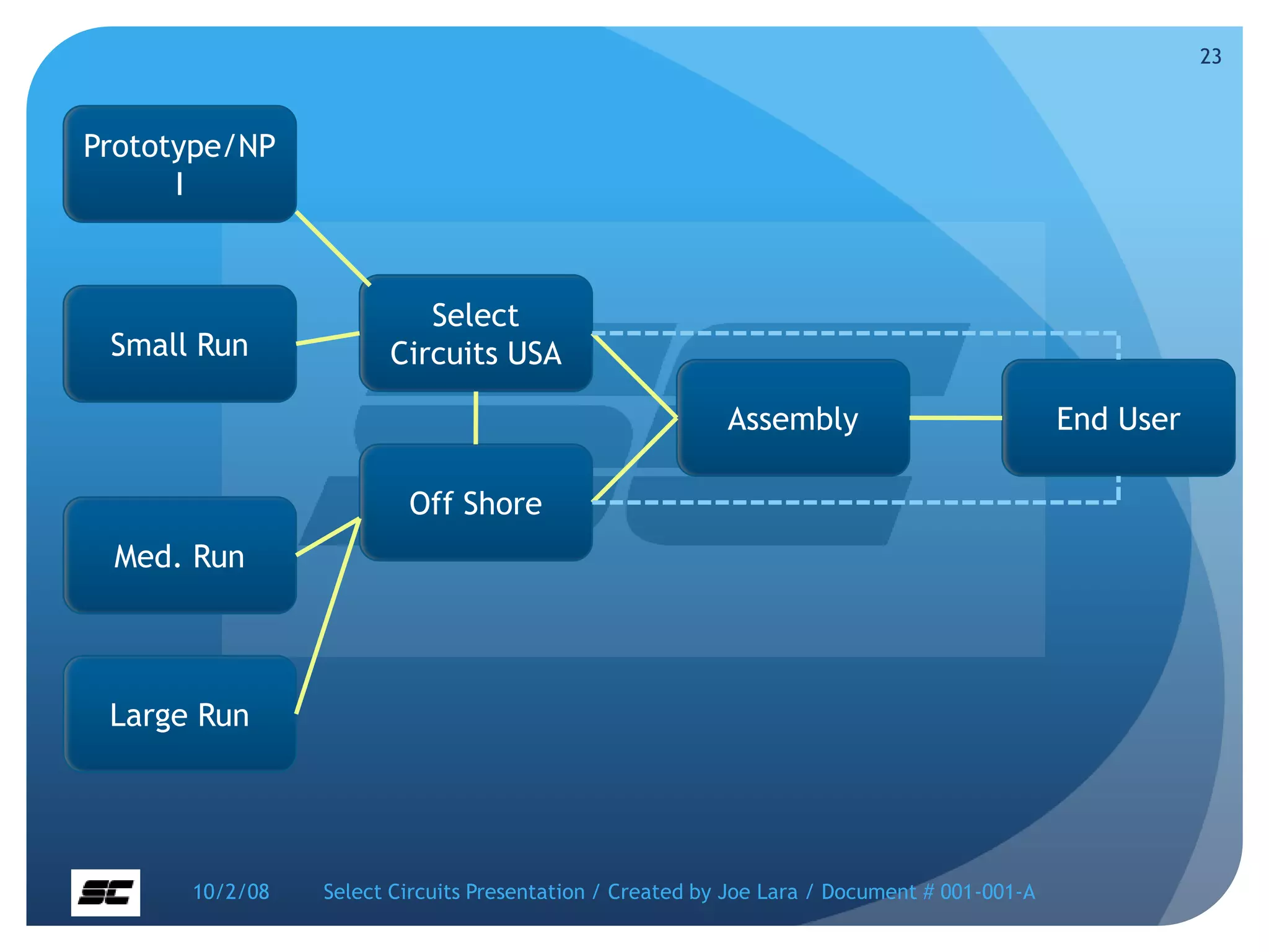
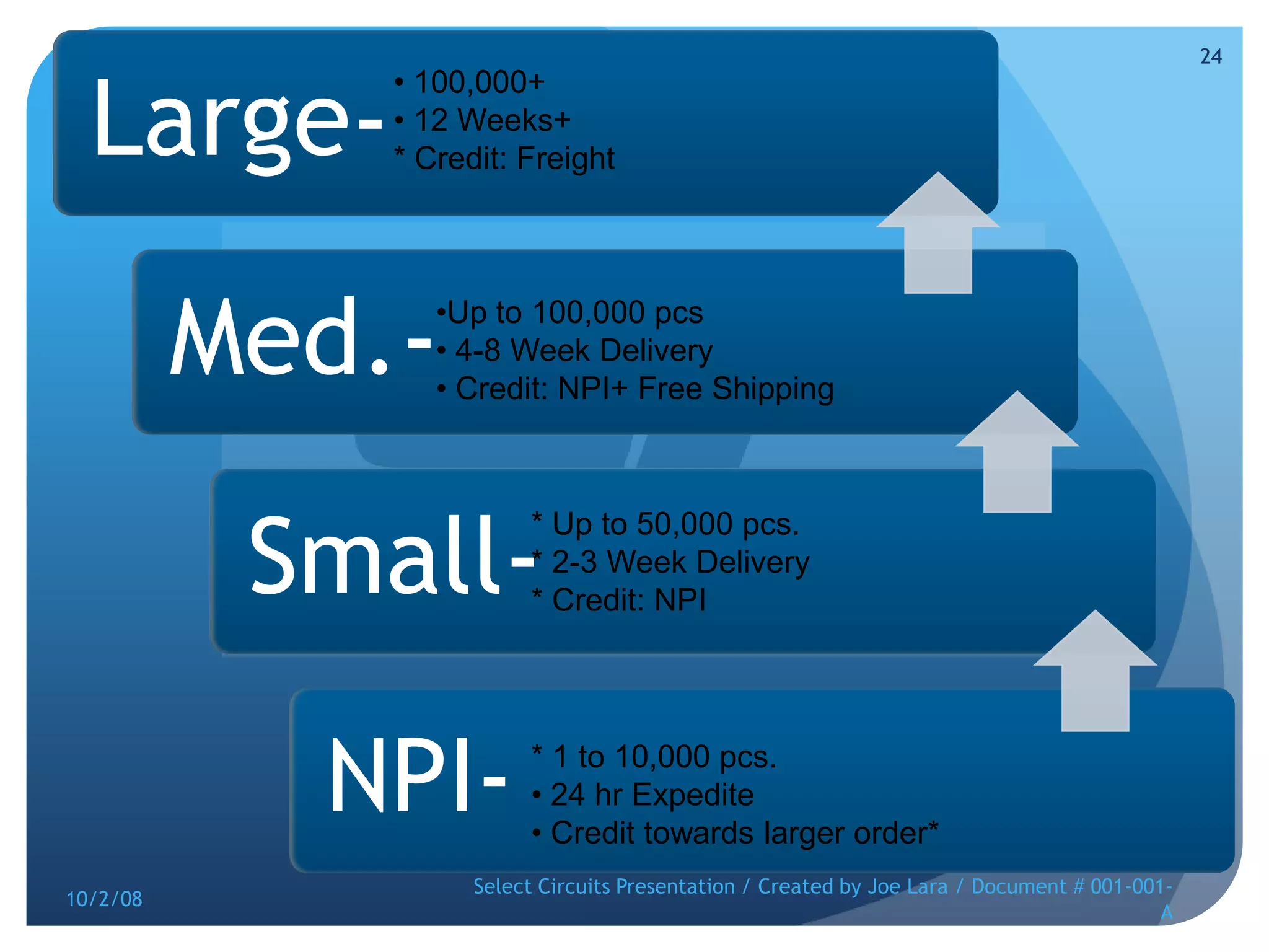
The document is a presentation from Select Circuits that discusses their printed circuit board (PCB) manufacturing process. It covers the various stages of PCB production including inner layer layup, materials used, drilling, silk screening, solder masking, heat sinks, surface finishes, and gold plating of connectors. It also provides information on Select Circuits' prototype, small run, and large volume production capabilities.
PCB Production Introduction /How to Make PCB will separated with 3 parts to introduce about printed circuit boards PCB basic, different PCB types, PCB material, PCB sheet, PCB production process, main PCB manufacturing process include PCB drilling, plated through hole, dry film,PCB etching, solder mask, different PCB surface finishing and so on...
High Voltage PCB Design Presentation by AltiumAltium
Looking for High Voltage PCB design resources?
Take a look at Altium's resources for electrical engineers and PCB designers here.
Or view the original presentation at: https://resources.altium.com/presentations/high-voltage-pcb-design-presentation
Or for even more information on High Voltage PCB Design, click here:
https://resources.altium.com/pcb-design-blog/high-voltage-pcb-design-creepage-and-clearance-distance
Introduce production process of Aluminum base Printed Circuit boards with high thermal conductivity, and solutions for some problems in production.Metal Core PCB, LED PCB, TCA, Dry film,PCB lamination, Gold plating Circuit boards, Stencil printing,PCB soldermask
Guide to datamate latches and jackscrews PTMHarwin plc
To help with your Datamate Connector identification and selection, here is a guide to the types of fixings available in the range, covering Latches, Jackscrews and the 101Lok fixing options.
IC adapter technologies document shows various configurations of probing and logic analyzer adapters for all SMT package types, as well as socket probes for DIP and PLCC. Partnered with Agilent and Tektronix, enabling adapters to facilitate the use of in-circuit emulators and FPGA development systems.
Not many customers know that we offer full PCB design and layout services here at Epec. Design and layout may not be a full-time employable position, so there are advantages of having your PCB fabricator complete the PCB design for you, not to mention the time needed to accomplish this task. So, rely on Epec to be an extension of your electrical engineering team.
PCB designs can be difficult to manufacture. Working in tandem with your circuit board supplier is beneficial to both you and your supplier. It can save cost, reduce manufacturing challenges and prototyping.
Knowing what is needed for quoting purpose and at the time of your order is key to a smooth process.
In this webinar, we review what is needed in terms of the Bill of Materials and schematic details to accurately quote and deliver the exact PCB design and layout that you require.
For more information on our custom PCB solutions, visit https://www.epectec.com/pcb/
Jetronics India, established as manufacturers of connectors in 1985, has grown into a leading producer and
exporter of MILC5015 grade electrical connectors and related accessories.
Communiqué de presse: le groupe Lamesch intègre un véhicule 100% électrique à...ALD Luxembourg
ALD Automotive a livrée à la société Lamesch sa première voiture 100% électrique le 22 mars 2013. Ce véhicule, Un Renault Kangoo Express ZE servira le personnel dans ses déplacements logistiques.
Análisis situacional de la ciberseguridad en perú y países sudamericanosMARIO HUAYPUNA
Este es un pequeño articulo que reune informacion de los ultimos años incluyendo este, acerca de la situacion de la ciberserguridad en Peru y en Sudamerica haciendo incapie en como se maneja esta problematica en los gobiernos y entidades publicas y privadas.
Abb Combiflex Lugs 1.5, Abb Combiflex Lugs 2.5 | AKBAR TRADING EST. JUBAILAKBAR TRADING
Contact sockets, silver plated (set of 100 pcs)
10 A, conductor area 0,25-1,5 mm2
20 A, conductor area 1,5-2,5 mm2
1
1
1MRK 002 136-A
1MRK 002 136-D
50 g
90 g
Contact pins, silver plated (set of 100 pcs)
10 A, conductor area 0,25-1,5 mm2
20 A, conductor area 1,5-2,5 mm2
1
1
1MRK 002 136-G
1MRK 002 136-H
60 g
120 g
Harwin’s Gecko (G125 series) connectors provide a low profile, dual row interconnect solution for cable-to-board, cable-to-cable and board-to-board. The product is ideally suited for stacking and cable mating in areas where PCB real estate is at a premium.
1. Select Circuits Tel. (714) 825-1090 Fax (714) 825-1095 3700 W. Segerstrom Ave. Santa Ana CA, 92704 SelectPCB@AOL.com www.SelectCircuits.com 10/2/08 Select Circuits Presentation / Created by Joe Lara / Document # 001-001-A 1
2. PCB Process 10/2/08 Select Circuits Presentation / Created by Joe Lara / Document # 001-001-A 2
7. Drilling A differentiation between plated-through (pth) and non-plated-through holes (npth) in your data is very important! Please export a single drill-file for pth and npth drills, each (e.g. Excellon or Sieb&Meyer). This rule applies also for blind and buried vias 10/2/08 Select Circuits Presentation / Created by Joe Lara / Document # 001-001-A 7
8. Silk Screen The marking print eases assembly and additionally allows to apply a revision number on the printed circuit board. Multi PCB offers white and black marking print. 10/2/08 Select Circuits Presentation / Created by Joe Lara / Document # 001-001-A 8
9. Solder Mask Plated-through-holes (pth) can, of course, be exempted completely from solderstop (e.g. test points, etc.). In General, you should cover pths with solderstop to avoid solder-bridges! 10/2/08 Select Circuits Presentation / Created by Joe Lara / Document # 001-001-A 9
10. Solder Mask Plated-through-holes (pth) can, of course, be exempted completely from solderstop (e.g. test points, etc.). In General, you should cover pths with solderstop to avoid solder-bridges! 10/2/08 Select Circuits Presentation / Created by Joe Lara / Document # 001-001-A 10
11. Heat Sink Heat Sink help transfer heat to an area where it can be better dissipated. 10/2/08 Select Circuits Presentation / Created by Joe Lara / Document # 001-001-A 11
12. Solder Mask Variation in colors help distinguish between part numbers and even revisions. 10/2/08 Select Circuits Presentation / Created by Joe Lara / Document # 001-001-A 12
13. V-Scoring V-Scoring is used to prepare printed circuit boards for mechanical separation. In this process, the PCBs get a pull linkage, done with precise cutters. 10/2/08 Select Circuits Presentation / Created by Joe Lara / Document # 001-001-A 13
14. Scoring Angels Scoring is only possible in straight lines, horizontal and vertical, from and to PCB outer edges We advise to score only PCBs down to a minimum thickness of 1mm, for stability reasons (thinner PCBs: notch milling) 10/2/08 Select Circuits Presentation / Created by Joe Lara / Document # 001-001-A 14
16. V-Scoring Cut-Outs as well as Contours are normally milled. 10/2/08 Select Circuits Presentation / Created by Joe Lara / Document # 001-001-A 16
17. H.A.L. HAL (Hot Air Levelling) is the most tried surface finish. It is suitable for standard SMD but for finepitch applications, a chemical surface is preferable 10/2/08 Select Circuits Presentation / Created by Joe Lara / Document # 001-001-A 17
18. Copper A very common surface with characteristics closely resembling those of HAL. Due to a faster oxidation process, shelf life depends strongly on temperature and packaging. Fingerprints on the surface should be avoided at all costs! 10/2/08 Select Circuits Presentation / Created by Joe Lara / Document # 001-001-A 18
19. Silver A surface very similar to chemical tin, with better attributes at oxidation and for contact appliances. 10/2/08 Select Circuits Presentation / Created by Joe Lara / Document # 001-001-A 19
20. Gold Chemical gold, as well as chemical tin and silver, has a very planar surface and good oxidation resistance. It is suited splendidly for finepitch and bonding (alu wire) appliances. Chemical gold has replaced carbon print for keyboards. 10/2/08 Select Circuits Presentation / Created by Joe Lara / Document # 001-001-A 20
21. PC Slots PC / PCI slots are f.e. used to connect printed circuit boards directly to main boards (motherboards). It is differentiated between PC-AT standard with a grid space of 2.54mm and PCI standard with a grid space of 1.27mm between the gold fingers. 10/2/08 Select Circuits Presentation / Created by Joe Lara / Document # 001-001-A 21
22. Chamfering Chamfering of the gold fingers is to be avoided at all costs, therefore they need to have a spacing of min. 0.7mm from the PCB edge. We advise you to connect the gold-fingers with 200µm tracks to the edge (see sketch). Due to the production process, gold fingers are always connected with the edge like this. 10/2/08 Select Circuits Presentation / Created by Joe Lara / Document # 001-001-A 22
23. 23 Prototype/NPI Select Circuits USA Small Run Assembly End User Off Shore Med. Run Large Run 10/2/08 Select Circuits Presentation / Created by Joe Lara / Document # 001-001-A