Datasheet of CMF10120D(SiC MOSFET)
•
0 likes•1,191 views

Datasheet of CMF10120D(SiC MOSFET) in English

Recommended
More Related Content
What's hot
What's hot (20)
Viewers also liked
Viewers also liked (12)
Similar to Datasheet of CMF10120D(SiC MOSFET)
Similar to Datasheet of CMF10120D(SiC MOSFET) (20)
More from Tsuyoshi Horigome
More from Tsuyoshi Horigome (20)
Recently uploaded
Recently uploaded (20)
Datasheet of CMF10120D(SiC MOSFET)
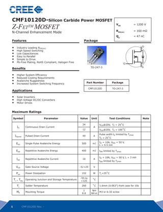
- 1. CMF10120D-Silicon Carbide Power MOSFET Z-FeTTM MOSFET VDS = 1200 V N-Channel Enhancement Mode mΩ RDS(on) = 160 Qg = 47 nC Features Package • Industry Leading RDS(on) D D • High Speed Switching • Low Capacitances • Easy to Parallel • Simple to Drive • Pb-Free Plating, RoHS Compliant, Halogen Free G G TO-247-3 S S Benefits • Higher System Efficiency • Reduced Cooling Requirements • Avalanche Ruggedness • Increased System Switching Frequency Part Number Package CMF10120D TO-247-3 Applications • Solar Inverters • High Voltage DC/DC Converters • Motor Drives Maximum Ratings Symbol Parameter Value Unit Test Conditions Note 24 VGS@20V, TC = 25˚C ID Continuous Drain Current A 12 VGS@20V, TC = 100˚C Pulse width tP limited by Tjmax IDpulse Pulsed Drain Current 49 A TC = 25˚C ID = 10A, VDD = 50 V, EAS Single Pulse Avalanche Energy 500 mJ L = 9.5 mH EAR Repetitive Avalanche Energy 400 mJ tAR limited by Tjmax ID = 10A, VDD = 50 V, L = 3 mH IAR Repetitive Avalanche Current 10 A tAR limited by Tjmax VGS Gate Source Voltage -5/+25 V Ptot Power Dissipation 152 W TC=25˚C -55 to TJ , Tstg Operating Junction and Storage Temperature +125 ˚C TL Solder Temperature 260 ˚C 1.6mm (0.063”) from case for 10s 1 Nm Md Mounting Torque 8.8 lbf-in M3 or 6-32 screw 1 CMF10120D Rev. -
- 2. Electrical Characteristics Symbol Parameter Min. Typ. Max. Unit Test Conditions Note V(BR)DSS Drain-Source Breakdown Voltage 1200 V VGS = -5V, ID = 50μA 2.5 4 VDS = VGS, ID = 500uA, TJ = 25ºC VGS(th) Gate Threshold Voltage V 1 1.8 VDS = VGS, ID = 500uA, TJ = 125ºC 0.5 50 VDS = 1200V, VGS = 0V, TJ = 25ºC IDSS Zero Gate Voltage Drain Current μA 5 125 VDS = 1200V, VGS = 0V, TJ = 125ºC IGSS Gate-Source Leakage Current 250 nA VGS = 20V, VDS = 0V 160 220 VGS = 20V, ID = 10A, TJ = 25ºC fig. 4 RDS(on) Drain-Source On-State Resistance mΩ 190 260 VGS = 20V, ID = 10A, TJ = 125ºC 3.7 VDS= 20V, IDS= 10A, TJ = 25ºC gfs Transconductance S fig. 3 3.4 VDS= 20V, IDS= 10A, TJ = 125ºC Ciss Input Capacitance 928 VGS = 0V Coss Output Capacitance 63 VDS = 800V pF fig. 5 f = 1MHz Crss Reverse Transfer Capacitance 7.45 VAC = 25mV td(on)i Turn-On Delay Time 7 tr Rise Time 14 VDD = 800V ns VGS = -2/20V td(off)i Turn-Off Delay Time 46 ID = 10A tfi Fall Time 37 fig. 12 RG = 6.8Ω EON 261 μJ L = 856μH Turn-On Switching Loss Per JEDEC24 Page 27 EOff 120 μJ Turn-Off Switching Loss RG Internal Gate Resistance 13.6 Ω VGS = 0V, f = 1MHz, VAC = 25mV NOTES: 1. The recommended on-state VGS is +20V and the recommended off-state VGS is between -2V and -5V Reverse Diode Characteristics Symbol Parameter Typ. Max. Unit Test Conditions Note 3.5 VGS = -5V, IF=5A, TJ = 25ºC Vsd Diode Forward Voltage V 3.1 VGS = -2V, IF=5A, TJ = 25ºC trr Reverse Recovery Time 138 ns VGS = -5V, IF=10A, TJ = 25ºC Qrr Reverse Recovery Charge 94 nC VR = 800V, fig. 13,14 diF/dt= 100A/μs Irrm Peak Reverse Recovery Current 1.57 A Thermal Characteristics Symbol Parameter Typ. Max. Unit Test Conditions Note RθJC Thermal Resistance from Junction to Case 0.66 RθCS Case to Sink, w/ Thermal Compound 0.25 °C/W fig. 6 RθJA Thermal Resistance From Junction to Ambient 40 Gate Charge Characteristics Symbol Parameter Typ. Max. Unit Test Conditions Note Qgs Gate to Source Charge 11.8 VDD = 800V fig.9 Qgd Gate to Drain Charge 21.5 nC ID =10A VGS = -2/20V Per JEDEC24-2 Qg Gate Charge Total 47.1 2 CMF10120D Rev. -
- 3. Typical Performance 60 50 0V =2 45 V GS 18V 20V V GS= 50 V GS= 40 16V 18V V GS= V GS= 35 40 V GS= 14V 6V 30 V GS=1 ID (A) 25 ID (A) 30 VGS=12V VGS=14V 20 20 15 VGS=10V VGS=12V 10 10 VGS=10V 5 0 0 0 5 10 15 20 0 5 10 15 20 VDS (V) VDS (V) Fig 1. Typical Output Characteristics TJ = 25ºC Fig 2. Typical Output Characteristics TJ = 125ºC 30 25 VDS =25V 20 T = 125°C 15 ID(A) VGS=20V 10 T = 25°C 5 0 0 5 10 15 20 VGS(V) Figure 3. Typical Transfer Characteristics Fig 4. Normalized On-Resistance vs. Temperature 10000 10000 10000 10000 VGS = 0 V VGS = 0 V VGS = 0 V VGS = 0 V f = 1 MHz f = 1 MHz fC 1 MHz = f = 1 MHz Ciss Ciss Ciss iss 1000 1000 1000 1000 Capacitance (pF) Capacitance (pF) Capacitance (pF) Capacitance (pF) Coss Coss Coss Coss 100 100 100 100 Crss Crss Crss Crss 10 10 10 10 1 1 1 1 0 200 0 400 200 600 400 800 600 800 0 0 50 50100 150 100 200 150 200 VDS (V) VDS (V) VDS (V) VDS (V) Fig 5A and 5B. Typical Capacitance vs. Drain – Source Voltage 3 CMF10120D Rev. -
- 4. Typical Performance 1 Thermal Resistance (°C/W) 0.1 0.01 0.001 0.0001 1E-6 10E-6 100E-6 1E-3 10E-3 100E-3 1 10 Time (sec) Fig 6. Transient Thermal Impedence, Junction - Case 400 350 Switching Energy(μJ) 300 Switching Energy(μJ) 250 200 VGS= -2/20V 150 VGS= -2/20V RG= 11.8Ω Total RG= 11.8Ω Total VDD= 800V 100 VDD= 800V ID= 10A ID= 10A 50 0 0 2 4 6 8 10 12 14 Drain Current(A) Drain Current(A) Fig 7. Inductive Switching Energy(Turn-on) vs. ID Fig 8. Inductive Switching Energy(Turn-off) vs ID 20 300 250 15 Switching Energy (µJ) 200 10 EON VGS (V) EOFF ID=10A 150 VDD=800V 5 100 0 50 -5 0 0 10 20 30 40 50 25 45 65 85 105 125 Gate Charge (nC) Temp ( C) Fig 9. Typical Gate Charge Characteristics @ 25°C Fig 10. Inductive Switching Energy vs. Temp 4 CMF10120D Rev. -
- 5. Clamped Inductive Switch Testing Fixture tw pulse duration VGS(on) 90% 90% Input (Vi) 50% 50% 10% 10% VGS(off) C2D10120D 856μH 10A, 1200V Input Pulse Input Pulse SiC Schottky Rise Time Fall Time + 800V - 42.3μf td(on)i tfi td(off)i tri iD(on) CMF10120D 10% D.U.T. 10% Output (iD) 90% 90% iD(off) ton(i) toff(i) Fig 11. Switching Waveform Test Circuit Fig 12. Switching Test Waveform Times trr Ic trr ∫ Qrr= id dt tx tx 10% Irr Vcc 856μH CMF10120D 10% Vcc D.U.T. Vpk + Irr 800V - 42.3μf Diode Recovery Waveforms CMF10120D t2 Diode Reverse Recovery Energy ∫ Erec= id dt t1 t1 t2 Fig 13. Body Diode Recovery Waveform Fig 14. Body Diode Recovery Test 5 CMF10120D Rev. -
- 6. EA = 1/2L x ID2 Fig 15. Avalanche Test Circuit Fig 16. Theoretical Avalanche Waveform Package Dimensions Package TO-247-3 Inches Millimeters POS Min Max Min Max A .190 .205 4.83 5.21 A1 .090 .100 2.29 2.54 A2 .075 .085 1.91 2.16 b .042 .052 1.07 1.33 b1 .075 .095 1.91 2.41 b2 .075 .085 1.91 2.16 b3 .113 .133 2.87 3.38 b4 .113 .123 2.87 3.13 c .022 .027 0.55 0.68 D .819 .831 20.80 21.10 D1 .640 .695 16.25 17.65 D2 .037 .049 0.95 1.25 E .620 .635 15.75 16.13 E1 .516 .557 13.10 14.15 E2 .145 .201 3.68 5.10 E3 .039 .075 1.00 1.90 E4 .487 .529 12.38 13.43 e .214 BSC 5.44 BSC D D D N 3 3 L .780 .800 19.81 20.32 L1 .161 .173 4.10 4.40 ØP .138 .144 3.51 3.65 Q .216 .236 5.49 6.00 G G G S .238 .248 6.04 6.30 S SS 6 CMF10120D Rev. -
- 7. Recommended Solder Pad Layout TO-247-3 Part Number Package CMF10120D TO-247-3 “The levels of environmentally sensitive, persistent biologically toxic (PBT), persistent organic pollutants (POP), or otherwise restricted materials in this product are below the maximum concentration values (also referred to as the threshold limits) permitted for such substances, or are used in an exempted application, in accordance with EU Directive 2002/95/EC on the restriction of the use of certain hazardous substances in electrical and electronic equipment (RoHS), as amended through April 21, 2006. This product has not been designed or tested for use in, and is not intended for use in, applications implanted into the human body nor in applications in which failure of the product could lead to death, personal injury or property damage, including but not limited Cree, Inc. to equipment used in the operation of nuclear facilities, life-support machines, cardiac defibrillators or similar emergency medical 4600 Silicon Drive equipment, aircraft navigation or communication or control systems, air traffic control systems, or weapons systems. Durham, NC 27703 USA Tel: +1.919.313.5300 Copyright © 2010-2011 Cree, Inc. All rights reserved. The information in this document is subject to change without notice. Cree Fax: +1.919.313.5451 and the Cree logo are registered trademarks and Z-REC and Z-FET are trademarks of Cree, Inc. www.cree.com/power 7 CMF10120D Rev. -
- 8. Applications Information: The Cree SiC DMOSFET has removed the upper voltage limit of silicon MOSFETs. However, there are some differences in characteristics when compared to what is usually expected with high voltage silicon MOSFETs. These differences need to be carefully addressed to get maximum benefit from the SiC DMOSFET. In general, although the SiC DMOSFET is a superior switch compared to its silicon counter- parts, it should not be considered as a direct drop-in replacement in existing appli- cations. There are two key characteristics that need to be kept in mind when applying the SiC DMOSFETs; modest transconductance and no turn-off tail. The modest trans- conductance requires that VGS needs to be 20V to optimize performance. This can be seen the Output and Transfer Characteristics shown in Figures 1-3. The modest transconductance also affects the transition where the device behaves as a voltage controlled resistance to where it behaves as a voltage controlled current source as a function of VDS. The result is that the transition occurs over higher values of VDS than is usually experienced with Si MOSFETs and IGBTs. This might affect the operation anti-desaturation circuits, especially if the circuit takes advantage of the device entering the constant current region at low values of forward voltage. The modest transconductance needs to be carefully considered in the design of the gate drive circuit. The first obvious requirement is that the gate driver be capable of a 22V (or higher) swing. The recommended on state VGS is +20V and the rec- ommended off state VGS is between -2V to -5V. Please carefully note that although the gate voltage swing is higher than typical silicon MOSFETs and IGBTs, the to- tal gate charge of the SiC DMOSFET is considerably lower. In fact, the product of gate voltage swing and gate charge for the SiC DMOSFET is lower than comparable silicon devices. The gate voltage must have a fast dV/dt to achieve fast switching times which indicates that a very low impedance driver is necessary. 2.5VLastly, the fidelity of the gate drive pulse must be carefully controlled. The nominal threshold voltage is 2.3V and the device is not fully on (dVDS/dt ≈ 0) until the VGS is above 16V. This is a noticeably wider range than what is typically experienced with sili- con MOSFETs and IGBTs. The net result of this is that the SiC DMOSFET has a somewhat lower ‘noise margin’. Any excessive ringing that is present on the gate drive signal could cause unintentional turn-on or partial turn-off of the device. The gate resistance should be carefully selected to insure that the gate drive pulse is adequately dampened. To first order, the gate circuit can be approximated as a 8 CMF10120D Rev. -
- 9. RLOOP CGATE 1 RLOOP LLOOP 2 LLOOP VPULSE CGATE LLOOP RLOOP 2 CGATE As shown, minimizing LLOOP minimizes the value of RLOOP needed for critical As shown, minimizing L L dampening. MinimizingLOOP minimizes the value of RLOOP needed for critical is also minimizes the rise/fall time. Therefore, it strongly recommended that the gate drive bethe rise/fall close to the SiC DMOSFET dampening. Minimizing LLOOP also minimizes located as time. Therefore, it is LOOP as possible to minimize that . Angate driveresistance of 6.8 Ω wasthe SiC DMOSFET strongly recommended L LOOP the external be located as close to used to characterizeto minimize LLOOP. An external resistance of resistance can be used so as possible this device. Lower values of external gate 6.8 Ω was used to long as the gate device. Lower maintained. In the event that no can be used characterize this pulse fidelity is values of external gate resistance external gateso resistance is used, it is fidelity is maintained. In current be that no external gate long as the gate pulse suggested that the gate the event checked to indirectly verify that is used, nois suggested thatin the gate circuit.be checked toaccomplished resistance there is it ringing present the gate current This can be indirectly with a that there is no ringing present in the gate circuit.setup is a two-stage verify very small current transformer. A recommended This can be accomplished currentvery small current transformer. A recommended setup is a two-stage with a transformer as shown below: current transformer as shown below: IG SENSE VCC GATE DRIVER GATE DRIVE INPUT T1 SiC DMOSFET + - VEE The two stage current transformer first stage consists of 10 turns of AWG 30 wire on a two stage current transformer first stage consists of 10 turns recommended. The small high permeability core. A Ferroxcube 3E27 material is of AWG 30 wire Theasecondhigh permeabilitywide bandwidth current transformer, such as the on small stage is a small core. A Ferroxcube 3E27 material is recommended. Tektronix CT-2. Lastly, a separate source return should be used for theas thedrive The second stage is a small wide bandwidth current transformer, such gate as shown below: Lastly, a separate source return should be used for the gate drive Tektronix CT-2. as shown below: 9 CMF10120D Rev. -
- 10. Stray inductance on source lead causes load di/dt to be Kelvin gate connection with separate fed back into gate drive which causes the following: source return is highly recommended • Switch di/dt is limited • Could cause oscillation LOAD CURRENT 20V 20V R GATE SiC DMOS R GATE DRIVE SiC DMOS DRIVE L STRAY LOAD CURRENT A significant benefit of the SiC DMOSFET is the elimination of the tail current observed in silicon IGBTs. However, it is very important to note that the current tail does provide a certain degree of parasitic dampening during turn-off. Additional ringing and overshoot is typically observed when silicon IGBTs is replaced with SiC DMOSFETs. The additional voltage overshoot can be high enough to destroy the device. Therefore, it is critical to manage the output interconnection parasitics (and snubbers) to keep the ringing and overshoot from becoming problematic. ESD RATINGS ESD Test Total Devices Sampled Resulting Classification ESD-HBM All Devices Passed 1000V 2 (>2000V) ESD-MM All Devices Passed 400V C (>400V) ESD-CDM All Devices Passed 1000V IV (>1000V) 10 CMF10120D Rev. -