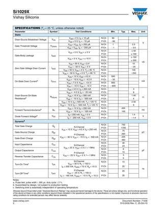
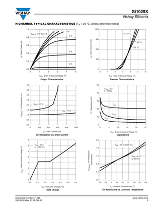
SlideShare a Scribd company logo
1 of 10
Download to read offline
Si1029X
                                                                                                                                  Vishay Siliconix

             Complementary N- and P-Channel 60 V (D-S) MOSFET

  PRODUCT SUMMARY                                                                   FEATURES
                    VDS (V)            RDS(on) ()           ID (mA)                • Halogen-free According to IEC 61249-2-21
                                                                                      Definition
                                  1.40 at VGS = 10 V              500
   N-Channel          60                                                            • TrenchFET® Power MOSFETs
                                   3 at VGS = 4.5 V               200               • Very Small Footprint
                                  4 at VGS = - 10 V           - 500                 • High-Side Switching
   P-Channel          - 60                                                          • Low On-Resistance:
                                  8 at VGS = - 4.5 V              - 25
                                                                                      N-Channel, 1.40 
                                                                                      P-Channel, 4 
                                                                                    • Low Threshold: ± 2 V (typ.)
                SC-89                                                               • Fast Switching Speed: 15 ns (typ.)
                                                                                    • Gate-Source ESD Protected: 2000 V
  S1
        1                     6   D1                                                • Compliant to RoHS Directive 2002/95/EC

                                                      Marking Code: H
  G1    2                     5   G2                                                BENEFITS
                                                                                    •    Ease in Driving Switches
  D2    3                     4   S2                                                •    Low Offset (Error) Voltage
                                                                                    •    Low-Voltage Operation
               Top View                                                             •    High-Speed Circuits
Ordering Information: Si1029X-T1-GE3 (Lead (Pb)-free and Halogen-free)
                                                                                    APPLICATIONS
                                                                                    • Replace Digital Transistor, Level-Shifter
                                                                                    • Battery Operated Systems
                                                                                    • Power Supply Converter Circuits


 ABSOLUTE MAXIMUM RATINGS (TA = 25 °C, unless otherwise noted)
                                                                                             N-Channel                          P-Channel
 Parameter                                                           Symbol             5s        Steady State            5s         Steady State   Unit
 Drain-Source Voltage                                                     VDS                   60                                - 60
                                                                                                                                                     V
 Gate-Source Voltage                                                      VGS                                  ± 20
                                                     TA = 25 °C                     320               305             - 200               - 190
 Continuous Drain Current (TJ = 150 °C)a                                   ID
                                                     TA = 85 °C                     230               220             - 145               - 135
                                                                                                                                                    mA
 Pulsed Drain Currentb                                                     IDM                 650                                - 650
 Continuous Source Current (Diode Conduction)a                             IS       450               380             - 450               - 380
                                                     TA = 25 °C                     280               250                 280             250
 Maximum Power Dissipationa                                                PD                                                                       mW
                                                     TA = 85 °C                     145               130                 145             130
 Operating Junction and Storage Temperature Range                        TJ, Tstg                           - 55 to 150                              °C
 Gate-Source ESD Rating (HBM, Method 3015)                                ESD                                 2000                                   V
Notes:
a. Surface mounted on FR4 board.
b. Pulse width limited by maximum junction temperature.


Document Number: 71435                                                                                                                      www.vishay.com
S10-2432-Rev. C, 25-Oct-10                                                                                                                               1
Si1029X
Vishay Siliconix

  SPECIFICATIONS (TJ = 25 °C, unless otherwise noted)
  Parameter                                 Symbol                          Test Conditions                            Min.         Typ.        Max.        Unit
  Static
                                                                   VGS = 0 V, ID = 10 µA                   N-Ch         60
  Drain-Source Breakdown Voltage               VDS
                                                                   VGS = 0 V, ID = - 10 µA                 P-Ch        - 60
                                                                                                                                                             V
                                                                  VDS = VGS, ID = 250 µA                   N-Ch          1                      2.5
  Gate Threshold Voltage                     VGS(th)
                                                                  VDS = VGS, ID = - 250 µA                 P-Ch         -1                     - 3.0
                                                                                                           N-Ch                                ± 50
                                                                   VDS = 0 V, VGS = ± 5 V
                                                                                                           P-Ch                                ± 100
  Gate-Body Leakage                           IGSS
                                                                                                           N-Ch                                ± 150
                                                                  VDS = 0 V, VGS = ± 10 V
                                                                                                           P-Ch                                ± 200
                                                                                                                                                             nA
                                                                   VDS = 50 V, VGS = 0 V                   N-Ch                                  10
                                                                  VDS = - 50 V, VGS = 0 V                  P-Ch                                 - 25
  Zero Gate Voltage Drain Current              IDSS
                                                           VDS = 50 V, VGS = 0 V, TJ = 85 °C               N-Ch                                 100
                                                           VDS = - 50 V, VGS = 0 V, TJ = 85 °C             P-Ch                                - 250
                                                                  VDS = 10 V, VGS = 4.5 V                  N-Ch         500
                                                               VDS = - 10 V, VGS = - 4.5 V                 P-Ch         - 50
  On-State Drain Currenta                     ID(on)                                                                                                        mA
                                                                VDS = 7.5 V, VGS = - 4.5 V                 N-Ch         800
                                                                VDS = - 10 V, VGS = - 10 V                 P-Ch        - 600
                                                                VGS = 4.5 V, ID = 200 mA                   N-Ch                                  3
                                                               VGS = - 4.5 V, ID = - 25 mA                 P-Ch                                  8
  Drain-Source On-State                                          VGS = 10 V, ID = 500 mA                   N-Ch                                 1.40
                                             RDS(on)                                                                                                         
  Resistancea                                                  VGS = - 10 V, ID = - 500 mA                 P-Ch                                  4
                                                          VGS = 10 V, ID = 500 mA, TJ = 125 °C             N-Ch                                 2.50
                                                         VGS = - 10 V, ID = - 500 mA, TJ = 125 °C          P-Ch                                  6
                                                                 VDS = 10 V, ID = 200 mA                   N-Ch                     200
  Forward Transconductancea                    gfs                                                                                                           ms
                                                               VDS = - 10 V, ID = - 100 mA                 P-Ch                     100
                                                                  IS = 200 mA, VGS = 0 V                   N-Ch                                  1.4
  Diode Forward Voltagea                       VSD                                                                                                           V
                                                                 IS = - 200 mA, VGS = 0 V                  P-Ch                                 - 1.4
  Dynamicb
                                                                                                           N-Ch                     750
  Total Gate Charge                            Qg                       N-Channel                          P-Ch                    1700
                                                           VDS = 10 V, VGS = 4.5 V, ID = 250 mA
                                                                                                           N-Ch                      75
  Gate-Source Charge                           Qgs                                                                                                           pC
                                                                        P-Channel                          P-Ch                     260
                                                         VDS = - 30 V, VGS = - 15 V, ID = - 500 mA         N-Ch                     225
  Gate-Drain Charge                            Qgd
                                                                                                           P-Ch                    460
                                                                                                           N-Ch                      30
  Input Capacitance                            Ciss                    N-Channel                           P-Ch                     23
                                                             VDS = 25 V, VGS = 0 V, f = 1 MHz
                                                                                                           N-Ch                      6
  Output Capacitance                          Coss                                                                                                           pF
                                                                        P-Channel                          P-Ch                     10
                                                            VDS = - 25 V, VGS = 0 V, f = 1 MHz             N-Ch                      3
  Reverse Transfer Capacitance                 Crss
                                                                                                           P-Ch                      5
                                                                        N-Channel                          N-Ch                      15
  Turn-On Timec                                tON                VDD = 30 V, RL = 150 
                                                           ID  200 mA, VGEN = 10 V, Rg = 10              P-Ch                      20
                                                                                                                                                             ns
                                                                        P-Channel                          N-Ch                      20
  Turn-Off   Timec                             tOFF              VDD = - 25 V, RL = 150 
                                                         ID  - 165 mA, VGEN = - 10 V, Rg = 10            P-Ch                      35

Notes:
a. Pulse test; pulse width  300 µs, duty cycle  2 %.
b. Guaranteed by design, not subject to production testing.
c. Switching time is essentially independent of operating temperature.
Stresses beyond those listed under “Absolute Maximum Ratings” may cause permanent damage to the device. These are stress ratings only, and functional operation
of the device at these or any other conditions beyond those indicated in the operational sections of the specifications is not implied. Exposure to absolute maximum
rating conditions for extended periods may affect device reliability.


www.vishay.com                                                                                                                      Document Number: 71435
2                                                                                                                                 S10-2432-Rev. C, 25-Oct-10
Si1029X
                                                                                                                                                                                                                       Vishay Siliconix
N-CHANNEL TYPICAL CHARACTERISTICS (TA = 25 °C, unless otherwise noted)
                                        1.0                                                                                                                               1200
                                                                                                    6V
                                                  VGS = 10 V thru 7 V                                                                                                                                                 TJ = - 55 °C
                                                                                                        5V
                                        0.8
                                                                                                                                                                          900


                                                                                                                                               I D - Drain Current (mA)
     I D - Drain Current (A)


                                                                                                                                                                                                                                            25 °C
                                        0.6
                                                                                                                                                                                                                                       125 °C
                                                                                                                                                                          600
                                                                                                        4V
                                        0.4


                                                                                                                                                                          300
                                        0.2
                                                                                                        3V

                                        0.0                                                                                                                                  0
                                              0            1             2           3             4          5                                                                  0           1             2          3           4            5      6

                                                              VDS - Drain-to-Source Voltage (V)                                                                                                  VGS - Gate-to-Source Voltage (V)
                                                               Output Characteristics                                                                                                                Transfer Characteristics

                                        4.0                                                                                                                                50

                                                                                                                                                                                      VGS = 0 V
                                        3.5
                                                                                                                                                                                      f = 1 MHz
                                                                                                                                                                           40
      R DS(on) - On-Resistance ( )


                                        3.0
                                                                                                                                                 C - Capacitance (pF)


                                        2.5
                                                                                                                                                                           30

                                        2.0         VGS = 4.5 V                                                                                                                                          Ciss

                                                                                                                                                                           20
                                        1.5                                                    VGS = 10 V

                                        1.0                                                                                                                                                              Coss
                                                                                                                                                                           10
                                                                                                                                                                                       Crss
                                        0.5

                                        0.0                                                                                                                                  0
                                              0          200             400         600          800        1000                                                                0               5               10        15             20         25

                                                                  I D - Drain Current (mA)                                                                                                           V DS - Drain-to-Source Voltage (V)
                                                       On-Resistance vs. Drain Current                                                                                                                          Capacitance

                                         7                                                                                                                                 2.0


                                         6            VDS = 10 V                                                                                                                                           VGS = 10 V at 500 mA
     VGS - Gate-to-Source Voltage (V)


                                                      ID = 250 mA
                                                                                                                                                                           1.6
                                                                                                                    R DS(on) - On-Resistance


                                         5
                                                                                                                                                      (Normalized)


                                                                                                                                                                           1.2                                                        VGS = 4.5 V
                                         4
                                                                                                                                                                                                                                      at 200 mA

                                         3
                                                                                                                                                                           0.8

                                         2
                                                                                                                                                                           0.4
                                         1


                                         0                                                                                                                                 0.0
                                          0.0           0.1        0.2         0.3       0.4        0.5      0.6                                                              - 50    - 25           0          25    50     75       100      125   150

                                                                Qg - Total Gate Charge (nC)                                                                                                          TJ - Junction Temperature (°C)
                                                                      Gate Charge                                                                                                    On-Resistance vs. Junction Temperature


Document Number: 71435                                                                                                                                                                                                                www.vishay.com
S10-2432-Rev. C, 25-Oct-10                                                                                                                                                                                                                         3
Si1029X
Vishay Siliconix
N-CHANNEL TYPICAL CHARACTERISTICS (TA = 25 °C, unless otherwise noted)
                                1000                                                                                                                                  5

                                          VGS = 0 V

                                                                                                                                                                      4


                                                                                                                                     R DS(on) - On-Resistance ( )
     I S - Source Current (A)


                                100
                                                                                                                                                                      3
                                            TJ = 125 °C


                                                                                                                                                                      2                                    ID = 500 mA
                                  10                                                     TJ = 25 °C
                                                                                                                                                                                     ID = 200 mA
                                                                                                                                                                      1
                                                                                   TJ = - 55 °C


                                  1                                                                                                                                   0
                                   0.00       0.3         0.6                       0.9              1.2      1.5                                                         0          2          4         6          8    10

                                               VSD - Source-to-Drain Voltage (V)                                                                                                      VGS - Gate-to-Source Voltage (V)
                                           Source-Drain Diode Forward Voltage                                                                                                 On-Resistance vs. Gate-to-Source Voltage

                                                                                          0.4


                                                                                          0.2
                                                                                                                             ID = 250 µA
                                                                 V GS(th) Variance (V)


                                                                                          0.0


                                                                                         - 0.2


                                                                                         - 0.4


                                                                                         - 0.6


                                                                                         - 0.8
                                                                                              - 50     - 25   0     25     50     75                                100       125   150

                                                                                                              TJ - Junction Temperature (°C)
                                                                                             Threshold Voltage Variance Over Temperature


www.vishay.com                                                                                                                                                                                         Document Number: 71435
4                                                                                                                                                                                                    S10-2432-Rev. C, 25-Oct-10
Si1029X
                                                                                                                                                                                                                   Vishay Siliconix
P-CHANNEL TYPICAL CHARACTERISTICS (TA = 25 °C, unless otherwise noted)

                                           1.0                                                                                                                             1200
                                                                            VGS = 10 V
                                                                                                                                                                                                                TJ = - 55 °C
                                                                                                        7V
                                           0.8                     8V
                                                                                                                                                                           900


                                                                                                                                               I D - Drain Current (mA)
     I D - Drain Current (A)


                                                                                                                                                                                                                                     25 °C
                                           0.6                                                          6V
                                                                                                                                                                                                                               125 °C
                                                                                                                                                                           600

                                           0.4
                                                                                                        5V
                                                                                                                                                                           300
                                           0.2
                                                                                                        4V

                                           0.0                                                                                                                                0
                                                 0       1              2            3           4            5                                                                   0            2           4            6            8         10

                                                            VDS - Drain-to-Source Voltage (V)                                                                                                   VGS - Gate-to-Source Voltage (V)
                                                              Output Characteristics                                                                                                               Transfer Characteristics

                                           20                                                                                                                               40

                                                                                                                                                                                               VGS = 0 V
                                                                   VGS = 4.5 V                                                                                              32
                                           16
    R DS(on) - On-Resistance ( )


                                                                                                                                                                                                                        Ciss
                                                                                                                                                C - Capacitance (pF)


                                           12                                                                                                                               24
                                                                    VGS = 5 V

                                            8                                                                                                                               16
                                                                                                                                                                                                                       Coss
                                                                                     VGS = 10 V
                                            4                                                                                                                                 8
                                                                                                                                                                                                                        Crss


                                            0                                                                                                                                 0
                                                 0      200            400          600         800          1000                                                                 0            5           10           15        20           25

                                                                I D - Drain Current (mA)                                                                                                        V DS - Drain-to-Source Voltage (V)
                                                       On-Resistance vs. Drain Current                                                                                                                    Capacitance

                                           15                                                                                                                               1.8

                                                     ID = 500 mA
                                                                                                                                                                            1.5
        VGS - Gate-to-Source Voltage (V)


                                           12
                                                                        VDS = 30 V                                                                                                            VGS = 10 V at 500 mA
                                                                                                                    R DS(on) - On-Resistance


                                                                                                VDS = 48 V                                                                  1.2
                                                                                                                                                            (Normalized)


                                            9
                                                                                                                                                                                                                      VGS = 4.5 V at 25 mA
                                                                                                                                                                            0.9

                                            6
                                                                                                                                                                            0.6

                                            3
                                                                                                                                                                            0.3


                                            0                                                                                                                               0.0
                                             0.0      0.3        0.6          0.9         1.2     1.5        1.8                                                               - 50    - 25        0     25      50      75    100       125   150

                                                              Q g - Total Gate Charge (nC)                                                                                                         TJ - Junction Temperature (°C)
                                                                     Gate Charge                                                                                                      On-Resistance vs. Junction Temperature


Document Number: 71435                                                                                                                                                                                                         www.vishay.com
S10-2432-Rev. C, 25-Oct-10                                                                                                                                                                                                                  5
Si1029X
Vishay Siliconix
P-CHANNEL TYPICAL CHARACTERISTICS (TA = 25 °C, unless otherwise noted)
                                1000                                                                                                                                    10

                                          VGS = 0 V

                                                                                                                                                                         8                                        ID = 500 mA


                                                                                                                                        R DS(on) - On-Resistance ( )
     I S - Source Current (A)


                                100
                                                                                                                                                                         6
                                            TJ = 125 °C


                                                                                                                                                                         4
                                  10                                                                                                                                                         ID = 200 mA
                                                                                         TJ = 25 °C

                                                                                                                                                                         2
                                                                              TJ = - 55 °C


                                  1                                                                                                                                      0
                                   0.00       0.3         0.6                 0.9                    1.2      1.5                                                            0           2         4         6          8       10

                                                VSD - Source-to-Drain Voltage (V)                                                                                                        VGS - Gate-to-Source Voltage (V)
                                           Source-Drain Diode Forward Voltage                                                                                                    On-Resistance vs. Gate-to-Source Voltage

                                                                                          0.5

                                                                                          0.4
                                                                                                               ID = 250 µA
                                                                                          0.3
                                                                  VGS(th) Variance (V)


                                                                                          0.2

                                                                                          0.1

                                                                                          0.0

                                                                                         - 0.1

                                                                                         - 0.2

                                                                                         - 0.3
                                                                                              - 50     - 25   0     25       50    75                                  100       125   150

                                                                                                              TJ - Junction Temperature (°C)
                                                                                             Threshold Voltage Variance Over Temperature


www.vishay.com                                                                                                                                                                                           Document Number: 71435
6                                                                                                                                                                                                      S10-2432-Rev. C, 25-Oct-10
Si1029X
                                                                                                                                                 Vishay Siliconix
N- OR P-CHANNEL TYPICAL CHARACTERISTICS (TA = 25 °C, unless otherwise noted)
                                    2
 Normalized Effective Transient


                                    1
                                                 Duty Cycle = 0.5
      Thermal Impedance


                                            0.2
                                                                                                                                Notes:
                                             0.1
                                   0.1                                                                                           PDM
                                                 0.05
                                                                                                                                         t1
                                                                                                                                             t2
                                                 0.02                                                                                                 t1
                                                                                                                                1. Duty Cycle, D =
                                                                                                                                                      t2
                                                                                                                                2. Per Unit Base = RthJA = 500 °C/W
                                                                                                                                3. TJM - TA = PDMZthJA(t)
                                                               Single Pulse
                                                                                                                                4. Surface Mounted
                                  0.01
                                         10 -4                10 -3              10 -2          10 -1                1          10                   100              600
                                                                                             Square Wave Pulse Duration (s)
                                                                              Normalized Thermal Transient Impedance, Junction-to-Ambient


Vishay Siliconix maintains worldwide manufacturing capability. Products may be manufactured at one of several qualified locations. Reliability data for Silicon
Technology and Package Reliability represent a composite of all qualified locations. For related documents such as package/tape drawings, part marking, and
reliability data, see www.vishay.com/ppg?71435.


Document Number: 71435                                                                                                                                        www.vishay.com
S10-2432-Rev. C, 25-Oct-10                                                                                                                                                 7
Package Information
                                                                                                                                                               Vishay Siliconix

SC89: 6Ć LEADS (SOTĆ563F)

                                                             2        3

                                                                 D                         aaa       C
                                        4
                                 E1/2


                                                                 e1                    2X
                                        A                                                                4
                                                                                                                                                           B
                                                    ÎÎÎÎÎÎ
                                                         6
                                                    ÎÎÎÎÎÎ            5          4
                                                                                                         D


                                                    ÎÎÎÎÎÎ                                                                                   ÎÎÎÎÎ                           SECTION B-B
                                                                                       E/2                                                   ÎÎÎÎÎ                       C
                                                                                                                                                                              6


          2    3         E1                                                                              E
                                                                                                                                             ÎÎÎÎÎ
              2X
                                                                                                                                                      DETAIL “A”
                   aaa   C
                                                    ÎÎÎÎÎÎ
                                                         1            2          3                                2X
                                            5

                                                e
                                                    ÎÎÎÎÎÎ                                                             bbb   C


                                                     B                    6X b
                                                     4                           ccc   M         C       A–B D


                                                    ÎÎÎÎÎÎ
                                                    ÎÎÎÎÎÎ                                                                             A1


                         L
                                   L1               ÎÎÎÎÎÎ
                                                    ÎÎÎÎÎÎ
                                                    ÎÎÎÎÎÎ
                             A
                                                    ÎÎÎÎÎÎ
                                                                                                                                 A1      SEE DETAIL “A”
                                                    ÎÎÎÎÎÎ
                                                    ÎÎÎÎÎÎ                                                               MILLIMETERS                                               Tolerances
                                                                                                                                                                                  Of Form And
                                                                                                             Dim             Min         Max       Note        Symbol               Position
 NOTES:
                                                                                                             A               0.56        0.60                   aaa                   0.10
 1.   Dimensions in millimeters.
                                                                                                             A1              0.00        0.10                   bbb                   0.10
 2.
 2    Dimension D does not include mold flash, protrusions or gate
      burrs. Mold flush, protrusions or gate burrs shall not exceed                                           b              0.15        0.30                      ccc                0.10
      0.15 mm per dimension E1 does not include interlead flash or                                            c              0.10        0.18
      protrusion, interlead flash or protrusion shall not exceed
      0.15 mm per side.                                                                                      D               1.50        1.70       2, 3

 3.
 3    Dimensions D and E1 are determined at the outmost extremes                                             E               1.55        1.70
      of the plastic body exclusive of mold flash, the bar burrs, gate
      burrs and interlead flash, but including any mismatch between
                                                                                                             E1                   1.20 BSC          2, 3
      the top and the bottom of the plastic body.                                                             e                   0.50 BSC

4.
4     Datums A, B and D to be determined 0.10 mm from the lead tip.                                          e1                   1.00 BSC

                                                                                                              L                   0.35 BSC
 5.
 5    Terminal numbers are shown for reference only.
                                                                                                             L1                   0.20 BSC
 6.
 6    These dimensions apply to the flat section of the lead between                                     ECN: E-00499—Rev. B, 02-Jul-01
      0.08 mm and 0.15 mm from the lead tip.                                                             DWG: 5880


Document Number: 71612                                                                                                                                                              www.vishay.com
25-Jun-01                                                                                                                                                                                       1
Application Note 826
                                                                                                                 Vishay Siliconix


RECOMMENDED MINIMUM PADS FOR SC-89: 6-Lead


                                                                    0.051
                                                                    (1.300)


                                                                                                (0.478)
                                                                                        0.019
                                                                                                (0.798)
                                         (1.753)


                                                                                        0.031
                                 0.069


                                0.012                                         0.020
                                (0.300)                                       (0.500)
                                                           0.051
                                                          (0.201)


                                                   Recommended Minimum Pads
                                                    Dimensions in Inches/(mm)


              Return to Index
Return to Index


                                                                                                                                        APPLICATION NOTE


Document Number: 72605                                                                                                 www.vishay.com
Revision: 21-Jan-08                                                                                                                21
Legal Disclaimer Notice
                 www.vishay.com
                                                                                                                        Vishay
                                                      Disclaimer
ALL PRODUCT, PRODUCT SPECIFICATIONS AND DATA ARE SUBJECT TO CHANGE WITHOUT NOTICE TO IMPROVE
RELIABILITY, FUNCTION OR DESIGN OR OTHERWISE.

Vishay Intertechnology, Inc., its affiliates, agents, and employees, and all persons acting on its or their behalf (collectively,
“Vishay”), disclaim any and all liability for any errors, inaccuracies or incompleteness contained in any datasheet or in any other
disclosure relating to any product.

Vishay makes no warranty, representation or guarantee regarding the suitability of the products for any particular purpose or
the continuing production of any product. To the maximum extent permitted by applicable law, Vishay disclaims (i) any and all
liability arising out of the application or use of any product, (ii) any and all liability, including without limitation special,
consequential or incidental damages, and (iii) any and all implied warranties, including warranties of fitness for particular
purpose, non-infringement and merchantability.

Statements regarding the suitability of products for certain types of applications are based on Vishay’s knowledge of typical
requirements that are often placed on Vishay products in generic applications. Such statements are not binding statements
about the suitability of products for a particular application. It is the customer’s responsibility to validate that a particular
product with the properties described in the product specification is suitable for use in a particular application. Parameters
provided in datasheets and/or specifications may vary in different applications and performance may vary over time. All
operating parameters, including typical parameters, must be validated for each customer application by the customer’s
technical experts. Product specifications do not expand or otherwise modify Vishay’s terms and conditions of purchase,
including but not limited to the warranty expressed therein.

Except as expressly indicated in writing, Vishay products are not designed for use in medical, life-saving, or life-sustaining
applications or for any other application in which the failure of the Vishay product could result in personal injury or death.
Customers using or selling Vishay products not expressly indicated for use in such applications do so at their own risk. Please
contact authorized Vishay personnel to obtain written terms and conditions regarding products designed for such applications.

No license, express or implied, by estoppel or otherwise, to any intellectual property rights is granted by this document or by
any conduct of Vishay. Product names and markings noted herein may be trademarks of their respective owners.


                                         Material Category Policy
Vishay Intertechnology, Inc. hereby certifies that all its products that are identified as RoHS-Compliant fulfill the
definitions and restrictions defined under Directive 2011/65/EU of The European Parliament and of the Council
of June 8, 2011 on the restriction of the use of certain hazardous substances in electrical and electronic equipment
(EEE) - recast, unless otherwise specified as non-compliant.

Please note that some Vishay documentation may still make reference to RoHS Directive 2002/95/EC. We confirm that
all the products identified as being compliant to Directive 2002/95/EC conform to Directive 2011/65/EU.

Vishay Intertechnology, Inc. hereby certifies that all its products that are identified as Halogen-Free follow Halogen-Free
requirements as per JEDEC JS709A standards. Please note that some Vishay documentation may still make reference
to the IEC 61249-2-21 definition. We confirm that all the products identified as being compliant to IEC 61249-2-21
conform to JEDEC JS709A standards.


Revision: 02-Oct-12                                             1                                         Document Number: 91000

More Related Content

What's hot (19)

Lpc662
Lpc662Lpc662
Lpc662
 
2 n60
2 n602 n60
2 n60
 
Datasheet of 2SK2233
Datasheet of 2SK2233Datasheet of 2SK2233
Datasheet of 2SK2233
 
Lm118
Lm118Lm118
Lm118
 
Lsa47.2
Lsa47.2Lsa47.2
Lsa47.2
 
By329 diodo simple
By329 diodo simpleBy329 diodo simple
By329 diodo simple
 
Mean welll rs-35
Mean welll   rs-35Mean welll   rs-35
Mean welll rs-35
 
acarlen
acarlenacarlen
acarlen
 
LM380 Audio Power Amplifier
LM380 Audio Power AmplifierLM380 Audio Power Amplifier
LM380 Audio Power Amplifier
 
LM555
LM555LM555
LM555
 
Vip Er22a
Vip Er22aVip Er22a
Vip Er22a
 
4057
40574057
4057
 
WEBINAR - VIPer Plus
WEBINAR - VIPer PlusWEBINAR - VIPer Plus
WEBINAR - VIPer Plus
 
1 n4148 1n4448
1 n4148 1n44481 n4148 1n4448
1 n4148 1n4448
 
Mean well net-75 triple out
Mean well   net-75 triple outMean well   net-75 triple out
Mean well net-75 triple out
 
11 current transformers
11 current transformers11 current transformers
11 current transformers
 
Datasheet 555
Datasheet 555Datasheet 555
Datasheet 555
 
Datasheet 3
Datasheet 3Datasheet 3
Datasheet 3
 
Ad598
Ad598Ad598
Ad598
 

Viewers also liked

スパイス・パークのアップデートリスト(2013年8月度)
スパイス・パークのアップデートリスト(2013年8月度)スパイス・パークのアップデートリスト(2013年8月度)
スパイス・パークのアップデートリスト(2013年8月度)spicepark
 
株式会社ビー・テクノロジー製品のラインナップ(16)
株式会社ビー・テクノロジー製品のラインナップ(16)株式会社ビー・テクノロジー製品のラインナップ(16)
株式会社ビー・テクノロジー製品のラインナップ(16)spicepark
 
新規デザインキット計画
新規デザインキット計画新規デザインキット計画
新規デザインキット計画spicepark
 
Bee Style:vol.017
Bee Style:vol.017Bee Style:vol.017
Bee Style:vol.017spicepark
 
PV Ni-MH Battery System (Output is AC)
PV Ni-MH Battery System (Output is AC)PV Ni-MH Battery System (Output is AC)
PV Ni-MH Battery System (Output is AC)spicepark
 
スパイス・パークの全リスト(2013年3月度)
スパイス・パークの全リスト(2013年3月度)スパイス・パークの全リスト(2013年3月度)
スパイス・パークの全リスト(2013年3月度)spicepark
 
DCモーターのシンプルモデルの解説書(PSpice)
DCモーターのシンプルモデルの解説書(PSpice)DCモーターのシンプルモデルの解説書(PSpice)
DCモーターのシンプルモデルの解説書(PSpice)spicepark
 
スパイス・パークの全リスト(2013年5月度)
スパイス・パークの全リスト(2013年5月度)スパイス・パークの全リスト(2013年5月度)
スパイス・パークの全リスト(2013年5月度)spicepark
 
コイルの基礎知識
コイルの基礎知識コイルの基礎知識
コイルの基礎知識spicepark
 
PSpiceアプリケーションセミナー(06DEC2012)
PSpiceアプリケーションセミナー(06DEC2012)PSpiceアプリケーションセミナー(06DEC2012)
PSpiceアプリケーションセミナー(06DEC2012)spicepark
 
Bee Style:vol.015
Bee Style:vol.015Bee Style:vol.015
Bee Style:vol.015spicepark
 
Bee Style:vol.010
Bee Style:vol.010Bee Style:vol.010
Bee Style:vol.010spicepark
 
Bee Style:vol.016
Bee Style:vol.016Bee Style:vol.016
Bee Style:vol.016spicepark
 
Bee Style:vol.008
Bee Style:vol.008Bee Style:vol.008
Bee Style:vol.008spicepark
 
SPICEを活用したD級アンプ回路シミュレーション配布資料
SPICEを活用したD級アンプ回路シミュレーション配布資料SPICEを活用したD級アンプ回路シミュレーション配布資料
SPICEを活用したD級アンプ回路シミュレーション配布資料spicepark
 
鉛蓄電池のシンプルモデル(LTspice)
鉛蓄電池のシンプルモデル(LTspice)鉛蓄電池のシンプルモデル(LTspice)
鉛蓄電池のシンプルモデル(LTspice)spicepark
 

Viewers also liked (17)

スパイス・パークのアップデートリスト(2013年8月度)
スパイス・パークのアップデートリスト(2013年8月度)スパイス・パークのアップデートリスト(2013年8月度)
スパイス・パークのアップデートリスト(2013年8月度)
 
株式会社ビー・テクノロジー製品のラインナップ(16)
株式会社ビー・テクノロジー製品のラインナップ(16)株式会社ビー・テクノロジー製品のラインナップ(16)
株式会社ビー・テクノロジー製品のラインナップ(16)
 
新規デザインキット計画
新規デザインキット計画新規デザインキット計画
新規デザインキット計画
 
Bee Style:vol.017
Bee Style:vol.017Bee Style:vol.017
Bee Style:vol.017
 
PV Ni-MH Battery System (Output is AC)
PV Ni-MH Battery System (Output is AC)PV Ni-MH Battery System (Output is AC)
PV Ni-MH Battery System (Output is AC)
 
FF450R12ME4
FF450R12ME4FF450R12ME4
FF450R12ME4
 
スパイス・パークの全リスト(2013年3月度)
スパイス・パークの全リスト(2013年3月度)スパイス・パークの全リスト(2013年3月度)
スパイス・パークの全リスト(2013年3月度)
 
DCモーターのシンプルモデルの解説書(PSpice)
DCモーターのシンプルモデルの解説書(PSpice)DCモーターのシンプルモデルの解説書(PSpice)
DCモーターのシンプルモデルの解説書(PSpice)
 
スパイス・パークの全リスト(2013年5月度)
スパイス・パークの全リスト(2013年5月度)スパイス・パークの全リスト(2013年5月度)
スパイス・パークの全リスト(2013年5月度)
 
コイルの基礎知識
コイルの基礎知識コイルの基礎知識
コイルの基礎知識
 
PSpiceアプリケーションセミナー(06DEC2012)
PSpiceアプリケーションセミナー(06DEC2012)PSpiceアプリケーションセミナー(06DEC2012)
PSpiceアプリケーションセミナー(06DEC2012)
 
Bee Style:vol.015
Bee Style:vol.015Bee Style:vol.015
Bee Style:vol.015
 
Bee Style:vol.010
Bee Style:vol.010Bee Style:vol.010
Bee Style:vol.010
 
Bee Style:vol.016
Bee Style:vol.016Bee Style:vol.016
Bee Style:vol.016
 
Bee Style:vol.008
Bee Style:vol.008Bee Style:vol.008
Bee Style:vol.008
 
SPICEを活用したD級アンプ回路シミュレーション配布資料
SPICEを活用したD級アンプ回路シミュレーション配布資料SPICEを活用したD級アンプ回路シミュレーション配布資料
SPICEを活用したD級アンプ回路シミュレーション配布資料
 
鉛蓄電池のシンプルモデル(LTspice)
鉛蓄電池のシンプルモデル(LTspice)鉛蓄電池のシンプルモデル(LTspice)
鉛蓄電池のシンプルモデル(LTspice)
 

Similar to Complementary N- and P-Channel 60 V MOSFETs

Original N-Channel Mosfet FQP8N60C 8N60C 8N60 600V 7.5A TO-220F New
Original N-Channel Mosfet FQP8N60C 8N60C 8N60 600V 7.5A TO-220F NewOriginal N-Channel Mosfet FQP8N60C 8N60C 8N60 600V 7.5A TO-220F New
Original N-Channel Mosfet FQP8N60C 8N60C 8N60 600V 7.5A TO-220F NewAUTHELECTRONIC
 
Original Transistor 2N6027 6027 TO-92 New UTC
Original Transistor 2N6027 6027 TO-92 New UTCOriginal Transistor 2N6027 6027 TO-92 New UTC
Original Transistor 2N6027 6027 TO-92 New UTCAUTHELECTRONIC
 
Original N Channel Mosfet FDA59N25 59N25 59A 250V TO-3P New
Original N Channel Mosfet FDA59N25 59N25 59A 250V TO-3P NewOriginal N Channel Mosfet FDA59N25 59N25 59A 250V TO-3P New
Original N Channel Mosfet FDA59N25 59N25 59A 250V TO-3P NewAUTHELECTRONIC
 
Original Mosfet 4N90C FQP4N90C FQP4N90 900V 4A TO-220 New
Original Mosfet 4N90C FQP4N90C FQP4N90 900V 4A TO-220 NewOriginal Mosfet 4N90C FQP4N90C FQP4N90 900V 4A TO-220 New
Original Mosfet 4N90C FQP4N90C FQP4N90 900V 4A TO-220 NewAUTHELECTRONIC
 
Webinar: Desmistificando projetos de fontes chaveadas
Webinar: Desmistificando projetos de fontes chaveadasWebinar: Desmistificando projetos de fontes chaveadas
Webinar: Desmistificando projetos de fontes chaveadasEmbarcados
 
Original N-Channel Mosfet 7N65L-TF1-T UTC7N65L 7.4A 650V TO-263 New UTC
Original N-Channel Mosfet 7N65L-TF1-T UTC7N65L 7.4A 650V TO-263 New UTCOriginal N-Channel Mosfet 7N65L-TF1-T UTC7N65L 7.4A 650V TO-263 New UTC
Original N-Channel Mosfet 7N65L-TF1-T UTC7N65L 7.4A 650V TO-263 New UTCAUTHELECTRONIC
 
LED Drivers for MR16 Lamps
LED Drivers for MR16 LampsLED Drivers for MR16 Lamps
LED Drivers for MR16 LampsON Semiconductor
 

Similar to Complementary N- and P-Channel 60 V MOSFETs (20)

tca785
tca785tca785
tca785
 
Datasheet of IDH10SG60C
Datasheet of IDH10SG60CDatasheet of IDH10SG60C
Datasheet of IDH10SG60C
 
Utc15 n60
Utc15 n60Utc15 n60
Utc15 n60
 
Original N-Channel Mosfet FQP8N60C 8N60C 8N60 600V 7.5A TO-220F New
Original N-Channel Mosfet FQP8N60C 8N60C 8N60 600V 7.5A TO-220F NewOriginal N-Channel Mosfet FQP8N60C 8N60C 8N60 600V 7.5A TO-220F New
Original N-Channel Mosfet FQP8N60C 8N60C 8N60 600V 7.5A TO-220F New
 
Cd4093 bc
Cd4093 bcCd4093 bc
Cd4093 bc
 
Original Transistor 2N6027 6027 TO-92 New UTC
Original Transistor 2N6027 6027 TO-92 New UTCOriginal Transistor 2N6027 6027 TO-92 New UTC
Original Transistor 2N6027 6027 TO-92 New UTC
 
Tle4904 343973
Tle4904 343973Tle4904 343973
Tle4904 343973
 
5 l0380r
5 l0380r5 l0380r
5 l0380r
 
Lecture14
Lecture14Lecture14
Lecture14
 
Original N Channel Mosfet FDA59N25 59N25 59A 250V TO-3P New
Original N Channel Mosfet FDA59N25 59N25 59A 250V TO-3P NewOriginal N Channel Mosfet FDA59N25 59N25 59A 250V TO-3P New
Original N Channel Mosfet FDA59N25 59N25 59A 250V TO-3P New
 
Original Mosfet 4N90C FQP4N90C FQP4N90 900V 4A TO-220 New
Original Mosfet 4N90C FQP4N90C FQP4N90 900V 4A TO-220 NewOriginal Mosfet 4N90C FQP4N90C FQP4N90 900V 4A TO-220 New
Original Mosfet 4N90C FQP4N90C FQP4N90 900V 4A TO-220 New
 
Ne555
Ne555Ne555
Ne555
 
Webinar: Desmistificando projetos de fontes chaveadas
Webinar: Desmistificando projetos de fontes chaveadasWebinar: Desmistificando projetos de fontes chaveadas
Webinar: Desmistificando projetos de fontes chaveadas
 
Original N-Channel Mosfet 7N65L-TF1-T UTC7N65L 7.4A 650V TO-263 New UTC
Original N-Channel Mosfet 7N65L-TF1-T UTC7N65L 7.4A 650V TO-263 New UTCOriginal N-Channel Mosfet 7N65L-TF1-T UTC7N65L 7.4A 650V TO-263 New UTC
Original N-Channel Mosfet 7N65L-TF1-T UTC7N65L 7.4A 650V TO-263 New UTC
 
7n65.pdf
7n65.pdf7n65.pdf
7n65.pdf
 
2 n2222
2 n22222 n2222
2 n2222
 
2 n2222
2 n22222 n2222
2 n2222
 
2N2222のデータシート
2N2222のデータシート2N2222のデータシート
2N2222のデータシート
 
Irf9530
Irf9530Irf9530
Irf9530
 
LED Drivers for MR16 Lamps
LED Drivers for MR16 LampsLED Drivers for MR16 Lamps
LED Drivers for MR16 Lamps
 

More from spicepark

夏季休業のお知らせ(2013)
夏季休業のお知らせ(2013)夏季休業のお知らせ(2013)
夏季休業のお知らせ(2013)spicepark
 
株式会社ビー・テクノロジー製品のラインナップ(19版)
株式会社ビー・テクノロジー製品のラインナップ(19版)株式会社ビー・テクノロジー製品のラインナップ(19版)
株式会社ビー・テクノロジー製品のラインナップ(19版)spicepark
 
株式会社ビー・テクノロジー製品のラインナップ(19版):総代理店:マルツエレック株式会社
株式会社ビー・テクノロジー製品のラインナップ(19版):総代理店:マルツエレック株式会社株式会社ビー・テクノロジー製品のラインナップ(19版):総代理店:マルツエレック株式会社
株式会社ビー・テクノロジー製品のラインナップ(19版):総代理店:マルツエレック株式会社spicepark
 
スパイス・パークの全リスト(2013年8月度)
スパイス・パークの全リスト(2013年8月度)スパイス・パークの全リスト(2013年8月度)
スパイス・パークの全リスト(2013年8月度)spicepark
 
スパイス・パークのアップデートリスト(2013年7月度)
スパイス・パークのアップデートリスト(2013年7月度)スパイス・パークのアップデートリスト(2013年7月度)
スパイス・パークのアップデートリスト(2013年7月度)spicepark
 
スパイス・パークの全リスト(2013年7月度)
スパイス・パークの全リスト(2013年7月度)スパイス・パークの全リスト(2013年7月度)
スパイス・パークの全リスト(2013年7月度)spicepark
 
マルツエレックのサービス
マルツエレックのサービスマルツエレックのサービス
マルツエレックのサービスspicepark
 
SPICEを活用したD級アンプ回路シミュレーション資料
SPICEを活用したD級アンプ回路シミュレーション資料SPICEを活用したD級アンプ回路シミュレーション資料
SPICEを活用したD級アンプ回路シミュレーション資料spicepark
 
電流臨界モード方式 PFC 制御回路の基礎(パワーポイント)
電流臨界モード方式 PFC 制御回路の基礎(パワーポイント)電流臨界モード方式 PFC 制御回路の基礎(パワーポイント)
電流臨界モード方式 PFC 制御回路の基礎(パワーポイント)spicepark
 
電流臨界モード方式 PFC 制御回路の基礎
電流臨界モード方式 PFC 制御回路の基礎電流臨界モード方式 PFC 制御回路の基礎
電流臨界モード方式 PFC 制御回路の基礎spicepark
 
電気系パワートレインの構成図
電気系パワートレインの構成図電気系パワートレインの構成図
電気系パワートレインの構成図spicepark
 
スパイス・パークの全リスト(2013年6月度)
スパイス・パークの全リスト(2013年6月度)スパイス・パークの全リスト(2013年6月度)
スパイス・パークの全リスト(2013年6月度)spicepark
 
スパイス・パークのアップデートリスト(2013年6月度)
スパイス・パークのアップデートリスト(2013年6月度)スパイス・パークのアップデートリスト(2013年6月度)
スパイス・パークのアップデートリスト(2013年6月度)spicepark
 
スパイス・パークのアップデートリスト(2013年5月度)
スパイス・パークのアップデートリスト(2013年5月度)スパイス・パークのアップデートリスト(2013年5月度)
スパイス・パークのアップデートリスト(2013年5月度)spicepark
 
電流臨界モード方式PFC制御回路の解説書
電流臨界モード方式PFC制御回路の解説書電流臨界モード方式PFC制御回路の解説書
電流臨界モード方式PFC制御回路の解説書spicepark
 
SPICEを活用した二次電池アプリケーション回路シミュレーションセミナー資料
SPICEを活用した二次電池アプリケーション回路シミュレーションセミナー資料SPICEを活用した二次電池アプリケーション回路シミュレーションセミナー資料
SPICEを活用した二次電池アプリケーション回路シミュレーションセミナー資料spicepark
 
Spiceを活用したモーター駆動制御シミュレーションセミナー資料
Spiceを活用したモーター駆動制御シミュレーションセミナー資料Spiceを活用したモーター駆動制御シミュレーションセミナー資料
Spiceを活用したモーター駆動制御シミュレーションセミナー資料spicepark
 
ビー・テクノロジーのお取引先リスト(31MAR2012)
ビー・テクノロジーのお取引先リスト(31MAR2012)ビー・テクノロジーのお取引先リスト(31MAR2012)
ビー・テクノロジーのお取引先リスト(31MAR2012)spicepark
 
ビー・テクノロジーの取引先リスト(31MAR2012)
ビー・テクノロジーの取引先リスト(31MAR2012)ビー・テクノロジーの取引先リスト(31MAR2012)
ビー・テクノロジーの取引先リスト(31MAR2012)spicepark
 
アイパターンの表示方法
アイパターンの表示方法アイパターンの表示方法
アイパターンの表示方法spicepark
 

More from spicepark (20)

夏季休業のお知らせ(2013)
夏季休業のお知らせ(2013)夏季休業のお知らせ(2013)
夏季休業のお知らせ(2013)
 
株式会社ビー・テクノロジー製品のラインナップ(19版)
株式会社ビー・テクノロジー製品のラインナップ(19版)株式会社ビー・テクノロジー製品のラインナップ(19版)
株式会社ビー・テクノロジー製品のラインナップ(19版)
 
株式会社ビー・テクノロジー製品のラインナップ(19版):総代理店:マルツエレック株式会社
株式会社ビー・テクノロジー製品のラインナップ(19版):総代理店:マルツエレック株式会社株式会社ビー・テクノロジー製品のラインナップ(19版):総代理店:マルツエレック株式会社
株式会社ビー・テクノロジー製品のラインナップ(19版):総代理店:マルツエレック株式会社
 
スパイス・パークの全リスト(2013年8月度)
スパイス・パークの全リスト(2013年8月度)スパイス・パークの全リスト(2013年8月度)
スパイス・パークの全リスト(2013年8月度)
 
スパイス・パークのアップデートリスト(2013年7月度)
スパイス・パークのアップデートリスト(2013年7月度)スパイス・パークのアップデートリスト(2013年7月度)
スパイス・パークのアップデートリスト(2013年7月度)
 
スパイス・パークの全リスト(2013年7月度)
スパイス・パークの全リスト(2013年7月度)スパイス・パークの全リスト(2013年7月度)
スパイス・パークの全リスト(2013年7月度)
 
マルツエレックのサービス
マルツエレックのサービスマルツエレックのサービス
マルツエレックのサービス
 
SPICEを活用したD級アンプ回路シミュレーション資料
SPICEを活用したD級アンプ回路シミュレーション資料SPICEを活用したD級アンプ回路シミュレーション資料
SPICEを活用したD級アンプ回路シミュレーション資料
 
電流臨界モード方式 PFC 制御回路の基礎(パワーポイント)
電流臨界モード方式 PFC 制御回路の基礎(パワーポイント)電流臨界モード方式 PFC 制御回路の基礎(パワーポイント)
電流臨界モード方式 PFC 制御回路の基礎(パワーポイント)
 
電流臨界モード方式 PFC 制御回路の基礎
電流臨界モード方式 PFC 制御回路の基礎電流臨界モード方式 PFC 制御回路の基礎
電流臨界モード方式 PFC 制御回路の基礎
 
電気系パワートレインの構成図
電気系パワートレインの構成図電気系パワートレインの構成図
電気系パワートレインの構成図
 
スパイス・パークの全リスト(2013年6月度)
スパイス・パークの全リスト(2013年6月度)スパイス・パークの全リスト(2013年6月度)
スパイス・パークの全リスト(2013年6月度)
 
スパイス・パークのアップデートリスト(2013年6月度)
スパイス・パークのアップデートリスト(2013年6月度)スパイス・パークのアップデートリスト(2013年6月度)
スパイス・パークのアップデートリスト(2013年6月度)
 
スパイス・パークのアップデートリスト(2013年5月度)
スパイス・パークのアップデートリスト(2013年5月度)スパイス・パークのアップデートリスト(2013年5月度)
スパイス・パークのアップデートリスト(2013年5月度)
 
電流臨界モード方式PFC制御回路の解説書
電流臨界モード方式PFC制御回路の解説書電流臨界モード方式PFC制御回路の解説書
電流臨界モード方式PFC制御回路の解説書
 
SPICEを活用した二次電池アプリケーション回路シミュレーションセミナー資料
SPICEを活用した二次電池アプリケーション回路シミュレーションセミナー資料SPICEを活用した二次電池アプリケーション回路シミュレーションセミナー資料
SPICEを活用した二次電池アプリケーション回路シミュレーションセミナー資料
 
Spiceを活用したモーター駆動制御シミュレーションセミナー資料
Spiceを活用したモーター駆動制御シミュレーションセミナー資料Spiceを活用したモーター駆動制御シミュレーションセミナー資料
Spiceを活用したモーター駆動制御シミュレーションセミナー資料
 
ビー・テクノロジーのお取引先リスト(31MAR2012)
ビー・テクノロジーのお取引先リスト(31MAR2012)ビー・テクノロジーのお取引先リスト(31MAR2012)
ビー・テクノロジーのお取引先リスト(31MAR2012)
 
ビー・テクノロジーの取引先リスト(31MAR2012)
ビー・テクノロジーの取引先リスト(31MAR2012)ビー・テクノロジーの取引先リスト(31MAR2012)
ビー・テクノロジーの取引先リスト(31MAR2012)
 
アイパターンの表示方法
アイパターンの表示方法アイパターンの表示方法
アイパターンの表示方法
 

Recently uploaded

Beyond Boundaries: Leveraging No-Code Solutions for Industry Innovation
Beyond Boundaries: Leveraging No-Code Solutions for Industry InnovationBeyond Boundaries: Leveraging No-Code Solutions for Industry Innovation
Beyond Boundaries: Leveraging No-Code Solutions for Industry InnovationSafe Software
 
#StandardsGoals for 2024: What’s new for BISAC - Tech Forum 2024
#StandardsGoals for 2024: What’s new for BISAC - Tech Forum 2024#StandardsGoals for 2024: What’s new for BISAC - Tech Forum 2024
#StandardsGoals for 2024: What’s new for BISAC - Tech Forum 2024BookNet Canada
 
Enhancing Worker Digital Experience: A Hands-on Workshop for Partners
Enhancing Worker Digital Experience: A Hands-on Workshop for PartnersEnhancing Worker Digital Experience: A Hands-on Workshop for Partners
Enhancing Worker Digital Experience: A Hands-on Workshop for PartnersThousandEyes
 
SIEMENS: RAPUNZEL – A Tale About Knowledge Graph
SIEMENS: RAPUNZEL – A Tale About Knowledge GraphSIEMENS: RAPUNZEL – A Tale About Knowledge Graph
SIEMENS: RAPUNZEL – A Tale About Knowledge GraphNeo4j
 
My Hashitalk Indonesia April 2024 Presentation
My Hashitalk Indonesia April 2024 PresentationMy Hashitalk Indonesia April 2024 Presentation
My Hashitalk Indonesia April 2024 PresentationRidwan Fadjar
 
APIForce Zurich 5 April Automation LPDG
APIForce Zurich 5 April  Automation LPDGAPIForce Zurich 5 April  Automation LPDG
APIForce Zurich 5 April Automation LPDGMarianaLemus7
 
Pigging Solutions in Pet Food Manufacturing
Pigging Solutions in Pet Food ManufacturingPigging Solutions in Pet Food Manufacturing
Pigging Solutions in Pet Food ManufacturingPigging Solutions
 
08448380779 Call Girls In Diplomatic Enclave Women Seeking Men
08448380779 Call Girls In Diplomatic Enclave Women Seeking Men08448380779 Call Girls In Diplomatic Enclave Women Seeking Men
08448380779 Call Girls In Diplomatic Enclave Women Seeking MenDelhi Call girls
 
Build your next Gen AI Breakthrough - April 2024
Build your next Gen AI Breakthrough - April 2024Build your next Gen AI Breakthrough - April 2024
Build your next Gen AI Breakthrough - April 2024Neo4j
 
Automating Business Process via MuleSoft Composer | Bangalore MuleSoft Meetup...
Automating Business Process via MuleSoft Composer | Bangalore MuleSoft Meetup...Automating Business Process via MuleSoft Composer | Bangalore MuleSoft Meetup...
Automating Business Process via MuleSoft Composer | Bangalore MuleSoft Meetup...shyamraj55
 
Designing IA for AI - Information Architecture Conference 2024
Designing IA for AI - Information Architecture Conference 2024Designing IA for AI - Information Architecture Conference 2024
Designing IA for AI - Information Architecture Conference 2024Enterprise Knowledge
 
08448380779 Call Girls In Friends Colony Women Seeking Men
08448380779 Call Girls In Friends Colony Women Seeking Men08448380779 Call Girls In Friends Colony Women Seeking Men
08448380779 Call Girls In Friends Colony Women Seeking MenDelhi Call girls
 
Scanning the Internet for External Cloud Exposures via SSL Certs
Scanning the Internet for External Cloud Exposures via SSL CertsScanning the Internet for External Cloud Exposures via SSL Certs
Scanning the Internet for External Cloud Exposures via SSL CertsRizwan Syed
 
"Federated learning: out of reach no matter how close",Oleksandr Lapshyn
"Federated learning: out of reach no matter how close",Oleksandr Lapshyn"Federated learning: out of reach no matter how close",Oleksandr Lapshyn
"Federated learning: out of reach no matter how close",Oleksandr LapshynFwdays
 
Unleash Your Potential - Namagunga Girls Coding Club
Unleash Your Potential - Namagunga Girls Coding ClubUnleash Your Potential - Namagunga Girls Coding Club
Unleash Your Potential - Namagunga Girls Coding ClubKalema Edgar
 
Tech-Forward - Achieving Business Readiness For Copilot in Microsoft 365
Tech-Forward - Achieving Business Readiness For Copilot in Microsoft 365Tech-Forward - Achieving Business Readiness For Copilot in Microsoft 365
Tech-Forward - Achieving Business Readiness For Copilot in Microsoft 3652toLead Limited
 
"LLMs for Python Engineers: Advanced Data Analysis and Semantic Kernel",Oleks...
"LLMs for Python Engineers: Advanced Data Analysis and Semantic Kernel",Oleks..."LLMs for Python Engineers: Advanced Data Analysis and Semantic Kernel",Oleks...
"LLMs for Python Engineers: Advanced Data Analysis and Semantic Kernel",Oleks...Fwdays
 
Integration and Automation in Practice: CI/CD in Mule Integration and Automat...
Integration and Automation in Practice: CI/CD in Mule Integration and Automat...Integration and Automation in Practice: CI/CD in Mule Integration and Automat...
Integration and Automation in Practice: CI/CD in Mule Integration and Automat...Patryk Bandurski
 
Streamlining Python Development: A Guide to a Modern Project Setup
Streamlining Python Development: A Guide to a Modern Project SetupStreamlining Python Development: A Guide to a Modern Project Setup
Streamlining Python Development: A Guide to a Modern Project SetupFlorian Wilhelm
 

Recently uploaded (20)

Beyond Boundaries: Leveraging No-Code Solutions for Industry Innovation
Beyond Boundaries: Leveraging No-Code Solutions for Industry InnovationBeyond Boundaries: Leveraging No-Code Solutions for Industry Innovation
Beyond Boundaries: Leveraging No-Code Solutions for Industry Innovation
 
#StandardsGoals for 2024: What’s new for BISAC - Tech Forum 2024
#StandardsGoals for 2024: What’s new for BISAC - Tech Forum 2024#StandardsGoals for 2024: What’s new for BISAC - Tech Forum 2024
#StandardsGoals for 2024: What’s new for BISAC - Tech Forum 2024
 
Enhancing Worker Digital Experience: A Hands-on Workshop for Partners
Enhancing Worker Digital Experience: A Hands-on Workshop for PartnersEnhancing Worker Digital Experience: A Hands-on Workshop for Partners
Enhancing Worker Digital Experience: A Hands-on Workshop for Partners
 
SIEMENS: RAPUNZEL – A Tale About Knowledge Graph
SIEMENS: RAPUNZEL – A Tale About Knowledge GraphSIEMENS: RAPUNZEL – A Tale About Knowledge Graph
SIEMENS: RAPUNZEL – A Tale About Knowledge Graph
 
My Hashitalk Indonesia April 2024 Presentation
My Hashitalk Indonesia April 2024 PresentationMy Hashitalk Indonesia April 2024 Presentation
My Hashitalk Indonesia April 2024 Presentation
 
The transition to renewables in India.pdf
The transition to renewables in India.pdfThe transition to renewables in India.pdf
The transition to renewables in India.pdf
 
APIForce Zurich 5 April Automation LPDG
APIForce Zurich 5 April  Automation LPDGAPIForce Zurich 5 April  Automation LPDG
APIForce Zurich 5 April Automation LPDG
 
Pigging Solutions in Pet Food Manufacturing
Pigging Solutions in Pet Food ManufacturingPigging Solutions in Pet Food Manufacturing
Pigging Solutions in Pet Food Manufacturing
 
08448380779 Call Girls In Diplomatic Enclave Women Seeking Men
08448380779 Call Girls In Diplomatic Enclave Women Seeking Men08448380779 Call Girls In Diplomatic Enclave Women Seeking Men
08448380779 Call Girls In Diplomatic Enclave Women Seeking Men
 
Build your next Gen AI Breakthrough - April 2024
Build your next Gen AI Breakthrough - April 2024Build your next Gen AI Breakthrough - April 2024
Build your next Gen AI Breakthrough - April 2024
 
Automating Business Process via MuleSoft Composer | Bangalore MuleSoft Meetup...
Automating Business Process via MuleSoft Composer | Bangalore MuleSoft Meetup...Automating Business Process via MuleSoft Composer | Bangalore MuleSoft Meetup...
Automating Business Process via MuleSoft Composer | Bangalore MuleSoft Meetup...
 
Designing IA for AI - Information Architecture Conference 2024
Designing IA for AI - Information Architecture Conference 2024Designing IA for AI - Information Architecture Conference 2024
Designing IA for AI - Information Architecture Conference 2024
 
08448380779 Call Girls In Friends Colony Women Seeking Men
08448380779 Call Girls In Friends Colony Women Seeking Men08448380779 Call Girls In Friends Colony Women Seeking Men
08448380779 Call Girls In Friends Colony Women Seeking Men
 
Scanning the Internet for External Cloud Exposures via SSL Certs
Scanning the Internet for External Cloud Exposures via SSL CertsScanning the Internet for External Cloud Exposures via SSL Certs
Scanning the Internet for External Cloud Exposures via SSL Certs
 
"Federated learning: out of reach no matter how close",Oleksandr Lapshyn
"Federated learning: out of reach no matter how close",Oleksandr Lapshyn"Federated learning: out of reach no matter how close",Oleksandr Lapshyn
"Federated learning: out of reach no matter how close",Oleksandr Lapshyn
 
Unleash Your Potential - Namagunga Girls Coding Club
Unleash Your Potential - Namagunga Girls Coding ClubUnleash Your Potential - Namagunga Girls Coding Club
Unleash Your Potential - Namagunga Girls Coding Club
 
Tech-Forward - Achieving Business Readiness For Copilot in Microsoft 365
Tech-Forward - Achieving Business Readiness For Copilot in Microsoft 365Tech-Forward - Achieving Business Readiness For Copilot in Microsoft 365
Tech-Forward - Achieving Business Readiness For Copilot in Microsoft 365
 
"LLMs for Python Engineers: Advanced Data Analysis and Semantic Kernel",Oleks...
"LLMs for Python Engineers: Advanced Data Analysis and Semantic Kernel",Oleks..."LLMs for Python Engineers: Advanced Data Analysis and Semantic Kernel",Oleks...
"LLMs for Python Engineers: Advanced Data Analysis and Semantic Kernel",Oleks...
 
Integration and Automation in Practice: CI/CD in Mule Integration and Automat...
Integration and Automation in Practice: CI/CD in Mule Integration and Automat...Integration and Automation in Practice: CI/CD in Mule Integration and Automat...
Integration and Automation in Practice: CI/CD in Mule Integration and Automat...
 
Streamlining Python Development: A Guide to a Modern Project Setup
Streamlining Python Development: A Guide to a Modern Project SetupStreamlining Python Development: A Guide to a Modern Project Setup
Streamlining Python Development: A Guide to a Modern Project Setup
 

Complementary N- and P-Channel 60 V MOSFETs

  • 1. Si1029X Vishay Siliconix Complementary N- and P-Channel 60 V (D-S) MOSFET PRODUCT SUMMARY FEATURES VDS (V) RDS(on) () ID (mA) • Halogen-free According to IEC 61249-2-21 Definition 1.40 at VGS = 10 V 500 N-Channel 60 • TrenchFET® Power MOSFETs 3 at VGS = 4.5 V 200 • Very Small Footprint 4 at VGS = - 10 V - 500 • High-Side Switching P-Channel - 60 • Low On-Resistance: 8 at VGS = - 4.5 V - 25 N-Channel, 1.40  P-Channel, 4  • Low Threshold: ± 2 V (typ.) SC-89 • Fast Switching Speed: 15 ns (typ.) • Gate-Source ESD Protected: 2000 V S1 1 6 D1 • Compliant to RoHS Directive 2002/95/EC Marking Code: H G1 2 5 G2 BENEFITS • Ease in Driving Switches D2 3 4 S2 • Low Offset (Error) Voltage • Low-Voltage Operation Top View • High-Speed Circuits Ordering Information: Si1029X-T1-GE3 (Lead (Pb)-free and Halogen-free) APPLICATIONS • Replace Digital Transistor, Level-Shifter • Battery Operated Systems • Power Supply Converter Circuits ABSOLUTE MAXIMUM RATINGS (TA = 25 °C, unless otherwise noted) N-Channel P-Channel Parameter Symbol 5s Steady State 5s Steady State Unit Drain-Source Voltage VDS 60 - 60 V Gate-Source Voltage VGS ± 20 TA = 25 °C 320 305 - 200 - 190 Continuous Drain Current (TJ = 150 °C)a ID TA = 85 °C 230 220 - 145 - 135 mA Pulsed Drain Currentb IDM 650 - 650 Continuous Source Current (Diode Conduction)a IS 450 380 - 450 - 380 TA = 25 °C 280 250 280 250 Maximum Power Dissipationa PD mW TA = 85 °C 145 130 145 130 Operating Junction and Storage Temperature Range TJ, Tstg - 55 to 150 °C Gate-Source ESD Rating (HBM, Method 3015) ESD 2000 V Notes: a. Surface mounted on FR4 board. b. Pulse width limited by maximum junction temperature. Document Number: 71435 www.vishay.com S10-2432-Rev. C, 25-Oct-10 1
  • 2. Si1029X Vishay Siliconix SPECIFICATIONS (TJ = 25 °C, unless otherwise noted) Parameter Symbol Test Conditions Min. Typ. Max. Unit Static VGS = 0 V, ID = 10 µA N-Ch 60 Drain-Source Breakdown Voltage VDS VGS = 0 V, ID = - 10 µA P-Ch - 60 V VDS = VGS, ID = 250 µA N-Ch 1 2.5 Gate Threshold Voltage VGS(th) VDS = VGS, ID = - 250 µA P-Ch -1 - 3.0 N-Ch ± 50 VDS = 0 V, VGS = ± 5 V P-Ch ± 100 Gate-Body Leakage IGSS N-Ch ± 150 VDS = 0 V, VGS = ± 10 V P-Ch ± 200 nA VDS = 50 V, VGS = 0 V N-Ch 10 VDS = - 50 V, VGS = 0 V P-Ch - 25 Zero Gate Voltage Drain Current IDSS VDS = 50 V, VGS = 0 V, TJ = 85 °C N-Ch 100 VDS = - 50 V, VGS = 0 V, TJ = 85 °C P-Ch - 250 VDS = 10 V, VGS = 4.5 V N-Ch 500 VDS = - 10 V, VGS = - 4.5 V P-Ch - 50 On-State Drain Currenta ID(on) mA VDS = 7.5 V, VGS = - 4.5 V N-Ch 800 VDS = - 10 V, VGS = - 10 V P-Ch - 600 VGS = 4.5 V, ID = 200 mA N-Ch 3 VGS = - 4.5 V, ID = - 25 mA P-Ch 8 Drain-Source On-State VGS = 10 V, ID = 500 mA N-Ch 1.40 RDS(on)  Resistancea VGS = - 10 V, ID = - 500 mA P-Ch 4 VGS = 10 V, ID = 500 mA, TJ = 125 °C N-Ch 2.50 VGS = - 10 V, ID = - 500 mA, TJ = 125 °C P-Ch 6 VDS = 10 V, ID = 200 mA N-Ch 200 Forward Transconductancea gfs ms VDS = - 10 V, ID = - 100 mA P-Ch 100 IS = 200 mA, VGS = 0 V N-Ch 1.4 Diode Forward Voltagea VSD V IS = - 200 mA, VGS = 0 V P-Ch - 1.4 Dynamicb N-Ch 750 Total Gate Charge Qg N-Channel P-Ch 1700 VDS = 10 V, VGS = 4.5 V, ID = 250 mA N-Ch 75 Gate-Source Charge Qgs pC P-Channel P-Ch 260 VDS = - 30 V, VGS = - 15 V, ID = - 500 mA N-Ch 225 Gate-Drain Charge Qgd P-Ch 460 N-Ch 30 Input Capacitance Ciss N-Channel P-Ch 23 VDS = 25 V, VGS = 0 V, f = 1 MHz N-Ch 6 Output Capacitance Coss pF P-Channel P-Ch 10 VDS = - 25 V, VGS = 0 V, f = 1 MHz N-Ch 3 Reverse Transfer Capacitance Crss P-Ch 5 N-Channel N-Ch 15 Turn-On Timec tON VDD = 30 V, RL = 150  ID  200 mA, VGEN = 10 V, Rg = 10  P-Ch 20 ns P-Channel N-Ch 20 Turn-Off Timec tOFF VDD = - 25 V, RL = 150  ID  - 165 mA, VGEN = - 10 V, Rg = 10  P-Ch 35 Notes: a. Pulse test; pulse width  300 µs, duty cycle  2 %. b. Guaranteed by design, not subject to production testing. c. Switching time is essentially independent of operating temperature. Stresses beyond those listed under “Absolute Maximum Ratings” may cause permanent damage to the device. These are stress ratings only, and functional operation of the device at these or any other conditions beyond those indicated in the operational sections of the specifications is not implied. Exposure to absolute maximum rating conditions for extended periods may affect device reliability. www.vishay.com Document Number: 71435 2 S10-2432-Rev. C, 25-Oct-10
  • 3. Si1029X Vishay Siliconix N-CHANNEL TYPICAL CHARACTERISTICS (TA = 25 °C, unless otherwise noted) 1.0 1200 6V VGS = 10 V thru 7 V TJ = - 55 °C 5V 0.8 900 I D - Drain Current (mA) I D - Drain Current (A) 25 °C 0.6 125 °C 600 4V 0.4 300 0.2 3V 0.0 0 0 1 2 3 4 5 0 1 2 3 4 5 6 VDS - Drain-to-Source Voltage (V) VGS - Gate-to-Source Voltage (V) Output Characteristics Transfer Characteristics 4.0 50 VGS = 0 V 3.5 f = 1 MHz 40 R DS(on) - On-Resistance ( ) 3.0 C - Capacitance (pF) 2.5 30 2.0 VGS = 4.5 V Ciss 20 1.5 VGS = 10 V 1.0 Coss 10 Crss 0.5 0.0 0 0 200 400 600 800 1000 0 5 10 15 20 25 I D - Drain Current (mA) V DS - Drain-to-Source Voltage (V) On-Resistance vs. Drain Current Capacitance 7 2.0 6 VDS = 10 V VGS = 10 V at 500 mA VGS - Gate-to-Source Voltage (V) ID = 250 mA 1.6 R DS(on) - On-Resistance 5 (Normalized) 1.2 VGS = 4.5 V 4 at 200 mA 3 0.8 2 0.4 1 0 0.0 0.0 0.1 0.2 0.3 0.4 0.5 0.6 - 50 - 25 0 25 50 75 100 125 150 Qg - Total Gate Charge (nC) TJ - Junction Temperature (°C) Gate Charge On-Resistance vs. Junction Temperature Document Number: 71435 www.vishay.com S10-2432-Rev. C, 25-Oct-10 3
  • 4. Si1029X Vishay Siliconix N-CHANNEL TYPICAL CHARACTERISTICS (TA = 25 °C, unless otherwise noted) 1000 5 VGS = 0 V 4 R DS(on) - On-Resistance ( ) I S - Source Current (A) 100 3 TJ = 125 °C 2 ID = 500 mA 10 TJ = 25 °C ID = 200 mA 1 TJ = - 55 °C 1 0 0.00 0.3 0.6 0.9 1.2 1.5 0 2 4 6 8 10 VSD - Source-to-Drain Voltage (V) VGS - Gate-to-Source Voltage (V) Source-Drain Diode Forward Voltage On-Resistance vs. Gate-to-Source Voltage 0.4 0.2 ID = 250 µA V GS(th) Variance (V) 0.0 - 0.2 - 0.4 - 0.6 - 0.8 - 50 - 25 0 25 50 75 100 125 150 TJ - Junction Temperature (°C) Threshold Voltage Variance Over Temperature www.vishay.com Document Number: 71435 4 S10-2432-Rev. C, 25-Oct-10
  • 5. Si1029X Vishay Siliconix P-CHANNEL TYPICAL CHARACTERISTICS (TA = 25 °C, unless otherwise noted) 1.0 1200 VGS = 10 V TJ = - 55 °C 7V 0.8 8V 900 I D - Drain Current (mA) I D - Drain Current (A) 25 °C 0.6 6V 125 °C 600 0.4 5V 300 0.2 4V 0.0 0 0 1 2 3 4 5 0 2 4 6 8 10 VDS - Drain-to-Source Voltage (V) VGS - Gate-to-Source Voltage (V) Output Characteristics Transfer Characteristics 20 40 VGS = 0 V VGS = 4.5 V 32 16 R DS(on) - On-Resistance ( ) Ciss C - Capacitance (pF) 12 24 VGS = 5 V 8 16 Coss VGS = 10 V 4 8 Crss 0 0 0 200 400 600 800 1000 0 5 10 15 20 25 I D - Drain Current (mA) V DS - Drain-to-Source Voltage (V) On-Resistance vs. Drain Current Capacitance 15 1.8 ID = 500 mA 1.5 VGS - Gate-to-Source Voltage (V) 12 VDS = 30 V VGS = 10 V at 500 mA R DS(on) - On-Resistance VDS = 48 V 1.2 (Normalized) 9 VGS = 4.5 V at 25 mA 0.9 6 0.6 3 0.3 0 0.0 0.0 0.3 0.6 0.9 1.2 1.5 1.8 - 50 - 25 0 25 50 75 100 125 150 Q g - Total Gate Charge (nC) TJ - Junction Temperature (°C) Gate Charge On-Resistance vs. Junction Temperature Document Number: 71435 www.vishay.com S10-2432-Rev. C, 25-Oct-10 5
  • 6. Si1029X Vishay Siliconix P-CHANNEL TYPICAL CHARACTERISTICS (TA = 25 °C, unless otherwise noted) 1000 10 VGS = 0 V 8 ID = 500 mA R DS(on) - On-Resistance ( ) I S - Source Current (A) 100 6 TJ = 125 °C 4 10 ID = 200 mA TJ = 25 °C 2 TJ = - 55 °C 1 0 0.00 0.3 0.6 0.9 1.2 1.5 0 2 4 6 8 10 VSD - Source-to-Drain Voltage (V) VGS - Gate-to-Source Voltage (V) Source-Drain Diode Forward Voltage On-Resistance vs. Gate-to-Source Voltage 0.5 0.4 ID = 250 µA 0.3 VGS(th) Variance (V) 0.2 0.1 0.0 - 0.1 - 0.2 - 0.3 - 50 - 25 0 25 50 75 100 125 150 TJ - Junction Temperature (°C) Threshold Voltage Variance Over Temperature www.vishay.com Document Number: 71435 6 S10-2432-Rev. C, 25-Oct-10
  • 7. Si1029X Vishay Siliconix N- OR P-CHANNEL TYPICAL CHARACTERISTICS (TA = 25 °C, unless otherwise noted) 2 Normalized Effective Transient 1 Duty Cycle = 0.5 Thermal Impedance 0.2 Notes: 0.1 0.1 PDM 0.05 t1 t2 0.02 t1 1. Duty Cycle, D = t2 2. Per Unit Base = RthJA = 500 °C/W 3. TJM - TA = PDMZthJA(t) Single Pulse 4. Surface Mounted 0.01 10 -4 10 -3 10 -2 10 -1 1 10 100 600 Square Wave Pulse Duration (s) Normalized Thermal Transient Impedance, Junction-to-Ambient Vishay Siliconix maintains worldwide manufacturing capability. Products may be manufactured at one of several qualified locations. Reliability data for Silicon Technology and Package Reliability represent a composite of all qualified locations. For related documents such as package/tape drawings, part marking, and reliability data, see www.vishay.com/ppg?71435. Document Number: 71435 www.vishay.com S10-2432-Rev. C, 25-Oct-10 7
  • 8. Package Information Vishay Siliconix SC89: 6Ć LEADS (SOTĆ563F) 2 3 D aaa C 4 E1/2 e1 2X A 4 B ÎÎÎÎÎÎ 6 ÎÎÎÎÎÎ 5 4 D ÎÎÎÎÎÎ ÎÎÎÎÎ SECTION B-B E/2 ÎÎÎÎÎ C 6 2 3 E1 E ÎÎÎÎÎ 2X DETAIL “A” aaa C ÎÎÎÎÎÎ 1 2 3 2X 5 e ÎÎÎÎÎÎ bbb C B 6X b 4 ccc M C A–B D ÎÎÎÎÎÎ ÎÎÎÎÎÎ A1 L L1 ÎÎÎÎÎÎ ÎÎÎÎÎÎ ÎÎÎÎÎÎ A ÎÎÎÎÎÎ A1 SEE DETAIL “A” ÎÎÎÎÎÎ ÎÎÎÎÎÎ MILLIMETERS Tolerances Of Form And Dim Min Max Note Symbol Position NOTES: A 0.56 0.60 aaa 0.10 1. Dimensions in millimeters. A1 0.00 0.10 bbb 0.10 2. 2 Dimension D does not include mold flash, protrusions or gate burrs. Mold flush, protrusions or gate burrs shall not exceed b 0.15 0.30 ccc 0.10 0.15 mm per dimension E1 does not include interlead flash or c 0.10 0.18 protrusion, interlead flash or protrusion shall not exceed 0.15 mm per side. D 1.50 1.70 2, 3 3. 3 Dimensions D and E1 are determined at the outmost extremes E 1.55 1.70 of the plastic body exclusive of mold flash, the bar burrs, gate burrs and interlead flash, but including any mismatch between E1 1.20 BSC 2, 3 the top and the bottom of the plastic body. e 0.50 BSC 4. 4 Datums A, B and D to be determined 0.10 mm from the lead tip. e1 1.00 BSC L 0.35 BSC 5. 5 Terminal numbers are shown for reference only. L1 0.20 BSC 6. 6 These dimensions apply to the flat section of the lead between ECN: E-00499—Rev. B, 02-Jul-01 0.08 mm and 0.15 mm from the lead tip. DWG: 5880 Document Number: 71612 www.vishay.com 25-Jun-01 1
  • 9. Application Note 826 Vishay Siliconix RECOMMENDED MINIMUM PADS FOR SC-89: 6-Lead 0.051 (1.300) (0.478) 0.019 (0.798) (1.753) 0.031 0.069 0.012 0.020 (0.300) (0.500) 0.051 (0.201) Recommended Minimum Pads Dimensions in Inches/(mm) Return to Index Return to Index APPLICATION NOTE Document Number: 72605 www.vishay.com Revision: 21-Jan-08 21
  • 10. Legal Disclaimer Notice www.vishay.com Vishay Disclaimer ALL PRODUCT, PRODUCT SPECIFICATIONS AND DATA ARE SUBJECT TO CHANGE WITHOUT NOTICE TO IMPROVE RELIABILITY, FUNCTION OR DESIGN OR OTHERWISE. Vishay Intertechnology, Inc., its affiliates, agents, and employees, and all persons acting on its or their behalf (collectively, “Vishay”), disclaim any and all liability for any errors, inaccuracies or incompleteness contained in any datasheet or in any other disclosure relating to any product. Vishay makes no warranty, representation or guarantee regarding the suitability of the products for any particular purpose or the continuing production of any product. To the maximum extent permitted by applicable law, Vishay disclaims (i) any and all liability arising out of the application or use of any product, (ii) any and all liability, including without limitation special, consequential or incidental damages, and (iii) any and all implied warranties, including warranties of fitness for particular purpose, non-infringement and merchantability. Statements regarding the suitability of products for certain types of applications are based on Vishay’s knowledge of typical requirements that are often placed on Vishay products in generic applications. Such statements are not binding statements about the suitability of products for a particular application. It is the customer’s responsibility to validate that a particular product with the properties described in the product specification is suitable for use in a particular application. Parameters provided in datasheets and/or specifications may vary in different applications and performance may vary over time. All operating parameters, including typical parameters, must be validated for each customer application by the customer’s technical experts. Product specifications do not expand or otherwise modify Vishay’s terms and conditions of purchase, including but not limited to the warranty expressed therein. Except as expressly indicated in writing, Vishay products are not designed for use in medical, life-saving, or life-sustaining applications or for any other application in which the failure of the Vishay product could result in personal injury or death. Customers using or selling Vishay products not expressly indicated for use in such applications do so at their own risk. Please contact authorized Vishay personnel to obtain written terms and conditions regarding products designed for such applications. No license, express or implied, by estoppel or otherwise, to any intellectual property rights is granted by this document or by any conduct of Vishay. Product names and markings noted herein may be trademarks of their respective owners. Material Category Policy Vishay Intertechnology, Inc. hereby certifies that all its products that are identified as RoHS-Compliant fulfill the definitions and restrictions defined under Directive 2011/65/EU of The European Parliament and of the Council of June 8, 2011 on the restriction of the use of certain hazardous substances in electrical and electronic equipment (EEE) - recast, unless otherwise specified as non-compliant. Please note that some Vishay documentation may still make reference to RoHS Directive 2002/95/EC. We confirm that all the products identified as being compliant to Directive 2002/95/EC conform to Directive 2011/65/EU. Vishay Intertechnology, Inc. hereby certifies that all its products that are identified as Halogen-Free follow Halogen-Free requirements as per JEDEC JS709A standards. Please note that some Vishay documentation may still make reference to the IEC 61249-2-21 definition. We confirm that all the products identified as being compliant to IEC 61249-2-21 conform to JEDEC JS709A standards. Revision: 02-Oct-12 1 Document Number: 91000