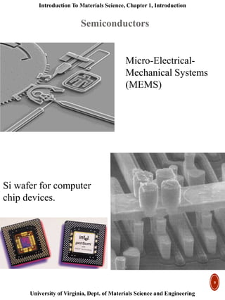
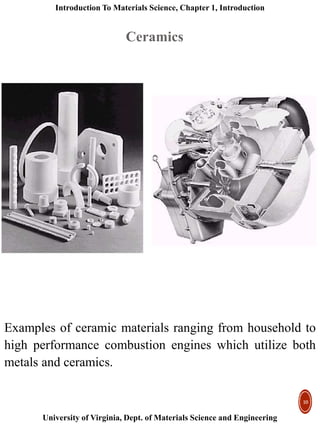
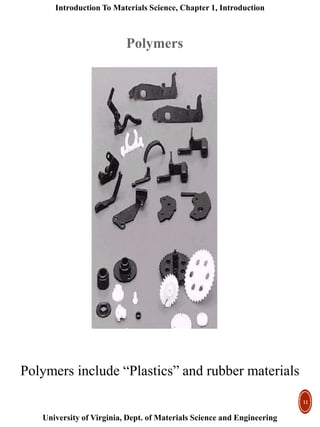
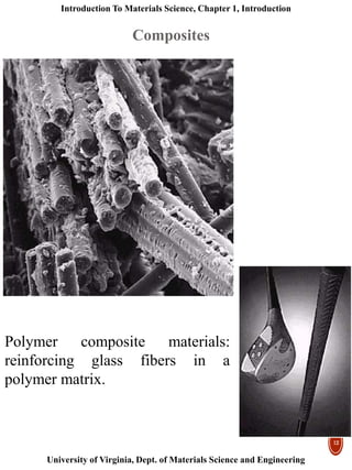
2. Introduction To Materials Science, Chapter 1, Introduction
University of Virginia, Dept. of Materials Science and Engineering
2
• Historical Perspective
Stone Bronze Iron Advanced materials
• What is Materials Science and
Engineering ?
Processing Structure Properties
• Classification of Materials
Metals, Ceramics, Polymers, Semiconductors
• Advanced Materials
Electronic materials, superconductors, etc.
• Modern Material's Needs, Material of
Future
Biodegradable materials, Nanomaterials, “Smart”
materials
Topic Outline
3. Introduction To Materials Science, Chapter 1, Introduction
University of Virginia, Dept. of Materials Science and Engineering
3
• Beginning of the Material Science - People began to
make tools from stone – Start of the Stone Age about
two million years ago.
Natural materials: stone, wood, clay, skins, etc.
• The Stone Age ended about 5000 years ago with
introduction of Bronze in the Far East. Bronze is an
alloy (a metal made up of more than one element),
copper + < 25% of tin + other elements.
Bronze: can be hammered or cast into a variety of
shapes, can be made harder by alloying, corrode only
slowly after a surface oxide film forms.
• The Iron Age began about 3000 years ago and continues
today. Use of iron and steel, a stronger and cheaper
material changed drastically daily life of a common
person.
• Age of Advanced materials: throughout the Iron Age
many new types of materials have been introduced
(ceramic, semiconductors, polymers, composites…).
Understanding of the relationship among structure,
properties, processing, and performance of materials.
Intelligent design of new materials.
Historical Perspective
4. Introduction To Materials Science, Chapter 1, Introduction
University of Virginia, Dept. of Materials Science and Engineering
4
• Subatomic level
Electronic structure of individual atoms
that defines interaction among atoms
(interatomic bonding).
• Atomic level
Arrangement of atoms in materials (for
the same atoms can have different
properties, e.g. two forms of carbon:
graphite and diamond)
• Microscopic structure
Arrangement of small grains of material
that can be identified by microscopy.
• Macroscopic structure
Structural elements that may be viewed
with the naked eye.
Structure
Annealing of a polycrystalline grain structure
2D simulation using Monte Carlo Potts model.
2D simulations involve 40,000 sites and takes a day to run on a fast
workstation, 3D simulations involve 64 million sites, runs on 1000
processors of ASCI-Red.
Monarch butterfly
~ 0.1 m
5. Introduction To Materials Science, Chapter 1, Introduction
University of Virginia, Dept. of Materials Science and Engineering
5
Material science is the investigation of the relationship
among processing, structure, properties, and
performance of materials. The combination of physics,
chemistry, and the focus on the relationship between
the properties of a material and its microstructure is
the domain of Materials Science.
What is Materials Science and Engineering ?
Processing
PropertiesStructure
Observational
Materials
Optimization Loop
6. Introduction To Materials Science, Chapter 1, Introduction
University of Virginia, Dept. of Materials Science and Engineering
6
Properties are the way the material responds to the
environment and external forces.
Mechanical properties – response to mechanical forces,
strength, etc.
Electrical and magnetic properties - response electrical
and magnetic fields, conductivity, etc.
Thermal properties are related to transmission of heat and
heat capacity.
Optical properties include to absorption, transmission and
scattering of light.
Chemical stability in contact with the environment -
corrosion resistance.
Properties
7. Introduction To Materials Science, Chapter 1, Introduction
University of Virginia, Dept. of Materials Science and Engineering
7
Types of Materials
Let us classify materials according to the way the atoms are
bound together.
Metals: valence electrons are detached from atoms, and
spread in an 'electron sea' that "glues" the ions together.
Strong, ductile, conduct electricity and heat well, are shiny
if polished.
Semiconductors: the bonding is covalent (electrons are
shared between atoms). Their electrical properties depend
strongly on minute proportions of contaminants. Examples:
Si, Ge, GaAs.
Ceramics: atoms behave like either positive or negative
ions, and are bound by Coulomb forces. They are usually
combinations of metals or semiconductors with oxygen,
nitrogen or carbon (oxides, nitrides, and carbides). Hard,
brittle, insulators. Examples: glass, porcelain.
Polymers: are bound by covalent forces and also by weak
van der Waals forces, and usually based on C and H. They
decompose at moderate temperatures (100 – 400 C), and
are lightweight. Examples: plastics rubber.
8. Introduction To Materials Science, Chapter 1, Introduction
University of Virginia, Dept. of Materials Science and Engineering
8
Several uses of steel and
pressed aluminum.
Metals
9. Introduction To Materials Science, Chapter 1, Introduction
University of Virginia, Dept. of Materials Science and Engineering
9
Si wafer for computer
chip devices.
Semiconductors
Micro-Electrical-
Mechanical Systems
(MEMS)
10. Introduction To Materials Science, Chapter 1, Introduction
University of Virginia, Dept. of Materials Science and Engineering
10
Examples of ceramic materials ranging from household to
high performance combustion engines which utilize both
metals and ceramics.
Ceramics
11. Introduction To Materials Science, Chapter 1, Introduction
University of Virginia, Dept. of Materials Science and Engineering
11
Polymers include “Plastics” and rubber materials
Polymers
12. Introduction To Materials Science, Chapter 1, Introduction
University of Virginia, Dept. of Materials Science and Engineering
12
Polymer composite materials:
reinforcing glass fibers in a
polymer matrix.
Composites
13. Introduction To Materials Science, Chapter 1, Introduction
University of Virginia, Dept. of Materials Science and Engineering
13
Different materials exhibit different crystal structures
and resultant Properties
(a) (b)
force
Material Selection
14. Introduction To Materials Science, Chapter 1, Introduction
University of Virginia, Dept. of Materials Science and Engineering
14
Different materials exhibit different microstructures
(Chapter 4) and resultant Properties
Material Selection
Superplastic deformation involves low-stress sliding along
grain boundaries, a complex process of which material
scientists have limited knowledge and that is a subject of
current investigations.
15. Introduction To Materials Science, Chapter 1, Introduction
University of Virginia, Dept. of Materials Science and Engineering
15
How do you decide on a specific material for your
application ?
Material Selection
16. Introduction To Materials Science, Chapter 1, Introduction
University of Virginia, Dept. of Materials Science and Engineering
16
Composition, Bonding, Crystal Structure
and Microstructure DEFINE Materials Properties
Composition
Bonding Crystal Structure
Thermomechanical
Processing
Microstructure
17. Introduction To Materials Science, Chapter 1, Introduction
University of Virginia, Dept. of Materials Science and Engineering
17
Design of materials having specific desired characteristics
directly from our knowledge of atomic structure.
• Miniaturization: “Nanostructured" materials, with
microstructure that has length scales between 1 and 100
nanometers with unusual properties. Electronic
components, materials for quantum computing.
• Smart materials: airplane wings that deice themselves,
buildings that stabilize themselves in earthquakes…
• Environment-friendly materials: biodegradable or
photodegradable plastics, advances in nuclear waste
processing, etc.
• Learning from Nature: shells and biological hard tissue
can be as strong as the most advanced laboratory-produced
ceramics, mollusces produce biocompatible adhesives that
we do not know how to reproduce…
• Materials for lightweight batteries with high storage
densities, for turbine blades that can operate at 2500°C,
room-temperature superconductors? chemical sensors
(artificial nose) of extremely high sensitivity, cotton shirts
that never require ironing…
Future of materials science