- The document discusses carrier action in semiconductors including drift, diffusion, and recombination-generation of carriers.
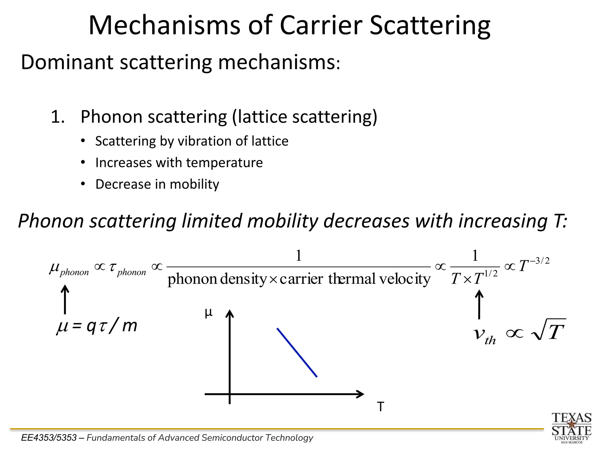
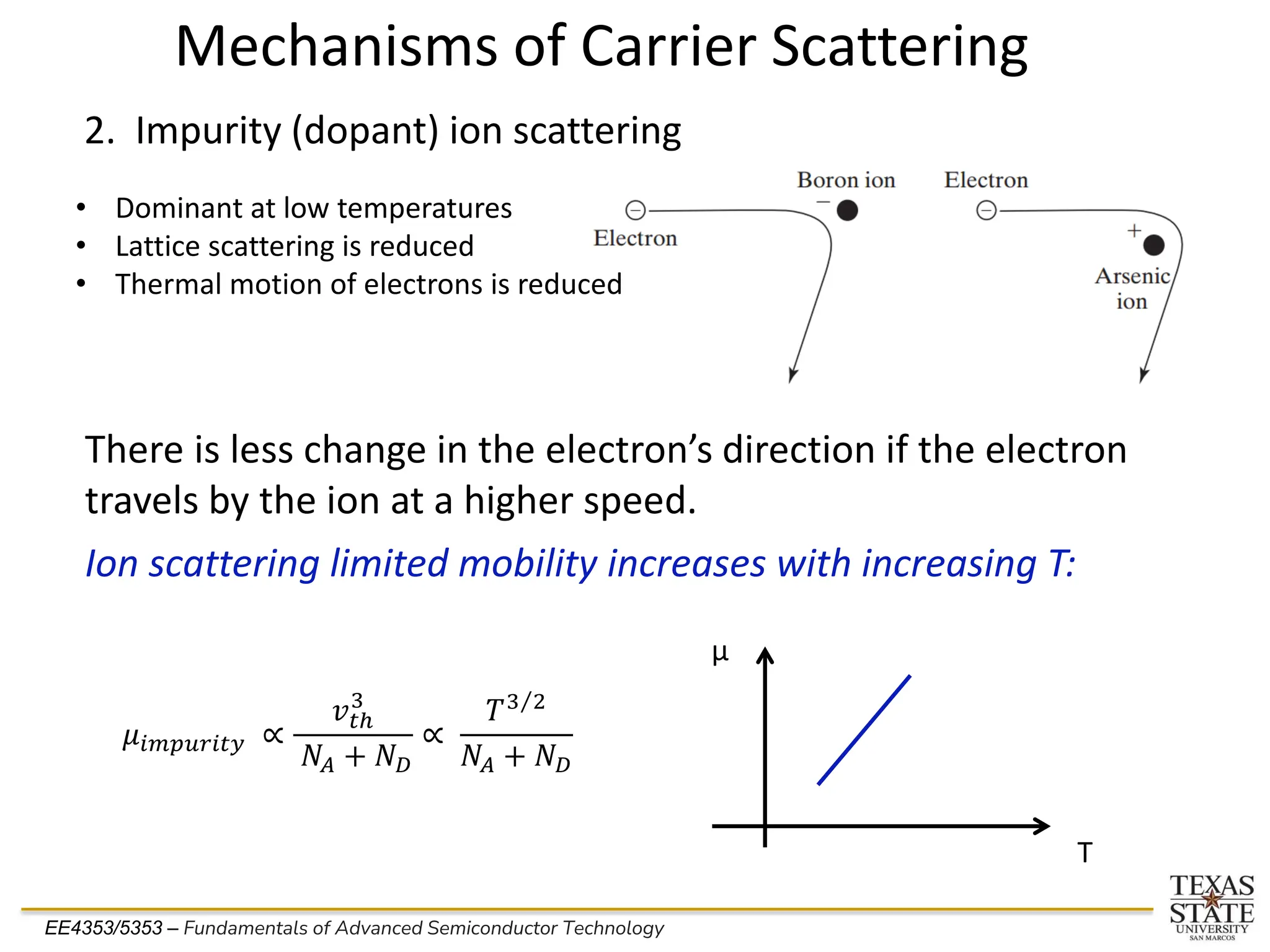
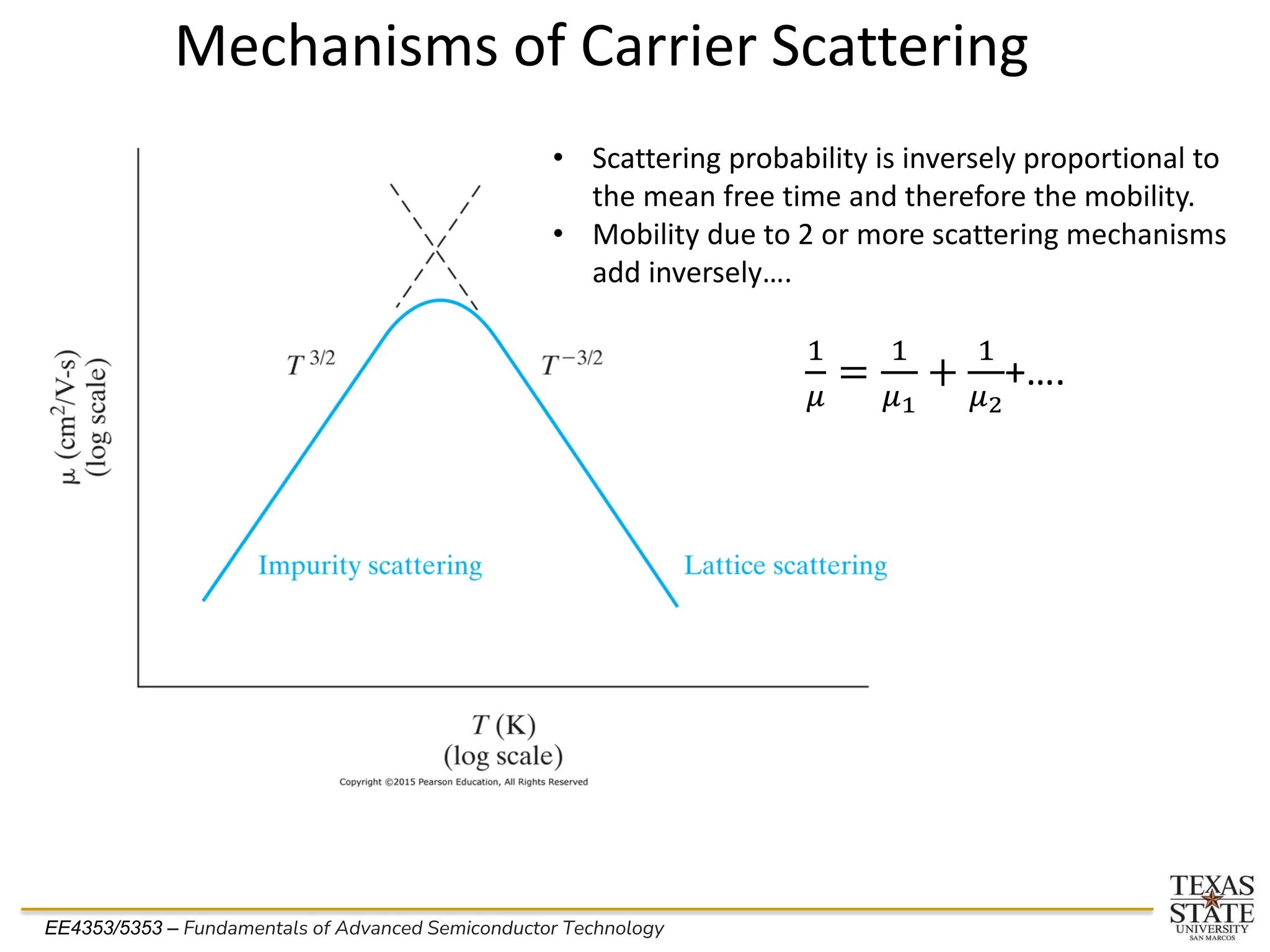
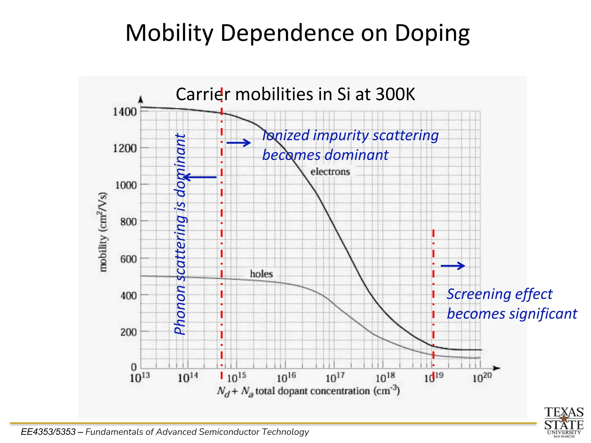
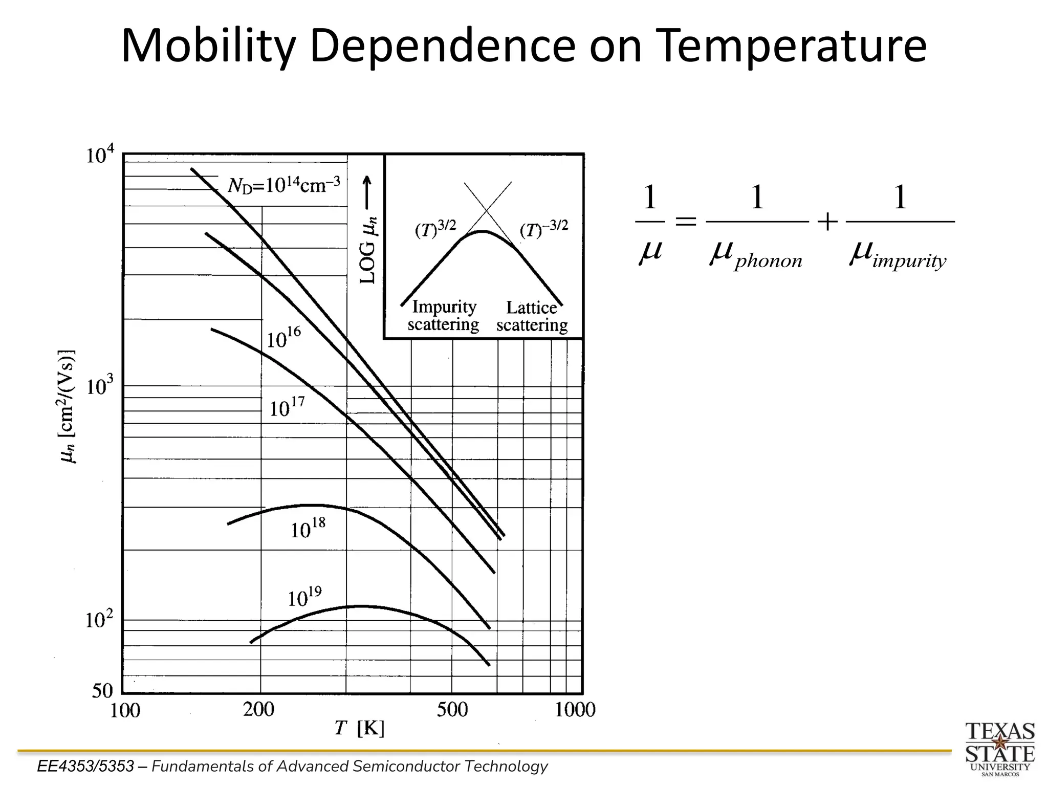
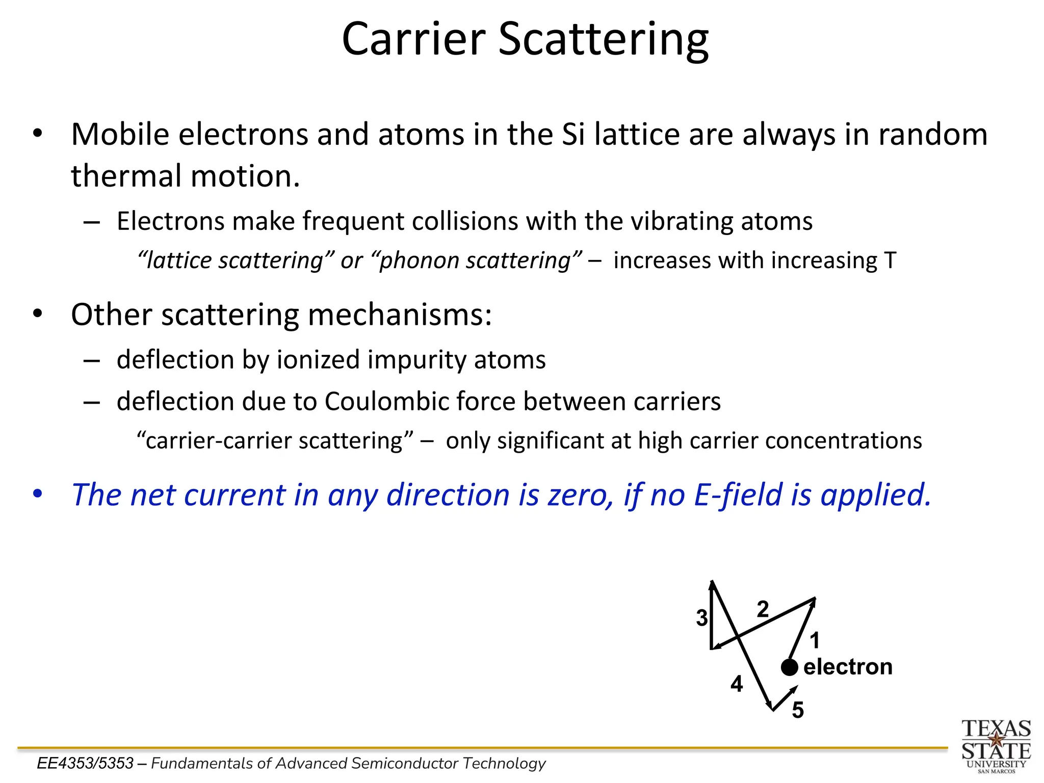
- It describes carrier scattering mechanisms such as phonon scattering and impurity scattering. Carrier mobility is defined and its dependence on temperature and doping is explained.
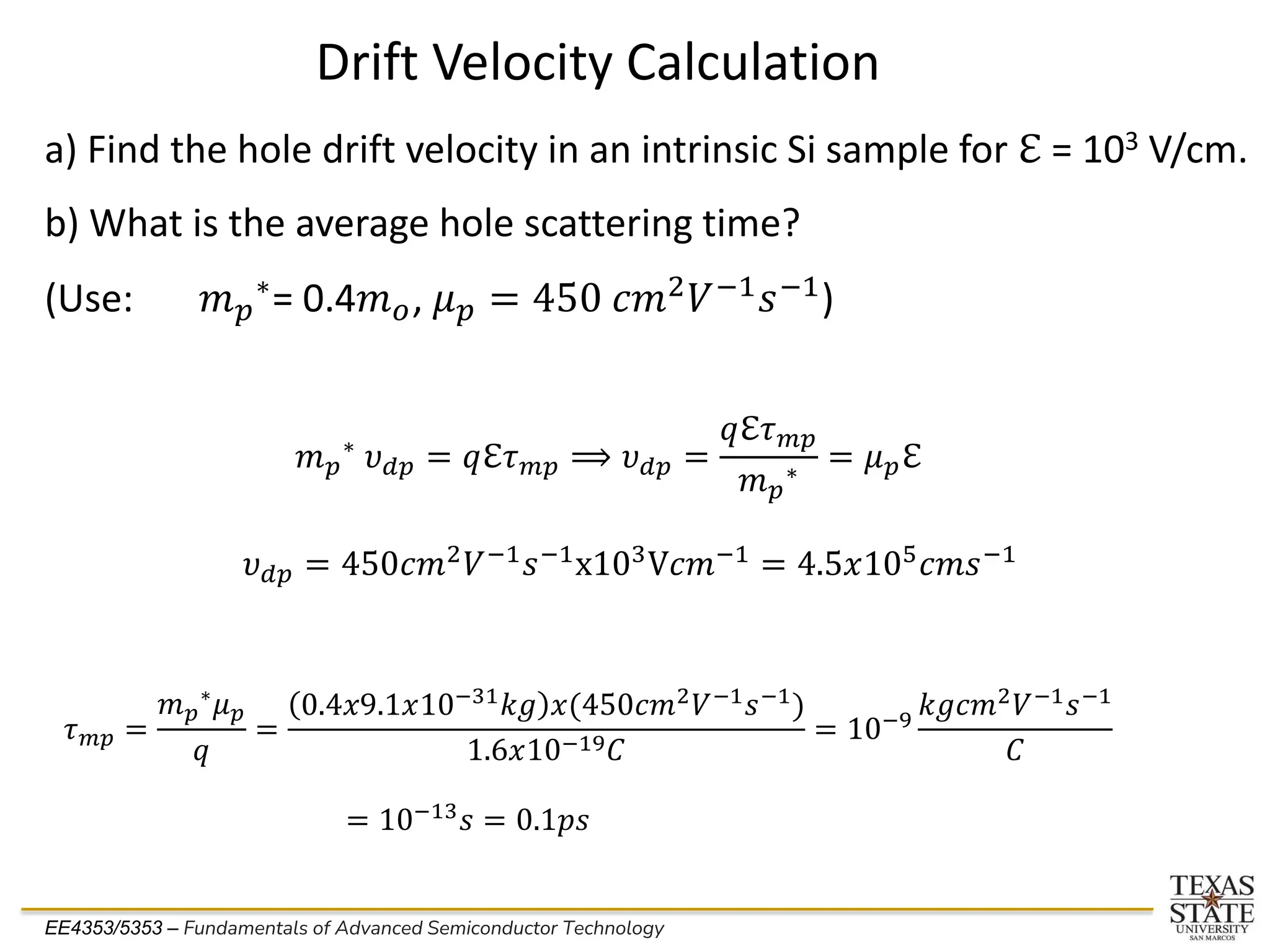
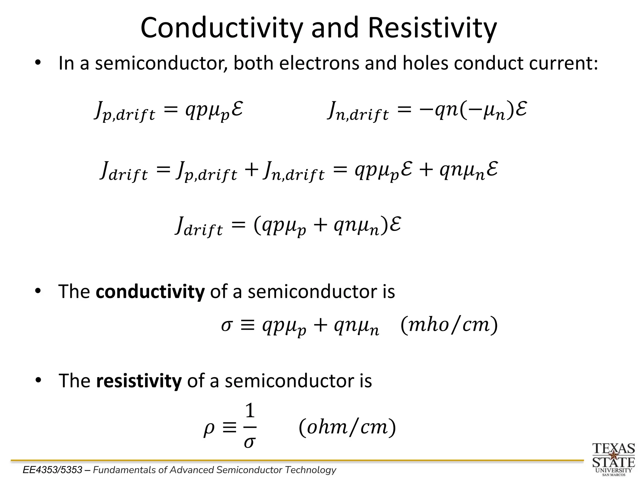
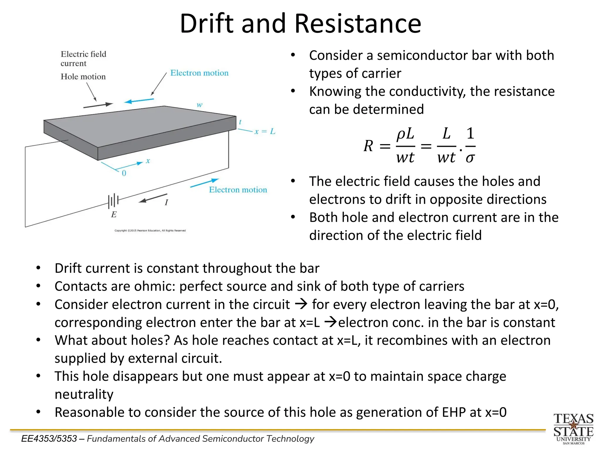
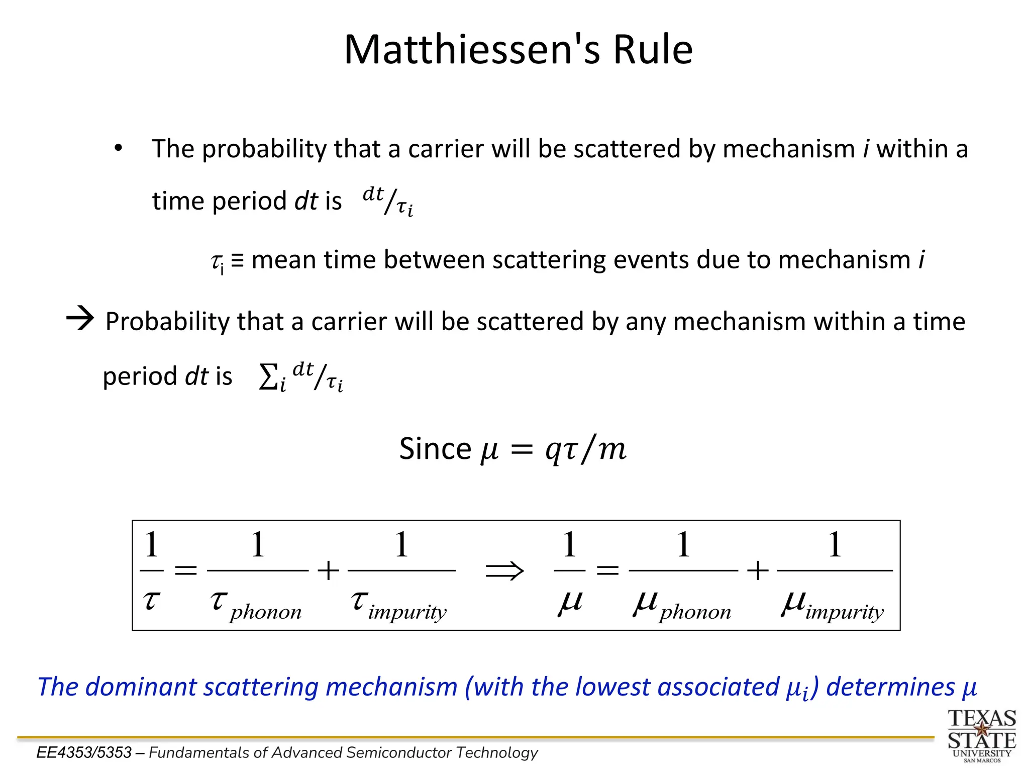
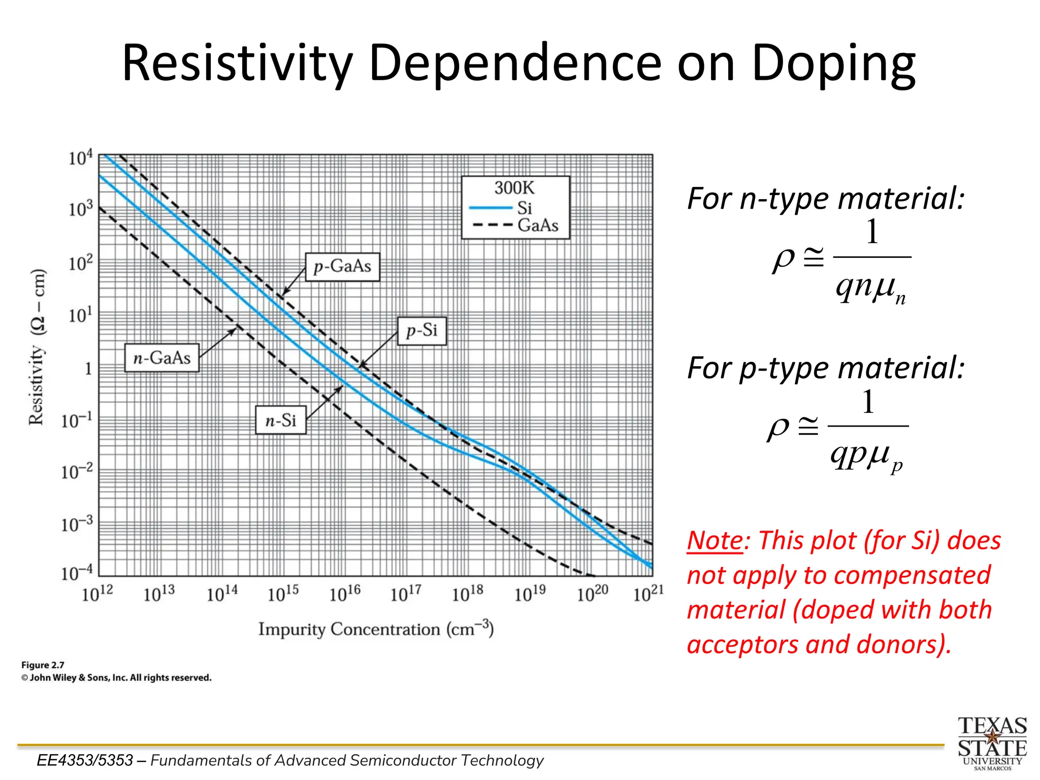
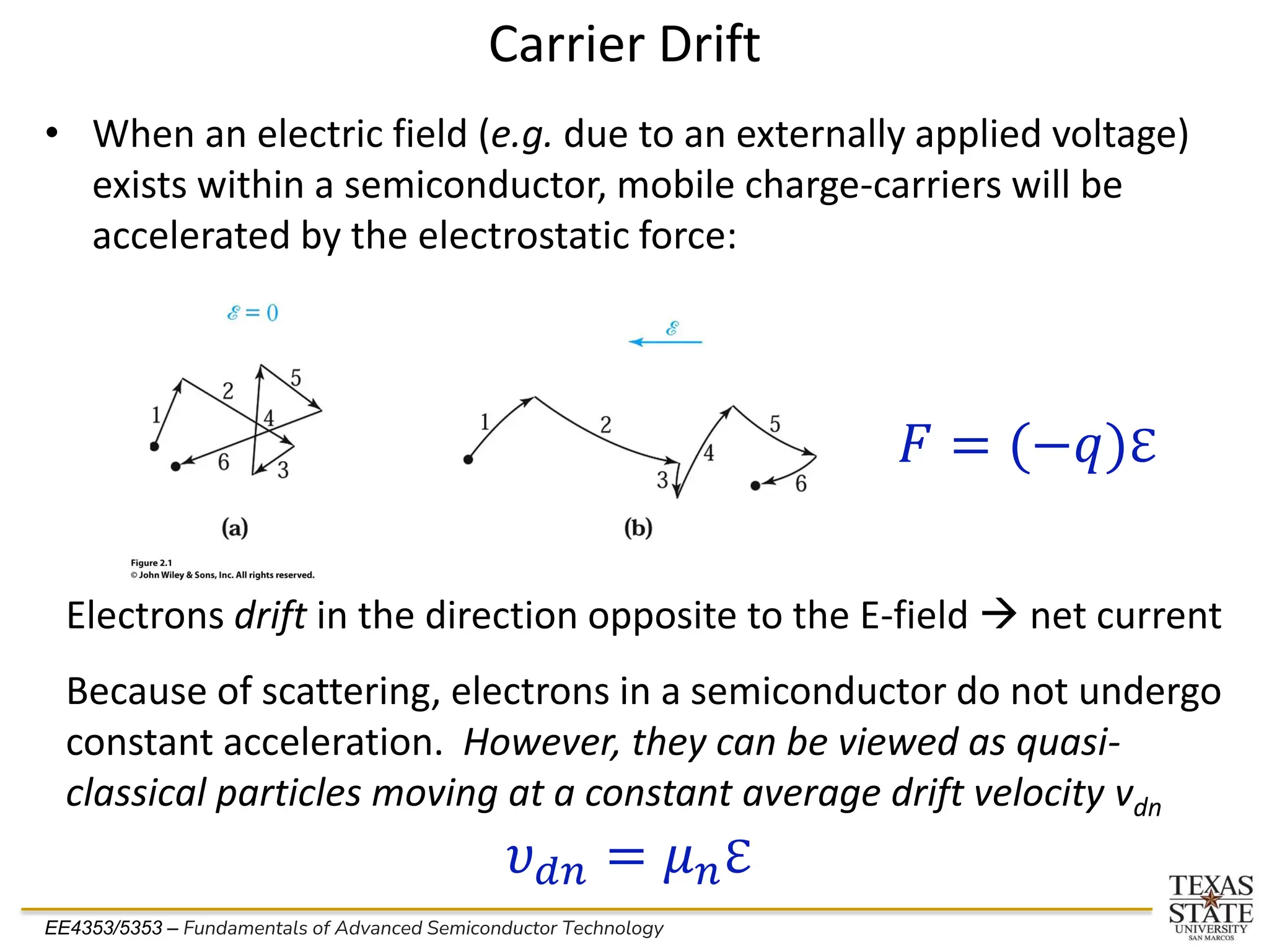
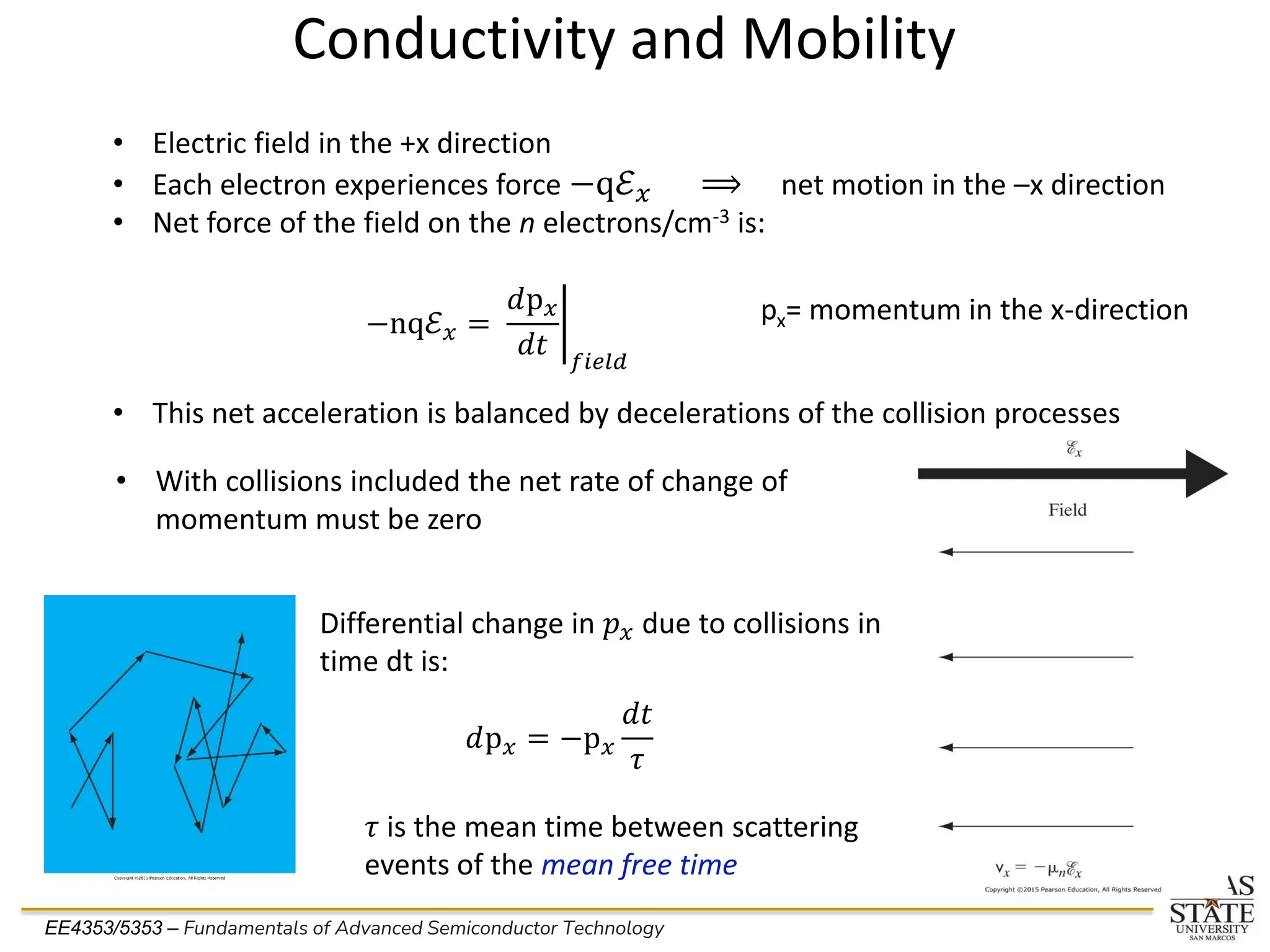
- The concepts of conductivity, resistivity, and drift velocity are introduced. Matthiessen's rule for combining scattering mechanisms is also covered.
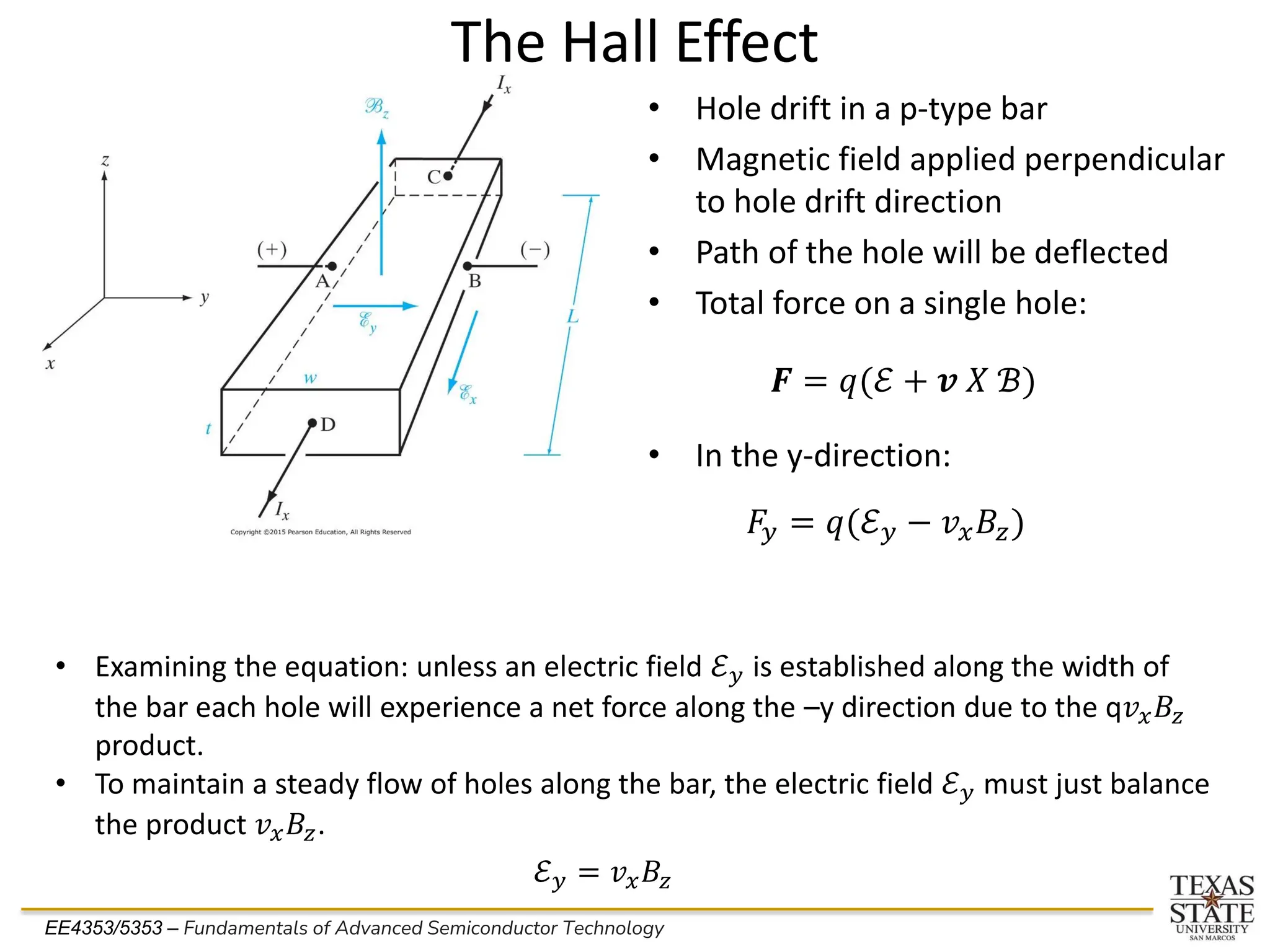
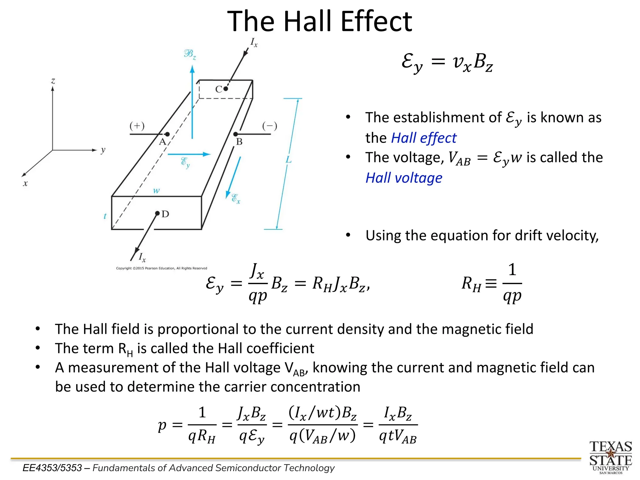
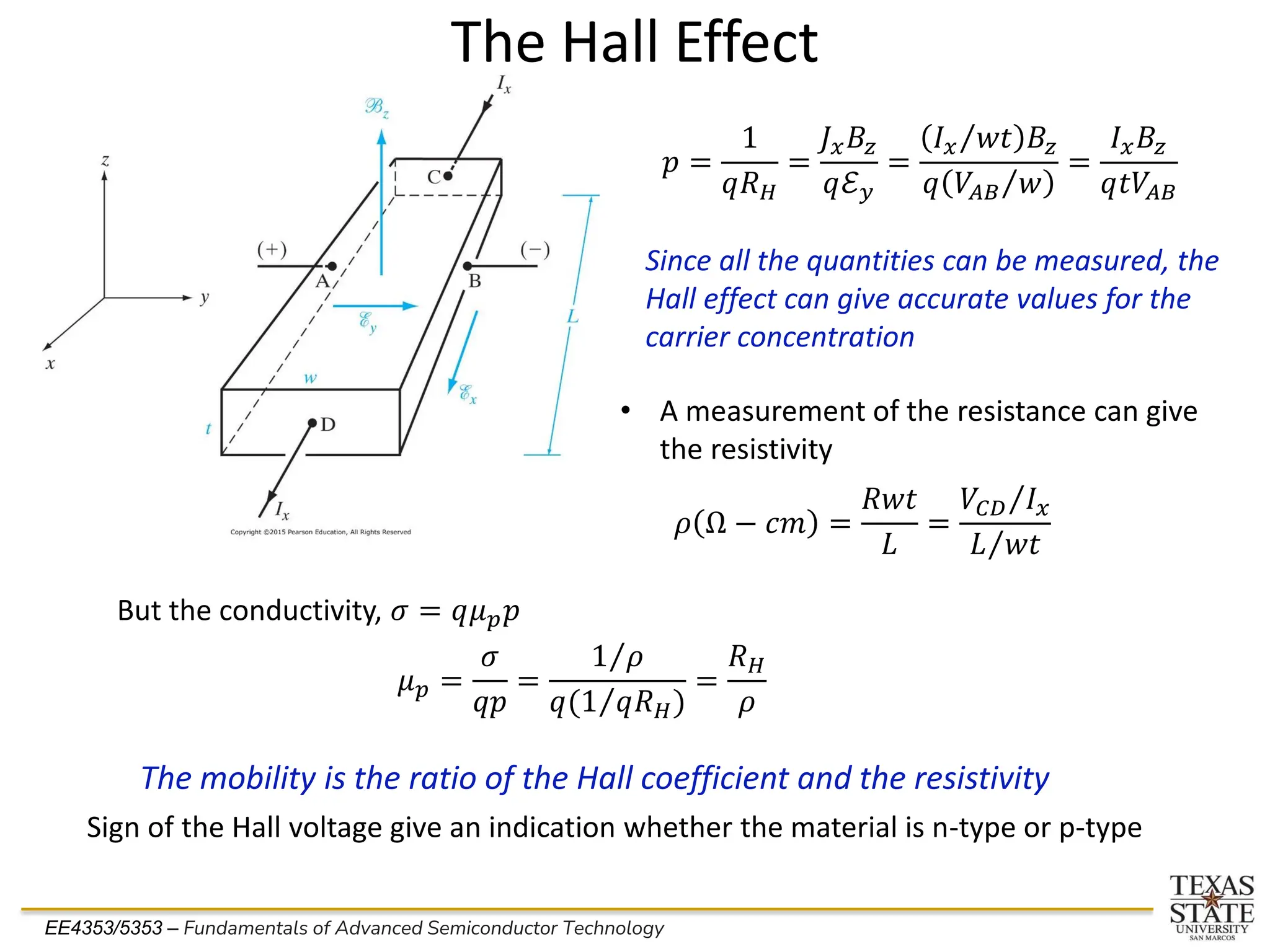
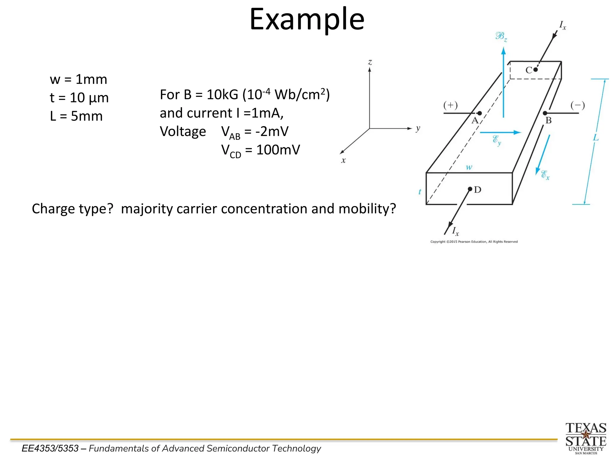
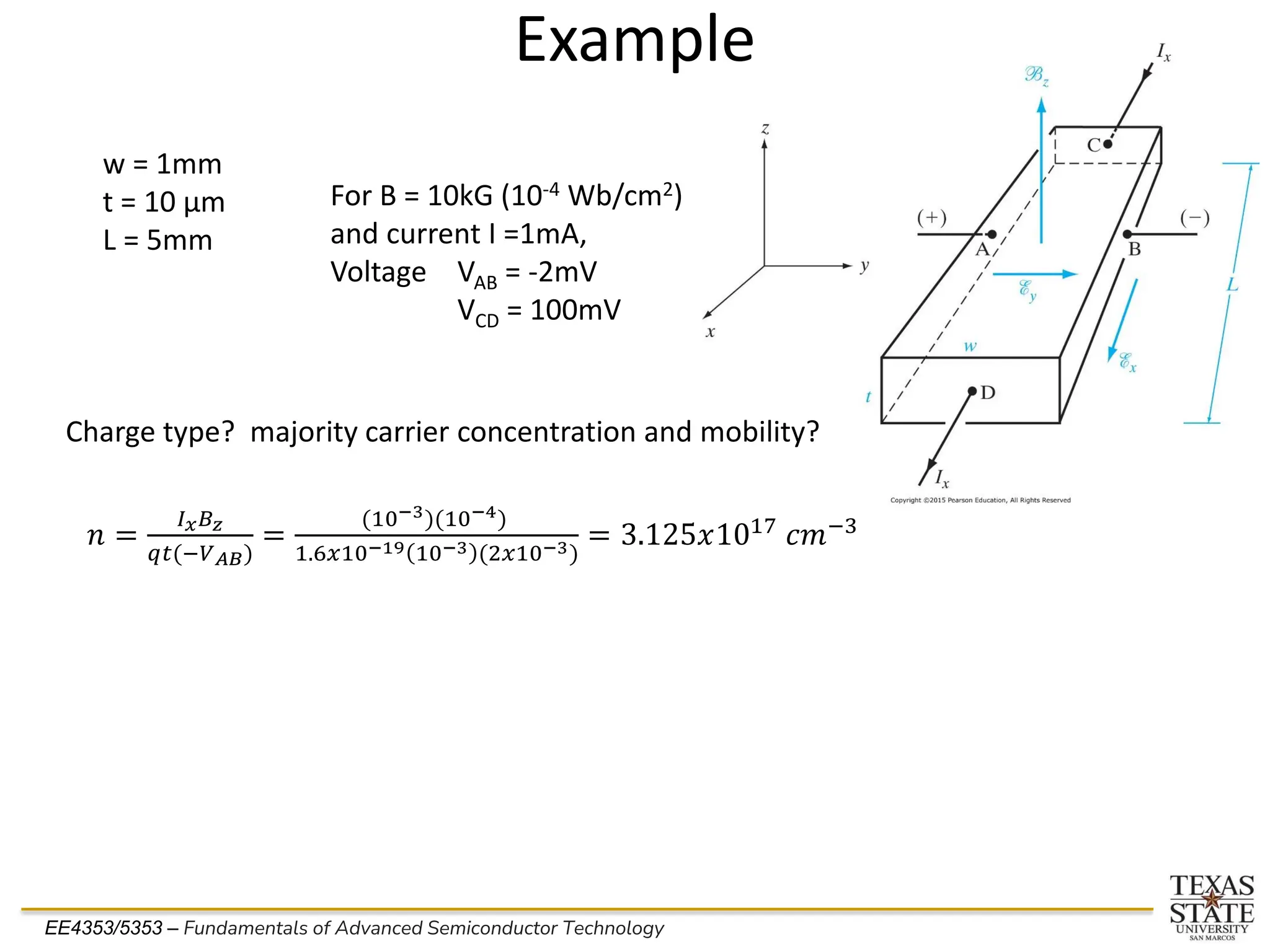
- Finally, the Hall effect is summarized as the establishment of an electric field perpendicular to the direction of carrier drift in the presence of a magnetic field.
![EE4353/5353 – Fundamentals of Advanced Semiconductor Technology
Carrier Mobility, m
mn [qtmn / mn*] is the electron mobility
mp [qtmp / mp*] is the hole mobility
Similarly, for holes:
Si Ge GaAs InAs
mn (cm2/Vs) 1400 3900 8500 30,000
mp (cm2/Vs) 450 1900 400 500
Electron and hole mobilities for intrinsic semiconductors @ 300K
For electrons:
𝜐𝑑𝑝 = ൘
𝑞ℇ𝜏𝑚𝑝
𝑚𝑝
∗ ≡ 𝜇𝑝ℇ
𝜐𝑑𝑛 = ൗ
𝑞ℇ𝜏𝑚𝑛
𝑚𝑛
∗ ≡ 𝜇𝑛ℇ](https://image.slidesharecdn.com/l-04-carrieraction-240416203525-77fbb3f7/75/The-carrier-structure-of-a-P-and-N-type-Semiconductor-7-2048.jpg)