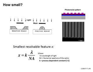
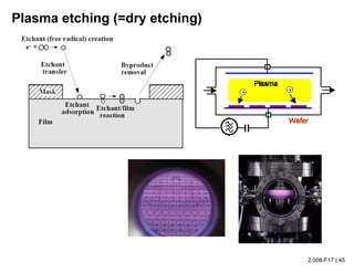
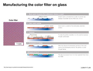
2.008-F17 | 1
Manufacturing of electronics
MIT 2.008 – Prof. John Hart
November 29, 2017
2.008-F17 | 2
LCD Touch
Screen
Front Case
Battery
Circuit board
Back Case
2.008-F17 | 3
Speaker
Back Camera
WiFi
Antenna
Headset Connector
Processor etc
(shielded)
2.008-F17 | 4
Flash memory
(8 GB)
CPU (Quad-core
ARM 1.3 GHz)
2.008-F17 | 5
2.008-F17 | 6
11 W power, 815 lumens
25,000 hours
$5.99
60 W power, 590 lumens
2,000 hours
~$0.60
Light bulbs: old and new
2.008-F17 | 7
2.008-F17 | 8
Key manufacturing technologies for electronic
products
§ Integrated circuit (IC) processing (i.e., ‘semiconductor
manufacturing) à often done on silicon wafers to achieve
high density circuits. This includes (with ~nm precision):
§ Thin film deposition
§ Photolithography (patterning, like each layer of SLA)
§ Etching
§ Planarization (polishing)
§ Circuit board manufacturing and soldering à to hold
the ICs and create custom electronic systems
§ Pick-and-place assembly à packaging ICs and other
components; placing components on circuit boards
§ Connectors (rigid and flexible) à connect rigid boards to
buttons, batteries, antennas, etc.
§ Emerging technologies including fully printed devices.
2.008-F17 | 9
Inside the integrated circuit (IC)
http://electronics.stackexchange.com/questions/56649/what-is-a-die-package
Gold wire connections to
the chip circuitry
2.008-F17 | 10
Inside the integrated circuit (IC)
Slide adapted from E. Pop
2.008-F17 | 11
Building block: MOSFET transistor
Image: E. Pop
Textbook: Prof. Chenming Hu, http://www.eecs.berkeley.edu/~hu/
Video on how transistors work: http://www.youtube.com/watch?v=IcrBqCFLHIY
2.008-F17 | 12
Approaching atomic resolution
2.008-F17 | 13
John Bardeen, William Shockley
and Walter Brattain at Bell Labs,
1948.
The first transistor
Gate
Book: “The Idea Factory: Bell Labs and the Great
Age of American Innovation”
2.008-F17 | 14
Platform: silicon wafers
2.008-F17 | 15Intel.
2.008-F17 | 16
Moore’s law: number of transistors on a chip
~doubles every two years
http://en.wikipedia.org/wiki/Moore's_law; https://en.wikipedia.org/wiki/Transistor_count
2016: Apple A10
(iPhone 7) has 3.3
billion transistors over
an area of 125 mm2
.
à Effective cost of
one transistor is less
than one letter printed
in the newspaper!
($ ~0.1x10⁻⁶)
2.008-F17 | 17
A semiconductor manufacturing plant
http://www.samsung.com/global/business/semiconductor/foundry
/manufacturing/overview
2.008-F17 | 18
The semiconductor plant (‘fab’)
§ Worldwide, >170 major semiconductor manufacturing plants.
§ Cost per plant >$1 BILLION.…can easily reach $3-4 billion.
Samsung spent $14.7 billion USD on their new memory chip
plant (2014).
§ The central part of a semiconductor plant is the clean room
§ Eliminate ~all dust, temperature and humidity control to minimize static
electricity, dampened against vibration.
§ Machines to be found in the clean room are steppers for photolithography,
etching, cleaning, doping and dicing machines. The typical price range for
new machines is $700,000 to $4,000,000 ..and up to $50,000,000 for each
wafer stepper. Hundreds of machines are needed in one plant.
§ The capital depreciation can account for 50-80% of
manufacturing cost! Thus semiconductor manufacturing
equipment has a large secondary market.
http://www.ft.com/cms/s/0/b478b190-4d03-11e4-a0d7-00144feab7de.html#axzz3KbtVQwYG
http://en.wikipedia.org/wiki/Semiconductor_fabrication_plant
http://www.forbes.com/sites/jimhandy/2011/12/19/whats-it-like-in-a-semiconductor-fab/
2.008-F17 | 19
Layout of a semiconductor fab
‘Front-end’
‘Back-end’
Image from FormFactor:
http://www.sec.gov/Archives/edgar/data/1039399/000089161803002980/f80848b1f80848f2.gif
2.008-F17 | 20
MIT.nano (2018)
mitnano.mit.edu
2.008-F17 | 21
Generic device fabrication
Blank Si wafer
Material addition or
removal
(Characterization)
Complete device
Final
test
Material addition
• Chemical or physical
vapor deposition
(PVD or CVD)
• Oxidation
• Doping
• Ion implantation
• Electroplating
Next step?
Material removal
• Wet etching
• Dry (gas/plasma)
etching
• Chemical/mechanical
polishing (CMP)
Pattern transfer
(lithography)
2.008-F17 | 22S. Bathhurst / S.G. Kim, MIT
Silicon wafer production
Si ingot (single
crystal)
Wafers (up to 300
mm diameter)
Slicing: rotating saw or
abrasive-coated wire.
Then: etching/polishing surface.
Key specs: thickness,
roughness, flatness (“wafer
bow”)
2.008-F17 | 23
2.008-F17 | 24
Example: building an array of interconnects (wires)
à W ~20 nm; t ~5 nm
Si wafer
SiO2
Metal
2.008-F17 | 25
Si wafer
Si wafer
SiO2
Deposit or ‘grow’ SiO2 layer
Begin with bare Si wafer (polished surface)
Deposit metal layer
Metal
Coat photoresist (PR)
Photoresist
Pattern photoresist (this is photolithography)
Etch metal (using patterned PR as the mask)
Remove photoresist
Si wafer
SiO2
Metal
2.008-F17 | 26
Thin film deposition methods
§ Surface reaction: the surface of the wafer
reacts to form a thin film; for example,
oxidation. The substrate surface is
consumed.
§ Physical vapor deposition (PVD): a film
is created by exposing the substrate
(lower temp) to a vapor of the desired
material.
§ Chemical vapor deposition (CVD): a film
is created by a chemical reaction of
gaseous precursors at the substrate
surface (but not consuming the substrate).
PVD by
evaporation
2.008-F17 | 27
Chemical vapor deposition (CVD)
2.008-F17 | 28
Chemical vapor deposition (CVD)
§ CVD: deposits a thin film from gaseous precursors via a
chemical reaction at the surface of a substrate.
§ Example materials:
§ Dielectrics: SiO2, Si3N4.
§ Metals: W, Al, others.
§ Semiconductors: Si, GaAs.
§ Versatile, conformal (coats topography)
§ Crystal structure of film can be controlled by process and/or
interactions with substrate.
from J. Chun
2.008-F17 | 29
CVD process physics: deposition of SiO2
1,7 : Diffusion 2-6 : Reactions
Generic: 2AB (gas) → 2A (solid) + B2 (gas)
Ex. http://www-inst.eecs.berkeley.edu/~ee143/fa10/lectures/Lec_13.pdf
2.008-F17 | 30http://www.mdpi.com/sensors/sensors-13-09513/article_deploy/html/images/sensors-13-09513f4-1024.png
2.008-F17 | 31
CVD: parameters
from J. Chun; http://www-inst.eecs.berkeley.edu/~ee143/fa10/lectures/Lec_13.pdf
Process parameters
§ Temperature
§ Total pressure
§ Partial pressure of reactants
§ Flow rate of reactants and
carrier gases
§ Time
Control parameters
§ Film thickness (~1-1000 nm,
getting thinner à atomic layers)
§ Film deposition rate (~nm/s)
§ Film uniformity and quality
Rate ∝e
−
Ea
kT
Log(rate)
High T Low T
Rate ∝T3/2
2.008-F17 | 32
CVD: quality
§ Conformal coverage
: For deep submicron devices, the step
coverage of films into high aspect ratio
features is extremely difficult.
§ Voids
: If deposition rate is too high,
voids may be left
from J. Chun
2.008-F17 | 33
Si wafer
Si wafer
SiO2
Deposit or ‘grow’ SiO2 layer
Begin with bare Si wafer (polished surface)
Deposit metal layer
Metal
Coat photoresist (PR)
Photoresist
Pattern photoresist (this is photolithography)
Etch metal (using patterned PR as the mask)
Remove photoresist
Si wafer
SiO2
Metal
2.008-F17 | 34http://commons.wikimedia.org/wiki/File:Spin-coater_for_resist_coating_(DE).svg
Photoresist spin-coating
2.008-F17 | 35http://www.lithoguru.com/scientist/lithobasics.html
t ~ µ1/3
ω−1/2
2.008-F17 | 36
Si wafer
Si wafer
SiO2
Deposit or ‘grow’ SiO2 layer
Begin with bare Si wafer (polished surface)
Deposit metal layer
Metal
Coat photoresist (PR)
Photoresist
Pattern photoresist (this is photolithography)
Etch metal (using patterned PR as the mask)
Remove photoresist
Si wafer
SiO2
Metal
2.008-F17 | 37
Photolithography: pattern transfer to the wafer
(light, UV, X-ray,
e-beam)
Mask (the pattern to
be transferred)
2.008-F17 | 38
Mask patterns = Chrome
Substrate = Glass (soda-lime or quartz)
2.008-F17 | 39
ASML wafer stepper
from J. Chun
Cost: up to $50M for 300mm wafers
Quality: sub-10nm alignment accuracy
Rate: m/s speed.
Flexibility: any mask (but masks are expensive)
2.008-F17 | 40
How small?
Photoresist pattern
Mask
Pattern photoresist (this is photolithography)
Etch metal (using patterned PR as the mask)
Remove photoresist
Si wafer
SiO2
Metal
Light
k	=	process-dependent	constant	(<1)
2.008-F17 | 41
Shrinking circuits with water:
http://www.nature.com/scientificamerican/journal/v293/n1/full/scie
ntificamerican0705-64.html
2.008-F17 | 42
Pattern photoresist (this is photolithography)
Etch metal (using patterned PR as the mask)
Remove photoresist
Si wafer
SiO2
Metal
à ‘Dry’ etching (gas or plasma) or ‘Wet’ etching (liquid)
Important:
§ Selectivity of material to be etched vs mask
§ Degree of directionality (anisotropy)
Last, etching
2.008-F17 | 43
Etching
2.008-F17 | 44
Etching
Low selectivity
High selectivity
2.008-F17 | 45
Plasma etching (=dry etching)
2.008-F17 | 46
Etch metal (using patterned PR as the mask)
Remove photoresist
Si wafer
SiO2
Metal
What is important for high
quality fabrication of each layer?
§ …
§ …
2.008-F17 | 47
Reflection: semiconductor manufacturing
§ Rate?
§ Quality?
§ Cost?
§ Flexibility?
à How do these answers influence how electronic
products are designed and manufactured?
2.008-F17 | 48
Generic process flow
Blank Si wafer
Material addition or
removal
(Characterization)
Complete device
Final
test
Material addition
• Chemical or physical
vapor deposition
(PVD or CVD)
• Oxidation
• Doping
• Ion implantation
• Electroplating
Next step?
Material removal
• Wet etching
• Dry (gas/plasma)
etching
• Chemical/mechanical
polishing (CMP)
Pattern transfer
(lithography)
2.008-F17 | 49
(part 2)
2.008-F17 | 50
3D transistors: Intel “FINFET”
22 nm refers to the half-pitch of the pattern, thus one transistor every 44 nm
https://www.semiwiki.com/forum/content/1709-designing-finfets.html
2.008-F17 | 51
The smallest transistor gate yet (UC Berkeley, 2016)
MoS2 transistors with 1-nanometer gate lengths; http://science.sciencemag.org.libproxy.mit.edu/content/354/6308/99
https://www.sciencedaily.com/releases/2016/10/161006140546.htm
2.008-F17 | 52
Digital light projector (DLP): micromirror array!
à Texas Instruments invented 1987, first product shipped 1996
à Now arrays of >2 million (~2000x1000) mirrors each ~5x5 um!
Texas Instruments /
http://www.memsjournal.com/2013/02/mems-based-optical-
engine-platforms-market-and-technology-overview.html
2.008-F17 | 53
2.008-F17 | 54
§ Hinges: 60x600 nm, flex ±10°
§ The hinges have ~infinite fatigue life*
because their size along with the thin
film process control makes them single
crystals!!
*Array verified to 3 x 10¹² cycles = 120 years life at 1000 hours per year.à 14 x 1018
individual mirror cycles without a single hinge fatigue failure!
2.008-F17 | 55
Mirror lifetime
Douglas, Proceedings of the SPIE, 4980:1-11, 2003.
§ Verified to 3 x 10¹² cycles = 120 years life at 1000 hours
per year.
§ ~1,000,000 mirrors per device à ~1019 individual mirror
cycles without a single hinge fatigue failure!
2.008-F17 | 56
MEMS accelerometer (Analog Devices / Stata)
2.008-F17 | 57
MEMS + electronics: Package with ASIC
(Application-Specific Integrated Circuit)
§ The picture below shows a schematic of a
complete integrated circuit system inside
a package.
§ The upper right picture shows a x-ray
picture of a connected ASIC and MEMS
die with a hermetic cap.
§ The lower right picture shows an SEM
picture of the same device with the cap
removed.
Also see ST Microelectronics
http://electronics.stackexchange.com/questions/51441/how-thick-or-thin-is-the-die-wafer-inside-an-ic
http://www.elmos.com/english/products/know-how/system-in-a-package.html
2.008-F17 | 58
Transistors and MEMS are complicated and
sophisticated
…but uniform thin films and simple
photolithography patterns are extremely relevant
and useful!
(and also very sophisticated)
2.008-F17 | 59
Amazon Fire LCD display
Color filter
(rotated 45 deg)
1 mm
LCD
Display
Front Case
LCD display
Glass + touch sensors
2.008-F17 | 60
Manufacturing the color filter on glass
http://www.toppan.co.jp/electronics/english/display/lcd/production/
Color filter
1 mm
2.008-F17 | 61
Capacitive touch screen
1. Touchscreens 101: Understanding Touchscreen Technology and Design By Steve Kolokowsky, Senior Elect Design Engineer, and Trevor Davis, Senior Business
Development Manager, Cypress Semiconductor Corp.
2. Capacitive Touch Sensors Application Fields, technology overview and implementation example: Fujitsu microelectronics group
§ Indium tin oxide (ITO) electrode
pattern is deposited by
photolithography.
§ The touchscreen detects the
change in capacitance as your
finger passes over patterned ITO
electrodes.
§ Glass substrates are bonded by
pressure-sensitive adhesives.
2.008-F17 | 62
ITO: transparency and conductivity
2.008-F17 | 63
Continuous sputtering line
2.008-F17 | 64
2.008-F17 | 65
Flash memory
(8 GB)
CPU (Quad-core
ARM 1.3 GHz)
(part 3 of 3)
2.008-F17 | 66
2.008-F17 | 67
11 W power, 815 lumens
25,000 hours
$5.99
CREE LED light bulb
2.008-F17 | 68
Circuit board (PCB) manufacturing
Circuit board assembly including solder reflow
New pick-and-place technologies
Flexible and 3D circuits
2.008-F17 | 69
What is a circuit board made of?
§ Base board: typically an epoxy-impregnated glass fiber
sheet (e.g., ‘FR-4’).
§ Conductive traces: thin Cu foil (~0.001”), typically made by
rolling or continuous electroplating, then laminated onto the
board, then patterned by photolithography.
§ Components: pin-in-hole (PIH), surface mount (SMT); wide
range of sizes and functionalities.
§ Other features, e.g., alignment holes, insertion holes, vias.
Depends on complexity of the board (single-layer, multi-
layer, etc).
2.008-F17 | 70https://courses.cs.washington.edu/courses/cse467/04wi/lectures/ppt/Intro_to_SMT.pdf
2.008-F17 | 71
Single vs. multilayer PCBs
2.008-F17 | 72Groover.
May have dedicated ground, power planes; placement of
these and coupling (inductive, capacitive) between signal,
ground, power are critical to PCB performance
2.008-F17 | 73
2.008-F17 | 74
PCB manufacturing steps (generic, 2-layer)
§ AOI = automated optical inspection
§ PTH = plated through holes
§ Legend = printing numbers for component placement
§ FQC/A = final quality control/assurance
http://www.pa-international.com/products/pcb-and-pcba
2.008-F17 | 75
Electrodeposition and etching
2.008-F17 | 76
Dry film photoresist: easy to apply to large substrates
2.008-F17 | 77
Stacking a multilayer PCB
https://courses.cs.washington.edu/courses/cse467/04wi/lectures/ppt/Intro_to_SMT.pdf
2.008-F17 | 78http://www.ourpcb.com/multilayer-pcb-5.html
2.008-F17 | 79
Surface mount components on Amazon Fire
Package Dimensions
200 µm
200 µm
Standard SMD
packages
https://en.wikipedia.org/wiki/Surface-
mount_technology
4516
0402
2.008-F17 | 80
Surface mount resistors
http://www.resistorguide.com/thin-and-thick-film/
• Thin film resistive layer is sputtered (vacuum deposition) onto a
ceramic base.
• Thickness ~ 0.1 micrometer (0.0001 mm).
• Resistance value established by photlithography and wet etching
or by laser trimming.
• Higher resistance and high tolerances, low temperature
coefficients and low noise.
• Also for high frequency applications thin film performs better than
thick film. Inductance and capacitance are generally lower.
• Higher cost compared to thick film resistors.
à Thin-film resistive layer
à Thick-film resistive layer
• Thick film resistive layers are deposited by screen printing.
• Thickness ~100 microns (0.1 mm).
• Higher power capacity and lower resistance but low (poor)
tolerance.
• Lower cost.
2.008-F17 | 81
Making surface-mount resistors
https://www.youtube.com/watch?v=wshRwO0MCSU
2.008-F17 | 82
Screen printing
https://www.youtube.com/watch?v=ENJ4FP6C970
Diagram from Kalpakjian; Screen images from Chromaline
§ Mask is typically patterned on the screen
§ Above: ‘325 mesh’ = 44 um opening, woven
stainless steel
§ Screen printing limits ~50-100 um width
and comparable feature height
2.008-F17 | 83
Surface-mount capacitors
KEMET Ceramic Capacitor Manufacturing
(influences capacitance and determines voltage rating)
g
AN
g
A
C
efflayers
ee ==
2.008-F17 | 84
Surface-mount capacitors 1. Screen-printing of electrodes on dielectric
2. Alignment and stacking of layers
including machine vision feedback
3. Singulation and thermal
processing
4. Insertion of chips in a die and
copper terminal coating
5. Electroplating of Ni and Sn on
copper terminals
6. Electrical and optical quality
control inspection
KEMET Ceramic Capacitor Manufacturing
Dielectric
Electrode
2.008-F17 | 85
2.008-F17 | 86
PCB assembly: general sequence
§ Deposit solder paste by screen printing
§ Place components using pick-and-place machine (solder
is a bit sticky)
§ Solder reflow
§ Testing
§ Encapsulation/sealing (optional)
2.008-F17 | 87
https://www.youtube.com/watch?v=mA5tkcrkMVA
See also the ‘Scorpion’ (solder paste jetting): https://www.youtube.com/watch?v=SZ-Kq2Gkm5Y
High-speed pick and place (Essemtec)
2.008-F17 | 88
Essemtec pick-and-place machines
Paraquda Lynx
Cobra Paraquda Lynx
Minimum component size 0.4 mm x 0.2 mm 1.0 mm × 0.5 mm 0.6 mm × 0.3 mm
Maximum component size 80 mm x 70 mm 80 mm x 70 mm 45 mm x 45 mm
Max pick-and-place rate 21,000 cph 12,000 cph 4,500 cph
Number of feeder lanes 240 240 180
Maximum PCB size 47.24” x 15.75” 47.24” x 15.75” 15.94” x 12.00”
http://www.essemtec.com/products.asp?ArtNr=Paraquda
http://www.essemtec-usa.com/pick-place.php
Cobra
2.008-F17 | 89
Solder paste, reflow
Video: https://www.youtube.com/watch?v=Zw53kxy7yL0
https://courses.cs.washington.edu/courses/cse467/04wi/lectures/ppt/Intro_to_SMT.pdf
2.008-F17 | 90
PROBLEMS: Misalignment, non-uniform solder application,
non-uniform heating can cause detachment during reflow
2.008-F17 | 91
Wave soldering
à Upward force of ‘wave’ and capillary action draw solder into pin-hole gaps
2.008-F17 | 92
For PCB manufacturing overall
§ What are the serial versus parallel steps? How is the
process designed to account for these?
§ Propagation of errors?
§ Limitations to component size, component density
(#/area) and circuit board size?
à Limits to:
§ Rate
§ Quality
§ Cost
§ Flexibility
à Reflection on cost structure of the iPhone / Fire?
2.008-F17 | 93
Luxvue (Apple): micro-LED pick-and-place
à Electrostatic force used to remove small (~5-10um) semiconductor
microLED pixels from wafer, then place on target substrate (display surface)
à Takes advantage of high-density wafer fabrication process to manufacture
lower-density (pixels) displays on non-wafer substrates
à Wafer might be re-used to save cost
à microLEDs are much more efficient than current displays (e.g., OLEDs,
LCDs)
http://en.ofweek.com/news/Micro-LED-arrays-display-achieves-1-000-000-cd-m2-30427
Future?
2.008-F17 | 94
§ Apple Watch (2016) pixel size 87 um; 92,480 total pixels
Method of transferring and bonding an array of micro-devices
https://patentscope.wipo.int/search/en/detail.jsf?docId=WO2013119671&redirectedID=true
2.008-F17 | 95
Luxvue micro pick-and-place
Method of transferring and bonding an array of micro-devices
https://patentscope.wipo.int/search/en/detail.jsf?docId=WO2013119671&redirectedID=true
1 2
3 4
5 6
2.008-F17 | 96
Flex circuits
(Amazon Fire screen)
2.008-F17 | 97
Flexible circuits
Macleod, Peter. A Review of Flexible Circuit Technology and its Applications. PRIME Faraday Partnership, 2002.
Rigid+flex circuitMultilayer flex circuit
http://www.zseries.in/electro
nics%20lab/pcbs/pictures/rig
id%20flex%20pcb.jpg
http://www.tech-etch.com/flex/images/Flex-4-Layer.gif
Dielectric materials for flex circuit substrates
Polyimide (kapton)
PET
Aramid fibers (kevlar)
• High dimensional stability
• Good thermal resistance
• Flexibility and tear resistance
• Low moisture absorption
• Chemical resistance
2.008-F17 | 98
Ultrathin foil manufacturing: JX Kurami Works
(Japan), 9:00+
Full Video: https://www.dropbox.com/s/ukutmlonaf276en/JX_kurami_movie.wmv?dl=0
2.008-F17 | 99
2.008-F17 | 100
Total thickness = 180 µm
2.008-F17 | 101
Stretching PCBs using serpentine patterns
IMEC presented at LOPEC 2015
2.008-F17 | 102
Thermoforming 3D circuits!
EU project ‘Terasel’ led by IMEC
§ Applications: conformal touch panels for consumer appliances, automotive interiors.
§ 3D lighting, e.g. LEDs on curved surfaces.
§ VIDEO: https://www.youtube.com/watch?v=hRhCTkQxshk
2.008-F17 | 103
Terasel project (1:00-2:00, 3:30+)
https://www.youtube.com/watch?v=hRhCTkQxshk
2.008-F17 | 104
Printed electronics
OE-A roadmap: http://www.oe-a.org/roadmap
2.008-F17 | 105
Wafer-based
patterning
Printed electronics: need high resolution (um)
and throughput (> 1 m2/s)

Manufacturing of Electronics

  • 1.
    2.008-F17 | 1 Manufacturingof electronics MIT 2.008 – Prof. John Hart November 29, 2017
  • 2.
    2.008-F17 | 2 LCDTouch Screen Front Case Battery Circuit board Back Case
  • 3.
    2.008-F17 | 3 Speaker BackCamera WiFi Antenna Headset Connector Processor etc (shielded)
  • 4.
    2.008-F17 | 4 Flashmemory (8 GB) CPU (Quad-core ARM 1.3 GHz)
  • 5.
  • 6.
    2.008-F17 | 6 11W power, 815 lumens 25,000 hours $5.99 60 W power, 590 lumens 2,000 hours ~$0.60 Light bulbs: old and new
  • 7.
  • 8.
    2.008-F17 | 8 Keymanufacturing technologies for electronic products § Integrated circuit (IC) processing (i.e., ‘semiconductor manufacturing) à often done on silicon wafers to achieve high density circuits. This includes (with ~nm precision): § Thin film deposition § Photolithography (patterning, like each layer of SLA) § Etching § Planarization (polishing) § Circuit board manufacturing and soldering à to hold the ICs and create custom electronic systems § Pick-and-place assembly à packaging ICs and other components; placing components on circuit boards § Connectors (rigid and flexible) à connect rigid boards to buttons, batteries, antennas, etc. § Emerging technologies including fully printed devices.
  • 9.
    2.008-F17 | 9 Insidethe integrated circuit (IC) http://electronics.stackexchange.com/questions/56649/what-is-a-die-package Gold wire connections to the chip circuitry
  • 10.
    2.008-F17 | 10 Insidethe integrated circuit (IC) Slide adapted from E. Pop
  • 11.
    2.008-F17 | 11 Buildingblock: MOSFET transistor Image: E. Pop Textbook: Prof. Chenming Hu, http://www.eecs.berkeley.edu/~hu/ Video on how transistors work: http://www.youtube.com/watch?v=IcrBqCFLHIY
  • 12.
    2.008-F17 | 12 Approachingatomic resolution
  • 13.
    2.008-F17 | 13 JohnBardeen, William Shockley and Walter Brattain at Bell Labs, 1948. The first transistor Gate Book: “The Idea Factory: Bell Labs and the Great Age of American Innovation”
  • 14.
  • 15.
  • 16.
    2.008-F17 | 16 Moore’slaw: number of transistors on a chip ~doubles every two years http://en.wikipedia.org/wiki/Moore's_law; https://en.wikipedia.org/wiki/Transistor_count 2016: Apple A10 (iPhone 7) has 3.3 billion transistors over an area of 125 mm2 . à Effective cost of one transistor is less than one letter printed in the newspaper! ($ ~0.1x10⁻⁶)
  • 17.
    2.008-F17 | 17 Asemiconductor manufacturing plant http://www.samsung.com/global/business/semiconductor/foundry /manufacturing/overview
  • 18.
    2.008-F17 | 18 Thesemiconductor plant (‘fab’) § Worldwide, >170 major semiconductor manufacturing plants. § Cost per plant >$1 BILLION.…can easily reach $3-4 billion. Samsung spent $14.7 billion USD on their new memory chip plant (2014). § The central part of a semiconductor plant is the clean room § Eliminate ~all dust, temperature and humidity control to minimize static electricity, dampened against vibration. § Machines to be found in the clean room are steppers for photolithography, etching, cleaning, doping and dicing machines. The typical price range for new machines is $700,000 to $4,000,000 ..and up to $50,000,000 for each wafer stepper. Hundreds of machines are needed in one plant. § The capital depreciation can account for 50-80% of manufacturing cost! Thus semiconductor manufacturing equipment has a large secondary market. http://www.ft.com/cms/s/0/b478b190-4d03-11e4-a0d7-00144feab7de.html#axzz3KbtVQwYG http://en.wikipedia.org/wiki/Semiconductor_fabrication_plant http://www.forbes.com/sites/jimhandy/2011/12/19/whats-it-like-in-a-semiconductor-fab/
  • 19.
    2.008-F17 | 19 Layoutof a semiconductor fab ‘Front-end’ ‘Back-end’ Image from FormFactor: http://www.sec.gov/Archives/edgar/data/1039399/000089161803002980/f80848b1f80848f2.gif
  • 20.
    2.008-F17 | 20 MIT.nano(2018) mitnano.mit.edu
  • 21.
    2.008-F17 | 21 Genericdevice fabrication Blank Si wafer Material addition or removal (Characterization) Complete device Final test Material addition • Chemical or physical vapor deposition (PVD or CVD) • Oxidation • Doping • Ion implantation • Electroplating Next step? Material removal • Wet etching • Dry (gas/plasma) etching • Chemical/mechanical polishing (CMP) Pattern transfer (lithography)
  • 22.
    2.008-F17 | 22S.Bathhurst / S.G. Kim, MIT Silicon wafer production Si ingot (single crystal) Wafers (up to 300 mm diameter) Slicing: rotating saw or abrasive-coated wire. Then: etching/polishing surface. Key specs: thickness, roughness, flatness (“wafer bow”)
  • 23.
  • 24.
    2.008-F17 | 24 Example:building an array of interconnects (wires) à W ~20 nm; t ~5 nm Si wafer SiO2 Metal
  • 25.
    2.008-F17 | 25 Siwafer Si wafer SiO2 Deposit or ‘grow’ SiO2 layer Begin with bare Si wafer (polished surface) Deposit metal layer Metal Coat photoresist (PR) Photoresist Pattern photoresist (this is photolithography) Etch metal (using patterned PR as the mask) Remove photoresist Si wafer SiO2 Metal
  • 26.
    2.008-F17 | 26 Thinfilm deposition methods § Surface reaction: the surface of the wafer reacts to form a thin film; for example, oxidation. The substrate surface is consumed. § Physical vapor deposition (PVD): a film is created by exposing the substrate (lower temp) to a vapor of the desired material. § Chemical vapor deposition (CVD): a film is created by a chemical reaction of gaseous precursors at the substrate surface (but not consuming the substrate). PVD by evaporation
  • 27.
    2.008-F17 | 27 Chemicalvapor deposition (CVD)
  • 28.
    2.008-F17 | 28 Chemicalvapor deposition (CVD) § CVD: deposits a thin film from gaseous precursors via a chemical reaction at the surface of a substrate. § Example materials: § Dielectrics: SiO2, Si3N4. § Metals: W, Al, others. § Semiconductors: Si, GaAs. § Versatile, conformal (coats topography) § Crystal structure of film can be controlled by process and/or interactions with substrate. from J. Chun
  • 29.
    2.008-F17 | 29 CVDprocess physics: deposition of SiO2 1,7 : Diffusion 2-6 : Reactions Generic: 2AB (gas) → 2A (solid) + B2 (gas) Ex. http://www-inst.eecs.berkeley.edu/~ee143/fa10/lectures/Lec_13.pdf
  • 30.
  • 31.
    2.008-F17 | 31 CVD:parameters from J. Chun; http://www-inst.eecs.berkeley.edu/~ee143/fa10/lectures/Lec_13.pdf Process parameters § Temperature § Total pressure § Partial pressure of reactants § Flow rate of reactants and carrier gases § Time Control parameters § Film thickness (~1-1000 nm, getting thinner à atomic layers) § Film deposition rate (~nm/s) § Film uniformity and quality Rate ∝e − Ea kT Log(rate) High T Low T Rate ∝T3/2
  • 32.
    2.008-F17 | 32 CVD:quality § Conformal coverage : For deep submicron devices, the step coverage of films into high aspect ratio features is extremely difficult. § Voids : If deposition rate is too high, voids may be left from J. Chun
  • 33.
    2.008-F17 | 33 Siwafer Si wafer SiO2 Deposit or ‘grow’ SiO2 layer Begin with bare Si wafer (polished surface) Deposit metal layer Metal Coat photoresist (PR) Photoresist Pattern photoresist (this is photolithography) Etch metal (using patterned PR as the mask) Remove photoresist Si wafer SiO2 Metal
  • 34.
  • 35.
  • 36.
    2.008-F17 | 36 Siwafer Si wafer SiO2 Deposit or ‘grow’ SiO2 layer Begin with bare Si wafer (polished surface) Deposit metal layer Metal Coat photoresist (PR) Photoresist Pattern photoresist (this is photolithography) Etch metal (using patterned PR as the mask) Remove photoresist Si wafer SiO2 Metal
  • 37.
    2.008-F17 | 37 Photolithography:pattern transfer to the wafer (light, UV, X-ray, e-beam) Mask (the pattern to be transferred)
  • 38.
    2.008-F17 | 38 Maskpatterns = Chrome Substrate = Glass (soda-lime or quartz)
  • 39.
    2.008-F17 | 39 ASMLwafer stepper from J. Chun Cost: up to $50M for 300mm wafers Quality: sub-10nm alignment accuracy Rate: m/s speed. Flexibility: any mask (but masks are expensive)
  • 40.
    2.008-F17 | 40 Howsmall? Photoresist pattern Mask Pattern photoresist (this is photolithography) Etch metal (using patterned PR as the mask) Remove photoresist Si wafer SiO2 Metal Light k = process-dependent constant (<1)
  • 41.
    2.008-F17 | 41 Shrinkingcircuits with water: http://www.nature.com/scientificamerican/journal/v293/n1/full/scie ntificamerican0705-64.html
  • 42.
    2.008-F17 | 42 Patternphotoresist (this is photolithography) Etch metal (using patterned PR as the mask) Remove photoresist Si wafer SiO2 Metal à ‘Dry’ etching (gas or plasma) or ‘Wet’ etching (liquid) Important: § Selectivity of material to be etched vs mask § Degree of directionality (anisotropy) Last, etching
  • 43.
  • 44.
    2.008-F17 | 44 Etching Lowselectivity High selectivity
  • 45.
    2.008-F17 | 45 Plasmaetching (=dry etching)
  • 46.
    2.008-F17 | 46 Etchmetal (using patterned PR as the mask) Remove photoresist Si wafer SiO2 Metal What is important for high quality fabrication of each layer? § … § …
  • 47.
    2.008-F17 | 47 Reflection:semiconductor manufacturing § Rate? § Quality? § Cost? § Flexibility? à How do these answers influence how electronic products are designed and manufactured?
  • 48.
    2.008-F17 | 48 Genericprocess flow Blank Si wafer Material addition or removal (Characterization) Complete device Final test Material addition • Chemical or physical vapor deposition (PVD or CVD) • Oxidation • Doping • Ion implantation • Electroplating Next step? Material removal • Wet etching • Dry (gas/plasma) etching • Chemical/mechanical polishing (CMP) Pattern transfer (lithography)
  • 49.
  • 50.
    2.008-F17 | 50 3Dtransistors: Intel “FINFET” 22 nm refers to the half-pitch of the pattern, thus one transistor every 44 nm https://www.semiwiki.com/forum/content/1709-designing-finfets.html
  • 51.
    2.008-F17 | 51 Thesmallest transistor gate yet (UC Berkeley, 2016) MoS2 transistors with 1-nanometer gate lengths; http://science.sciencemag.org.libproxy.mit.edu/content/354/6308/99 https://www.sciencedaily.com/releases/2016/10/161006140546.htm
  • 52.
    2.008-F17 | 52 Digitallight projector (DLP): micromirror array! à Texas Instruments invented 1987, first product shipped 1996 à Now arrays of >2 million (~2000x1000) mirrors each ~5x5 um! Texas Instruments / http://www.memsjournal.com/2013/02/mems-based-optical- engine-platforms-market-and-technology-overview.html
  • 53.
  • 54.
    2.008-F17 | 54 §Hinges: 60x600 nm, flex ±10° § The hinges have ~infinite fatigue life* because their size along with the thin film process control makes them single crystals!! *Array verified to 3 x 10¹² cycles = 120 years life at 1000 hours per year.à 14 x 1018 individual mirror cycles without a single hinge fatigue failure!
  • 55.
    2.008-F17 | 55 Mirrorlifetime Douglas, Proceedings of the SPIE, 4980:1-11, 2003. § Verified to 3 x 10¹² cycles = 120 years life at 1000 hours per year. § ~1,000,000 mirrors per device à ~1019 individual mirror cycles without a single hinge fatigue failure!
  • 56.
    2.008-F17 | 56 MEMSaccelerometer (Analog Devices / Stata)
  • 57.
    2.008-F17 | 57 MEMS+ electronics: Package with ASIC (Application-Specific Integrated Circuit) § The picture below shows a schematic of a complete integrated circuit system inside a package. § The upper right picture shows a x-ray picture of a connected ASIC and MEMS die with a hermetic cap. § The lower right picture shows an SEM picture of the same device with the cap removed. Also see ST Microelectronics http://electronics.stackexchange.com/questions/51441/how-thick-or-thin-is-the-die-wafer-inside-an-ic http://www.elmos.com/english/products/know-how/system-in-a-package.html
  • 58.
    2.008-F17 | 58 Transistorsand MEMS are complicated and sophisticated …but uniform thin films and simple photolithography patterns are extremely relevant and useful! (and also very sophisticated)
  • 59.
    2.008-F17 | 59 AmazonFire LCD display Color filter (rotated 45 deg) 1 mm LCD Display Front Case LCD display Glass + touch sensors
  • 60.
    2.008-F17 | 60 Manufacturingthe color filter on glass http://www.toppan.co.jp/electronics/english/display/lcd/production/ Color filter 1 mm
  • 61.
    2.008-F17 | 61 Capacitivetouch screen 1. Touchscreens 101: Understanding Touchscreen Technology and Design By Steve Kolokowsky, Senior Elect Design Engineer, and Trevor Davis, Senior Business Development Manager, Cypress Semiconductor Corp. 2. Capacitive Touch Sensors Application Fields, technology overview and implementation example: Fujitsu microelectronics group § Indium tin oxide (ITO) electrode pattern is deposited by photolithography. § The touchscreen detects the change in capacitance as your finger passes over patterned ITO electrodes. § Glass substrates are bonded by pressure-sensitive adhesives.
  • 62.
    2.008-F17 | 62 ITO:transparency and conductivity
  • 63.
  • 64.
  • 65.
    2.008-F17 | 65 Flashmemory (8 GB) CPU (Quad-core ARM 1.3 GHz) (part 3 of 3)
  • 66.
  • 67.
    2.008-F17 | 67 11W power, 815 lumens 25,000 hours $5.99 CREE LED light bulb
  • 68.
    2.008-F17 | 68 Circuitboard (PCB) manufacturing Circuit board assembly including solder reflow New pick-and-place technologies Flexible and 3D circuits
  • 69.
    2.008-F17 | 69 Whatis a circuit board made of? § Base board: typically an epoxy-impregnated glass fiber sheet (e.g., ‘FR-4’). § Conductive traces: thin Cu foil (~0.001”), typically made by rolling or continuous electroplating, then laminated onto the board, then patterned by photolithography. § Components: pin-in-hole (PIH), surface mount (SMT); wide range of sizes and functionalities. § Other features, e.g., alignment holes, insertion holes, vias. Depends on complexity of the board (single-layer, multi- layer, etc).
  • 70.
  • 71.
    2.008-F17 | 71 Singlevs. multilayer PCBs
  • 72.
    2.008-F17 | 72Groover. Mayhave dedicated ground, power planes; placement of these and coupling (inductive, capacitive) between signal, ground, power are critical to PCB performance
  • 73.
  • 74.
    2.008-F17 | 74 PCBmanufacturing steps (generic, 2-layer) § AOI = automated optical inspection § PTH = plated through holes § Legend = printing numbers for component placement § FQC/A = final quality control/assurance http://www.pa-international.com/products/pcb-and-pcba
  • 75.
  • 76.
    2.008-F17 | 76 Dryfilm photoresist: easy to apply to large substrates
  • 77.
    2.008-F17 | 77 Stackinga multilayer PCB https://courses.cs.washington.edu/courses/cse467/04wi/lectures/ppt/Intro_to_SMT.pdf
  • 78.
  • 79.
    2.008-F17 | 79 Surfacemount components on Amazon Fire Package Dimensions 200 µm 200 µm Standard SMD packages https://en.wikipedia.org/wiki/Surface- mount_technology 4516 0402
  • 80.
    2.008-F17 | 80 Surfacemount resistors http://www.resistorguide.com/thin-and-thick-film/ • Thin film resistive layer is sputtered (vacuum deposition) onto a ceramic base. • Thickness ~ 0.1 micrometer (0.0001 mm). • Resistance value established by photlithography and wet etching or by laser trimming. • Higher resistance and high tolerances, low temperature coefficients and low noise. • Also for high frequency applications thin film performs better than thick film. Inductance and capacitance are generally lower. • Higher cost compared to thick film resistors. à Thin-film resistive layer à Thick-film resistive layer • Thick film resistive layers are deposited by screen printing. • Thickness ~100 microns (0.1 mm). • Higher power capacity and lower resistance but low (poor) tolerance. • Lower cost.
  • 81.
    2.008-F17 | 81 Makingsurface-mount resistors https://www.youtube.com/watch?v=wshRwO0MCSU
  • 82.
    2.008-F17 | 82 Screenprinting https://www.youtube.com/watch?v=ENJ4FP6C970 Diagram from Kalpakjian; Screen images from Chromaline § Mask is typically patterned on the screen § Above: ‘325 mesh’ = 44 um opening, woven stainless steel § Screen printing limits ~50-100 um width and comparable feature height
  • 83.
    2.008-F17 | 83 Surface-mountcapacitors KEMET Ceramic Capacitor Manufacturing (influences capacitance and determines voltage rating) g AN g A C efflayers ee ==
  • 84.
    2.008-F17 | 84 Surface-mountcapacitors 1. Screen-printing of electrodes on dielectric 2. Alignment and stacking of layers including machine vision feedback 3. Singulation and thermal processing 4. Insertion of chips in a die and copper terminal coating 5. Electroplating of Ni and Sn on copper terminals 6. Electrical and optical quality control inspection KEMET Ceramic Capacitor Manufacturing Dielectric Electrode
  • 85.
  • 86.
    2.008-F17 | 86 PCBassembly: general sequence § Deposit solder paste by screen printing § Place components using pick-and-place machine (solder is a bit sticky) § Solder reflow § Testing § Encapsulation/sealing (optional)
  • 87.
    2.008-F17 | 87 https://www.youtube.com/watch?v=mA5tkcrkMVA Seealso the ‘Scorpion’ (solder paste jetting): https://www.youtube.com/watch?v=SZ-Kq2Gkm5Y High-speed pick and place (Essemtec)
  • 88.
    2.008-F17 | 88 Essemtecpick-and-place machines Paraquda Lynx Cobra Paraquda Lynx Minimum component size 0.4 mm x 0.2 mm 1.0 mm × 0.5 mm 0.6 mm × 0.3 mm Maximum component size 80 mm x 70 mm 80 mm x 70 mm 45 mm x 45 mm Max pick-and-place rate 21,000 cph 12,000 cph 4,500 cph Number of feeder lanes 240 240 180 Maximum PCB size 47.24” x 15.75” 47.24” x 15.75” 15.94” x 12.00” http://www.essemtec.com/products.asp?ArtNr=Paraquda http://www.essemtec-usa.com/pick-place.php Cobra
  • 89.
    2.008-F17 | 89 Solderpaste, reflow Video: https://www.youtube.com/watch?v=Zw53kxy7yL0 https://courses.cs.washington.edu/courses/cse467/04wi/lectures/ppt/Intro_to_SMT.pdf
  • 90.
    2.008-F17 | 90 PROBLEMS:Misalignment, non-uniform solder application, non-uniform heating can cause detachment during reflow
  • 91.
    2.008-F17 | 91 Wavesoldering à Upward force of ‘wave’ and capillary action draw solder into pin-hole gaps
  • 92.
    2.008-F17 | 92 ForPCB manufacturing overall § What are the serial versus parallel steps? How is the process designed to account for these? § Propagation of errors? § Limitations to component size, component density (#/area) and circuit board size? à Limits to: § Rate § Quality § Cost § Flexibility à Reflection on cost structure of the iPhone / Fire?
  • 93.
    2.008-F17 | 93 Luxvue(Apple): micro-LED pick-and-place à Electrostatic force used to remove small (~5-10um) semiconductor microLED pixels from wafer, then place on target substrate (display surface) à Takes advantage of high-density wafer fabrication process to manufacture lower-density (pixels) displays on non-wafer substrates à Wafer might be re-used to save cost à microLEDs are much more efficient than current displays (e.g., OLEDs, LCDs) http://en.ofweek.com/news/Micro-LED-arrays-display-achieves-1-000-000-cd-m2-30427 Future?
  • 94.
    2.008-F17 | 94 §Apple Watch (2016) pixel size 87 um; 92,480 total pixels Method of transferring and bonding an array of micro-devices https://patentscope.wipo.int/search/en/detail.jsf?docId=WO2013119671&redirectedID=true
  • 95.
    2.008-F17 | 95 Luxvuemicro pick-and-place Method of transferring and bonding an array of micro-devices https://patentscope.wipo.int/search/en/detail.jsf?docId=WO2013119671&redirectedID=true 1 2 3 4 5 6
  • 96.
    2.008-F17 | 96 Flexcircuits (Amazon Fire screen)
  • 97.
    2.008-F17 | 97 Flexiblecircuits Macleod, Peter. A Review of Flexible Circuit Technology and its Applications. PRIME Faraday Partnership, 2002. Rigid+flex circuitMultilayer flex circuit http://www.zseries.in/electro nics%20lab/pcbs/pictures/rig id%20flex%20pcb.jpg http://www.tech-etch.com/flex/images/Flex-4-Layer.gif Dielectric materials for flex circuit substrates Polyimide (kapton) PET Aramid fibers (kevlar) • High dimensional stability • Good thermal resistance • Flexibility and tear resistance • Low moisture absorption • Chemical resistance
  • 98.
    2.008-F17 | 98 Ultrathinfoil manufacturing: JX Kurami Works (Japan), 9:00+ Full Video: https://www.dropbox.com/s/ukutmlonaf276en/JX_kurami_movie.wmv?dl=0
  • 99.
  • 100.
    2.008-F17 | 100 Totalthickness = 180 µm
  • 101.
    2.008-F17 | 101 StretchingPCBs using serpentine patterns IMEC presented at LOPEC 2015
  • 102.
    2.008-F17 | 102 Thermoforming3D circuits! EU project ‘Terasel’ led by IMEC § Applications: conformal touch panels for consumer appliances, automotive interiors. § 3D lighting, e.g. LEDs on curved surfaces. § VIDEO: https://www.youtube.com/watch?v=hRhCTkQxshk
  • 103.
    2.008-F17 | 103 Teraselproject (1:00-2:00, 3:30+) https://www.youtube.com/watch?v=hRhCTkQxshk
  • 104.
    2.008-F17 | 104 Printedelectronics OE-A roadmap: http://www.oe-a.org/roadmap
  • 105.
    2.008-F17 | 105 Wafer-based patterning Printedelectronics: need high resolution (um) and throughput (> 1 m2/s)