Download to read offline

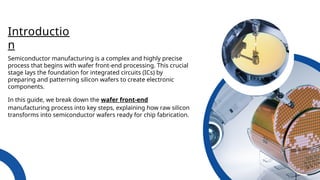
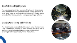
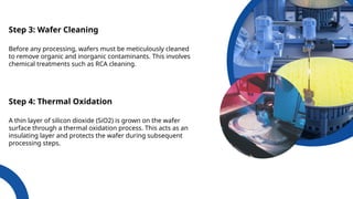


The document presents a step-by-step guide to wafer front-end manufacturing, an essential process for semiconductor production. It details the transformation of raw silicon into wafers through methods like ingot growth, slicing, and polishing, followed by critical processes such as cleaning, thermal oxidation, photolithography, etching, ion implantation, and thin film deposition. This guide emphasizes the importance of each step in creating high-performance integrated circuits and offers insights valuable for engineers, researchers, and technology enthusiasts.


