Sram memory design
•
0 likes•337 views

This SRAM memory architecture minimizes read delay with good stability and small area.

Recommended
More Related Content
What's hot
What's hot (18)
Viewers also liked
Viewers also liked (15)
Similar to Sram memory design
Similar to Sram memory design (20)
Recently uploaded
Recently uploaded (20)
Sram memory design
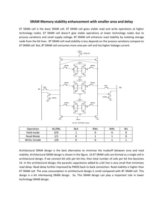
- 1. SRAM Memory stability enhancement with smaller area and delay 6T SRAM cell is the basic SRAM cell. 6T SRAM cell gives stable read and write operations at higher technology nodes. 6T SRAM cell doesn’t give stable operations at lower technology nodes due to process variations and small supply voltage. 8T SRAM cell enhances read stability by isolating storage node from the bit lines. 8T SRAM cell read stability is less depends on the process variations compare to 6T SRAM cell. But, 8T SRAM cell consumes more area per cell and has higher leakage current. Operation BL/RBL BLK RWL WRL WL Hold mode X/X 1 0 0 0 Read Mode 1/1 0 1 1 0 Write 1mode 1/0 0 0 1 1 Architectural SRAM design is the best alternative to minimize the tradeoff between area and read stability. Architectural SRAM design is shown in the figure. 16 6T SRAM cells are formed as a single cell in architectural design. If we connect 64 cells per bit line, then total number of cells per bit line becomes 1K. In this architectural design, the parasitic capacitance added to a bit line is very small that minimizes read delay. Read delay further improved by PMOS back to back connection. Read stability is higher than 6T SRAM cell. The area consumption in architectural design is small compared with 8T SRAM cell. This design is a bit interleaving SRAM design. So, This SRAM design can play a important role in lower technology SRAM design.