Download as PPSX, PPTX


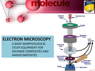
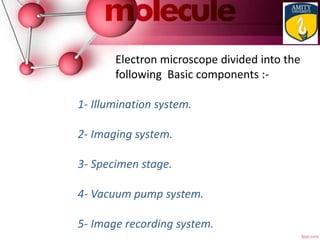

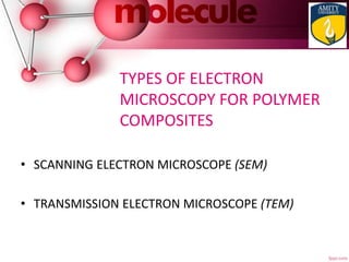
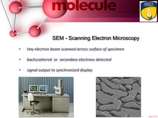
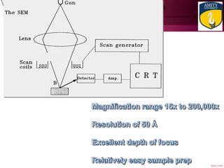
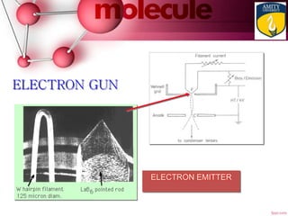
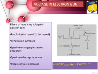


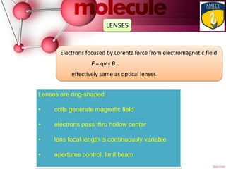
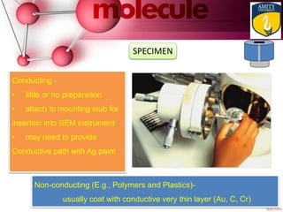
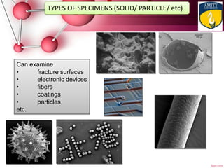

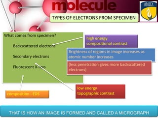

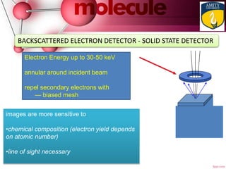
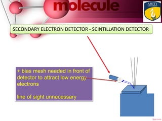
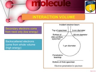
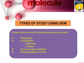


This document provides an overview of scanning electron microscopy (SEM) for analyzing polymer composites and nanocomposites. It describes the basic components of an electron microscope, including the illumination system, imaging system, specimen stage, vacuum pump system, and image recording system. It explains that SEM uses a scanned beam of electrons to produce images of a sample by detecting secondary and backscattered electrons emitted from the surface. The document outlines the signals produced in electron microscopy and discusses scanning electron microscopy and transmission electron microscopy for analyzing polymer composites. It provides details on SEM instrumentation and imaging formation.