Static Ram Design Using Hardware Description Language
1.
External SRAM
A commontype of system RAM is asynchronous static RAM (SRAM).
Access is more complicated than internal memory -- here data, address and control
signals must be asserted in a specific order and held for a specific time.
A memory controller is usually used to shield the synchronous system from SRAM.
It is responsible for generating the properly timed signals and making the
SRAM look ’synchronous’.
Its performance is measured by the number of memory accesses that can be
completed in a given time period.
Designing a memory controller that is optimal is non-trivial.
This set of slides demonstrates the development of a memory controller.
Note that the timing characteristics of an SRAM will differ depending on
the manufacturer, but the same basic principles apply.
1
2.
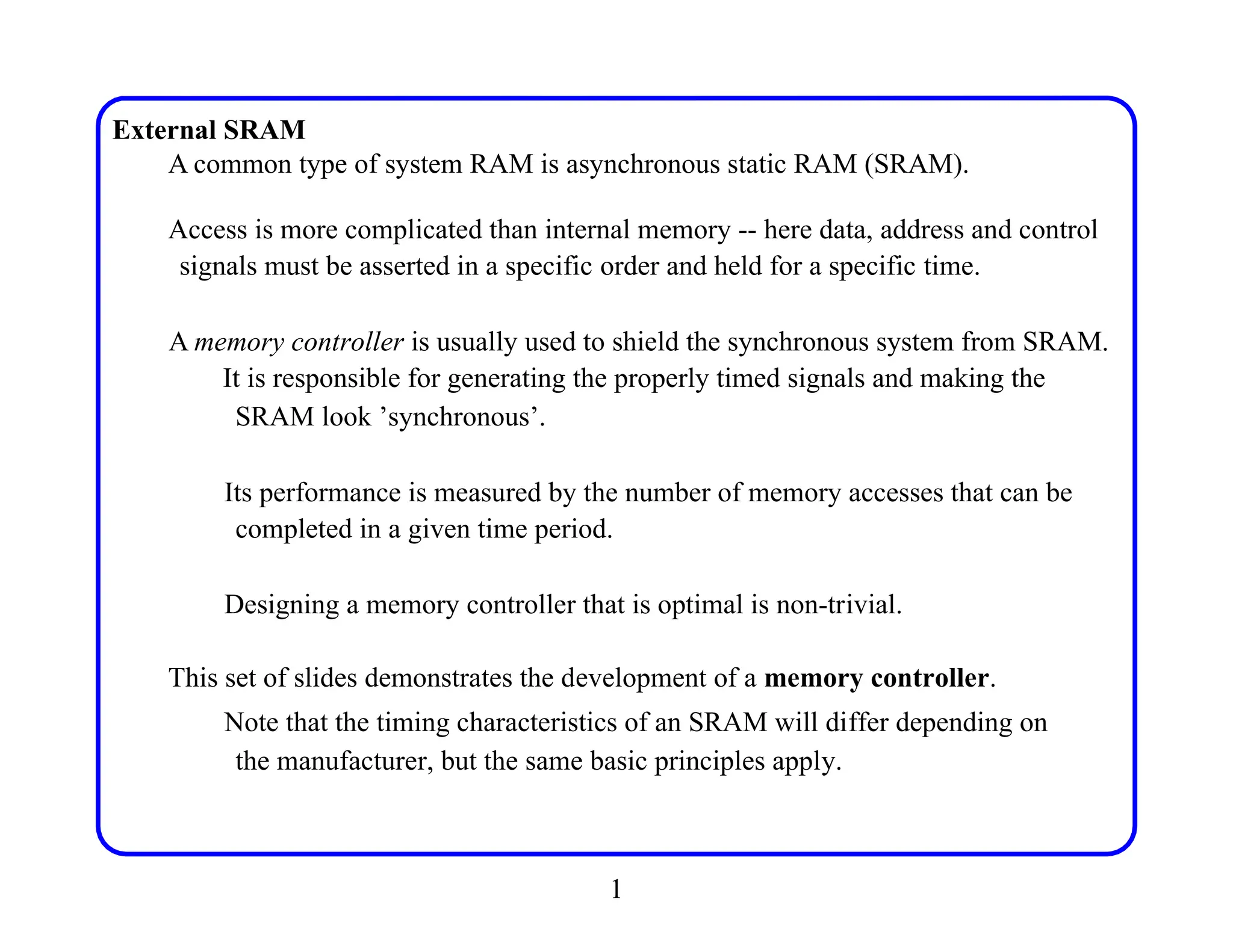
External SRAM
Your boardsdo NOT have external SRAM installed by default but it is available
on
an expansion card.
We have Digilent Memory Modules, C2: 1Mb SRAM, no Flash available.
These expansion cards have two banks of ISSI IS61LV5128AL 512K x 8
SRAM
High-performance, low-power CMOS process with 10 ns access times.
Single 3.3V power supply, static operation: no clock or refresh
required.
Easy memory expansion with CE (power down) and OE options.
Functional
Block Diagram
A0-A18
I/O0-I/O7
I/O
data
circuit
CE
OE
WE
2
Control
circuit
Column I/O
512K X 8
Mem array
Decoder
3.
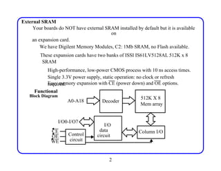
External SRAM
Truth Table:
Thisdevice has a 19-bit address bus (A0-A18), a bi-directional 8-bit data bus (I/O0-
I/
O7) and three active low control signals, CE, OE and WE (see table above).
The timing characteristics of an asynchronouns SRAM are complex and involve
more than 24 parameters -- here we focus on only a few key parameters.
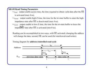
For reading:
• tRC: read cycle time, the min time between two read operations (min 10 ns).
• tAA: address access time, the time required to obtain a stable output data after an
address change (max 10 ns).
• tOHA: output hold time, the time that the output data remains valid after the address
changes (min 2 ns).
3
Mode WE CE OE I/O operation
Not selected (power-down) X H X High-Z
Output disabled H L H High-Z
Read H L L Dout
Write L L X Din
4.
SRAM Read TimingParameters
• tDOE: output enable access time, the time required to obtain valid data after the OE
is activated (max 4 ns).
• tHZOE: output enable high-Z time, the time for the tri-state buffer to enter the high-
impedance state after OE is deactivated (max 4 ns).
• tLZOE: output enable to low-Z time, the time for the tri-state buffer to leave the
high-
impedance state after OE is activated (min 0 ns).
Reading can be accomplished in two ways, with OE activated, changing the address
will change the data; second, OE can be used (for interleaved read/writes).
Timing diagram for address-controlled read cycle
tRC
Address
tAA
tOHA
tOHA
Dout previous data valid data valid
4
5.
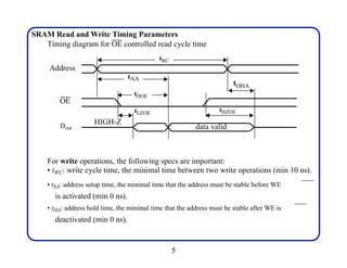
SRAM Read andWrite Timing Parameters
Timing diagram for OE controlled read cycle time
tRC
Address
OHA
OE
Dout
For write operations, the following specs are important:
• tWC: write cycle time, the minimal time between two write operations (min 10 ns).
• tSA: address setup time, the minimal time that the address must be stable before WE
is activated (min 0 ns).
• tHA: address hold time, the minimal time that the address must be stable after WE is
deactivated (min 0 ns).
5
tAA
t
tDOE
tLZOE
tHZOE
HIGH-Z
data valid
6.
SRAM Read andWrite Timing Parameters
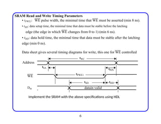
• tPWE1: WE pulse width, the minimal time that WE must be asserted (min 8 ns).
• tSD: data setup time, the minimal time that data must be stable before the latching
edge (the edge in which WE changes from 0 to 1) (min 6 ns).
• tHD: data hold time, the minimal time that data must be stable after the latching
edge (min 0 ns).
Data sheet gives several timing diagrams for write, this one for WE controlled
tWC
Address
tSA
tPWE1
WE
tSD tHD
Din datain valid
6
tHA
Implement the SRAM with the above specifications using HDL
7.
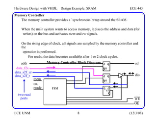
Memory Controller
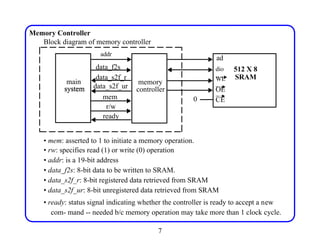
Block diagramof memory controller
data_s2f_ur
system
CE
• mem: asserted to 1 to initiate a memory operation.
• rw: specifies read (1) or write (0) operation
• addr: is a 19-bit address
• data_f2s: 8-bit data to be written to SRAM.
• data_s2f_r: 8-bit registered data retrieved from SRAM
• data_s2f_ur: 8-bit unregistered data retrieved from SRAM
• ready: status signal indicating whether the controller is ready to accept a new
com- mand -- needed b/c memory operation may take more than 1 clock cycle.
7
ad
dio 512 X 8
WE SRAM
OE
main
system
addr
data_f2s
data_s2f_r
memory
controller
mem
r/w
ready
0
8.
Hardware Design withVHDL
Memory Controller
Design Example: SRAM ECE 443
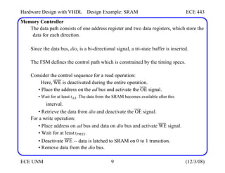
The memory controller provides a ’synchronous’ wrap around the SRAM.
When the main system wants to access memory, it places the address and data (for
writes) on the bus and activates mem and rw signals.
On the rising edge of clock, all signals are sampled by the memory controller and
the
operation is performed.
For reads, the data becomes available after 1 or 2 clock cycles.
Memory Controller Block Diagram
addr
data_f2s
ad
data_s2f_ur
dio
data_s2f_r
en
two read
ports WE
OE
ECE UNM 8 (12/3/08)
d q
en
d q
en
mem
rw
ready FSM q d
9.
Hardware Design withVHDL
Memory Controller
Design Example: SRAM ECE 443
The data path consists of one address register and two data registers, which store the
data for each direction.
Since the data bus, dio, is a bi-directional signal, a tri-state buffer is inserted.
The FSM defines the control path which is constrained by the timing specs.
Consider the control sequence for a read operation:
Here, WE is deactivated during the entire operation.
• Place the address on the ad bus and activate the OE signal.
• Wait for at least tAA. The data from the SRAM becomes available after this
interval.
• Retrieve the data from dio and deactivate the OE signal.
For a write operation:
• Place address on ad bus and data on dio bus and activate WE signal.
• Wait for at least tPWE1.
• Deactivate WE -- data is latched to SRAM on 0 to 1 transition.
• Remove data from the dio bus.
ECE UNM 9 (12/3/08)
10.
Hardware Design withVHDL
Memory Controller
Design Example: SRAM ECE 443
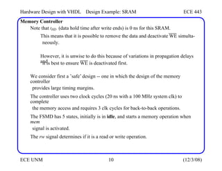
Note that tHD (data hold time after write ends) is 0 ns for this SRAM.
This means that it is possible to remove the data and deactivate WE simulta-
neously.
However, it is unwise to do this because of variations in propagation delays
and
it is best to ensure WE is deactivated first.
We consider first a ’safe’ design -- one in which the design of the memory
controller
provides large timing margins.
The controller uses two clock cycles (20 ns with a 100 MHz system clk) to
complete
the memory access and requires 3 clk cycles for back-to-back operations.
The FSMD has 5 states, initially is in idle, and starts a memory operation when
mem
signal is activated.
The rw signal determines if it is a read or write operation.
ECE UNM 10 (12/3/08)
11.
Hardware Design withVHDL
Memory Controller
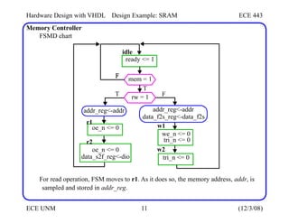
FSMD chart
Design Example: SRAM ECE 443
idle
mem = 1
T
F
rw = 1
addr_reg<-addr
data_f2s_reg<-data_f2s
For read operation, FSM moves to r1. As it does so, the memory address, addr, is
sampled and stored in addr_reg.
ECE UNM 11 (12/3/08)
tri_n <= 0
oe_n <= 0
ready <= 1
addr_reg<-addr
w1
we_n <= 0
w2
tri_n <= 0
F
r1
r2
F
T
oe_n <= 0
data_s2f_reg<-dio
12.
Hardware Design withVHDL
Memory Controller
Design Example: SRAM ECE 443
The oe_n signal is activated in both the r1 and r2 states.
The dio data is sampled and stored in data_s2f_reg on the edge returning the FSM
to
the idle state.
Note that the oe_n signal is deactivated after the state transition is made, and
therefore after the latching event.
Note that the block diagram shown earlier has two read ports.
The data_s2f_r signal is driven by the registers and becomes available
AFTER
the FSM exits the r2 state (and back to idle).
The data on this port remains unchanged until the end of the next read cycle.
The data_s2f_ur signal is connected to the SRAM’s dio bus, with the data
becoming valid at the end of r2 but is REMOVED when the FSM enters
idle.
This port allows the main system (for some apps) to sample/store the data in its
own registers, making it available one cycle earlier (same time as data_s2f_r).
ECE UNM 12 (12/3/08)
13.
Hardware Design withVHDL
Memory Controller
Design Example: SRAM ECE 443
If it had to wait for data_s2f_r to be valid, then the main system would not be able
to
latch the data in its own registers until the NEXT clk cycle.
For the write operation, the FSM moves to the w1 state.
The memory address, addr, and the data, data_f2s, are sampled and stored in
addr_reg and data_f2s_reg registers on the transition to w1.
The we_n and tri_n signals are both activated in state w1.
tri_n enables the tri-state buffer to put the data on the SRAM’s dio
bus.
On the transition to w2, we_n is deactivated but tri_n remains activated.
This ensures the data is properly latched to the SRAM when we_n changes
from
0 to 1.
At the end of the write cycle, the FSM returns to idle and tri_n is deactivated to
remove the data from the dio bus.
ECE UNM 13 (12/3/08)
14.
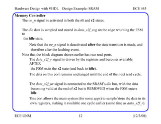
Hardware Design withVHDL Design Example: SRAM ECE 443
Timing Analysis of Memory Controller
We must verify the memory controller meets the timing specs. for the SRAM
chip.
With a 100 MHz system clock, the FSM stays in each state for 10 ns.
For a read cycle, oe_n is asserted for two states, totaling 20 ns.
This provides a 10 ns margin over the 10 ns tAA.
Deactivating oe_n in r1 imposes a more stringent timing constraint.
The data is stored in the data_s2f_reg when the FSM moves to idle.
Although oe_n is deactivated at the transition, the data remains valid for a
small
interval b/c the FPGA’s pad delay and
the
tHZOE delay (4 ns) of the SRAM.
During the write cycle, we_n is asserted in w1 -- the 10 ns interval exceeds
the
spec (min 8 ns).
tPWE1
tri_n remains activated in w2 and thus ensures the data is still stable during the 0 ->
1
transition of the we_n signal.
ECE UNM 14 (12/3/08)
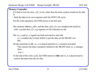
15.
Hardware Design withVHDL Design Example: SRAM ECE 443
Timing Analysis of Memory Controller
In terms of performance, both read and write operations take two clock cycles
to
complete.
During the read operation, the unregistered data (data_s2f_ur) is available at the end
of the second cycle (right before the rising edge)
While the registered data is available after the clock edge.
Note that both operations require a return to idle and therefore the sustained rate is 3
clocks (not 2).
With regard to the HDL implementation, the memory controller must generate fast,
glitch-free control signals.
The output logic can be modified to include Moore look-ahead output buffers.
This scheme adds a buffer (DFF) for each output signal to remove glitches
and reduce clock-to-output delay.
ECE UNM 15 (12/3/08)
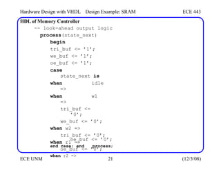
16.
Hardware Design withVHDL
HDL of Memory Controller
Design Example: SRAM ECE 443
To compensate for the added clock cycle, we ’look ahead’ at the state’s future
value
(state_next signal) and use it to replace the state_reg signals in the output logic.
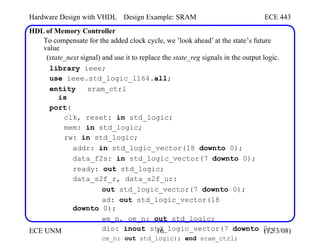
library ieee;
use ieee.std_logic_1164.all;
entity sram_ctrl
is
port(
clk, reset: in std_logic;
mem: in std_logic;
rw: in std_logic;
addr: in std_logic_vector(18 downto 0);
data_f2s: in std_logic_vector(7 downto 0);
ready: out std_logic;
data_s2f_r, data_s2f_ur:
out std_logic_vector(7 downto 0);
ad: out std_logic_vector(18
downto 0);
we_n, oe_n: out std_logic;
dio: inout std_logic_vector(7 downto 0);
ce_n: out std_logic); end sram_ctrl;
ECE UNM 16 (12/3/08)
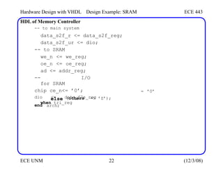
17.
Hardware Design withVHDL
HDL of Memory Controller
Design Example: SRAM ECE 443
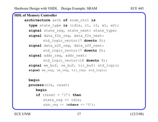
architecture arch of sram_ctrl is
type state_type is (idle, r1, r2, w1, w2);
signal state_reg, state_next: state_type;
signal data_f2s_reg, data_f2s_next:
std_logic_vector(7 downto 0);
signal data_s2f_reg, data_s2f_next:
std_logic_vector(7 downto 0);
signal addr_reg, addr_next:
std_logic_vector(18 downto 0);
signal we_buf, oe_buf, tri_buf: std_logic;
signal we_reg, oe_reg, tri_reg: std_logic;
begin
process(clk, reset)
begin
if (reset = ’1’) then
state_reg <= idle;
addr_reg <= (others => ’0’);
ECE UNM 17 (12/3/08)
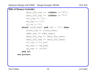
Hardware Design withVHDL
HDL of Memory Controller
Design Example: SRAM ECE 443
-- next state logic
process(state_reg, mem, rw, dio, addr, data_f2s,
data_f2s_reg, data_s2f_reg, addr_reg)
begin
addr_next <= addr_reg;
data_f2s_next <= data_f2s_reg;
data_s2f_next <= data_s2f_reg;
ready <= ’0’;
case
state_reg is
when
idle =>
if (mem = ’0’) then
state_next <= idle;
else
addr_next <= addr;
if (rw = ’0’) then -- write
state_next <=
data_f2s_next
else
w1;
<= data_f2s;
ECE UNM 19 (12/3/08)
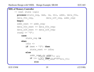
20.
Hardware Design withVHDL
HDL of Memory Controller
Design Example: SRAM ECE 443
state_next <=
end if;
end if;
ready <= ’1’;
when w1 =>
r1;
state_next
when w2 =>
state_next
when r1 =>
state_next
when r2 =>
<= w2;
<= idle;
<= r2;
data_s2f_next
state_next <=
end case;
end process;
<= dio;
idle;
ECE UNM 20 (12/3/08)
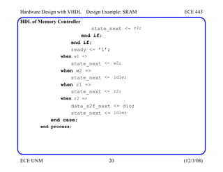
21.
Hardware Design withVHDL
HDL of Memory Controller
Design Example: SRAM ECE 443
-- look-ahead output logic
process(state_next)
begin
tri_buf <= ’1’;
we_buf <= ’1’;
oe_buf <= ’1’;
case
state_next is
when idle
=>
when w1
=>
tri_buf <=
’0’;
we_buf <= ’0’;
when w2 =>
tri_buf <= ’0’;
when r1 =>
oe_buf <= ’0’;
when r2 =>
oe_buf
end case; end
<= ’0’;
process;
ECE UNM 21 (12/3/08)
22.
Hardware Design withVHDL
HDL of Memory Controller
-- to main system
Design Example: SRAM ECE 443
data_s2f_r <= data_s2f_reg;
data_s2f_ur <= dio;
-- to SRAM
we_n <= we_reg;
oe_n <= oe_reg;
ad <= addr_reg;
-- I/O
for SRAM
chip ce_n<= ’0’;
dio <= data_f2s_reg
when tri_reg
= ’0’
else
arch;
(others => ’Z’);
end
ECE UNM 22 (12/3/08)
23.
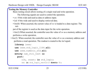
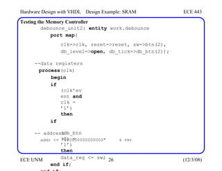
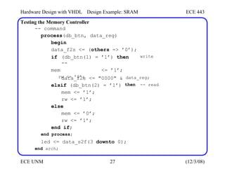
Hardware Design withVHDL Design Example: SRAM ECE 443
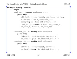
Testing the Memory Controller
Basic testing circuit allows testing of a single read and write operation.
The following signals are used to control the operation.
• sw: 4 bits wide and used as data or address input.
• led: 4 bits wide and used to display retrieved data.
• btn(0): When asserted, the current value of sw is loaded to a data register. The
out-
put of the register is used as the data input for the write operation.
• btn(1):When asserted, the controller uses the value of sw as a memory address and
performs a write operation.
• btn(2): When asserted, the controller uses the value of sw as a memory address and
performs a read operation. The readout is routed to the led signal.
library ieee;
use ieee.std_logic_1164.all;
use ieee.numeric_std.all;
entity ram_ctrl_test is
port(
clk, reset: in std_logic;
sw: in std_logic_vector(3 downto 0);
ECE UNM 23 (12/3/08)
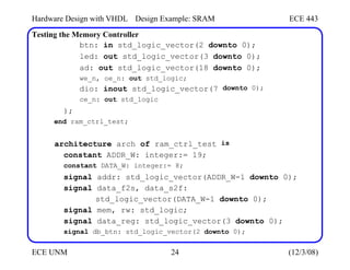
24.
Hardware Design withVHDL Design Example: SRAM ECE 443
Testing the Memory Controller
btn: in std_logic_vector(2 downto 0);
led: out std_logic_vector(3 downto 0);
ad: out std_logic_vector(18 downto 0);
we_n, oe_n: out std_logic;
dio: inout std_logic_vector(7
ce_n: out std_logic
downto 0);
);
end ram_ctrl_test;
architecture arch of ram_ctrl_test
constant ADDR_W: integer:= 19;
constant DATA_W: integer:= 8;
is
signal addr: std_logic_vector(ADDR_W-1 downto 0);
signal data_f2s, data_s2f:
std_logic_vector(DATA_W-1 downto 0);
signal mem, rw: std_logic;
signal data_reg: std_logic_vector(3 downto 0);
signal db_btn: std_logic_vector(2 downto 0);
ECE UNM 24 (12/3/08)