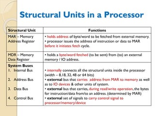
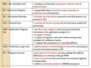
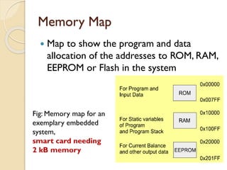
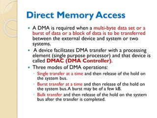
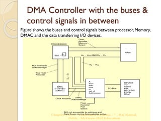
SlideShare a Scribd company logo
Unit 2
PROCESSOR AND
MEMORY ORGANIZATION
By,
Mrs. Pavithra S
Asst. Prof.
GSSSIETW, Mysuru
Karnataka
Contents
1. Structural Units in a Processor
2. Processor selection for an Embedded System
3. Memory Devices
4. Memory Selection for an Embedded System
5. Allocation of memory to Program segments &
Blocks and Memory map of a system
6. Direct Memory Access
7. Interfacing Processor
8. Memories and Input Output Devices
Structural Units in a Processor
Structural Unit Functions
MAR – Memory
Address Register
• holds address of byte/word to be fetched from external memory.
• processor issues the address of instruction or data to MAR
before it initiates fetch cycle.
MDR – Memory
Data Register
• holds a byte/word fetched (to be sent) from (to) an external
memory / IO address.
System Buses
1. Internal Bus
2. Address Bus
3. Data Bus
4. Control Bus
• internally connects all the structural units inside the processor
(width – 8,18, 32, 48 or 64 bits)
• external bus that carries address from MAR to memory as well
as to IO devices & other units of system.
• external bus that carries, during read/write operation, the bytes
for instruction/data from/to an address. (determined by MAR)
• external set of signals to carry control signal to
processor/memory/device
BIU – Bus Interface Unit • interface unit between processor’s internal units &
external buses
IR – Instruction Register • sequentially takes instruction codes (opcode) to
execution unit of processor.
ID – Instruction Decoder • decodes the instruction received at the IR & passes it to
processor CU.
CU – Control Unit • controls all the bus activities & unit functions needed for
processing.
ARS – Application Register
Set
• set of on-chip registers used during processing of
instruction of an application program or
• a register window
• a subset of registers with each subset storing static
variables of a software routine
• a register file associated to a unit (ALU/FPLU)
ALU – Arithmetic Logic Unit • unit to execute arithmetic/logical instruction according to
current instruction present at IR.
PC – Program Counter • generates an instruction cycle by sending the address
defined by it to memory through MAR
• auto increments as the instructions are fetched regularly
& sequentially
• called as instruction pointer in 80x86 processors
SP – Stack Pointer • pointer for an address which corresponds to a stack top in
memory.
IQ – Instruction
Queue
• queue of instructions so that IR does nit have to wait for next
instruction
PFCU – Pre-fetch
Control Unit
• unit that controls the fetching of data into I- & D- caches in
advance from memory units.
• improve performance by fetching instructions and data in
advance for processing.
I- Cache – Instruction
Cache
• sequentially stores (like instruction queue) instructions in FIFO
mode.
• lets the processor execute instructions at greater speed using
PFCU.
D- Cache –
Data Cache
• stores pre-fetch data from external memory.
• stores both key and value together at a location.
• also stores write-through data when configured.
BT- Cache – Branch
Target Cache
• facilitate ready availability of the next instruction-set when a
branch instruction like JUMP/LOOP/CALL is encountered.
MMU – Memory
Management Unit
• manages the memories such that the instructions and date are
readily available for processing.
SRS – System
Register Set
• set of registers used while processing the instructions of the
supervisory system program.
FLPU – Floating Point
Processing Set
• separate unit from ALU for floating point processing
which is essential in processing mathematical function
fast in a microprocessor/DSP
FRS – Floating point Register
Set
• register set dedicated for storing floating point
numbers in a standard format and used by FLPU for its
data & stack.
MAC – Multiply and
Accumulate unit
• units for multiplying coefficients of a series and
accumulating these during computations.
AOU – Atomic Operation
Unit
• it lets a user/compiler instructions when broken into
a number of processor instructions called atomic
operations, finish before an interrupt of a process
occurs.
• it prevents problems from arising out of shared data
between various routines and tasks.
Organisation of various structural units of processor
Units shown with dashed boundary are present in the high performance processors only
Features in most processors
1. Instruction CycleTime:
◦ It’s the time taken by a processor to execute a simple instruction ( ˜1µs
for 8051- ˜1.6ns for MPC604 )
◦ System designer uses as an indicator to match the processor speed with
application
2. Internal BusWidth:
◦ ALU gets inputs through internal buses
◦ 32 bit bus to facilitate the availability of arithmetic operations on 32-bit
operands in a single cycle
◦ 32-bit bus – a necessity for signal processing and control system instructions
3. Program-Counter (PC) bits & Reset value:
◦ Number of PC bits decides maximum possible size of physical memory that
can be accessed by the processor
◦ Reset value tells the designer the initial program address from where the
program runs on a system reset/power up
4. Stack-Pointer bits & initial reset value
◦ SP values must point to addresses of the words stored at
stack
◦ Software designer defines an initial reset value & sets the
beginning SP accordingly
5. Interrupt Controller
◦ To program the service routine priorities and to allocate
vector addresses
6. Direct Memory Access (DMA) controller with
multiple channels
◦ More number of I/O devices needs to access a multi byte data
set faster, DMA is useful.
Features in most processors
PROCESSOR SELECTION
Processor specific feature:
1. Should operate at higher clock speed for processing more
instructions per second.
2. High computing performance when there exist
◦ (a) Pipeline(s) and superscalar architectures,
◦ (b) pre-fetch cache unit, caches, and register-files and MMU and
(c) RISC architecture.
3. Register-windows provides fast context switching in a
multitasking system.
4. Power-efficient embedded system requires a processor
that has auto-shut down feature for its units and
programmability for the disabling use of caches when the
processing need for a function or instruction set is not
constrained by limit or execution time. Uses Stop, Sleep
and Wait instructions, also require special cache design.
Processor specific feature:
5. Burst mode accesses external memories fast, reads
fast and writes fast.
6. Atomic operation unit provides hardware solution to
shared data problem when designing embedded
software, else special programming skill and efforts
are to be made when sharing the variables among the
multiple tasks.
7. Big-endian (MSB to lowest address) or Little-endian
(LSB to lowest address)
8. Energy efficient
Case Studies:
 Case-1
◦ Systems in which processor instruction cycle time
is ˜1µs and on-chip devices & memory can suffice.
◦ Examples:Automatic chocolate vending machine,
robots, data acquisition systems
 Case-2
◦ Systems in which processor instruction cycle
time is ˜10 to 40ns and on-chip devices &
memory do not suffice and medium processor
performance required.
◦ Examples: 2Mbps router, image processing, voice data
acquisition, voice compression
Case Studies:
 Case-3
◦ Systems in which instruction cycle time is 5 to 10ns
required and high MIPS/MFLOPS performance needed.
◦ Examples: Multiport 100Mbps network transceiver, fast
100Mbps switches, router
 Case-4
◦ Systems in which instruction cycle time of even1ns
does not suffice and multi-processor system is required
along with use of floating point & MAC unit.
◦ Examples:Voice processing,Video processing, Real-time
audio/video processing
MEMORY DEVICES
 A simple credit-debit transaction card may
require just 2kB of memory.
◦ On other hand, smart card for secure transactions
(cryptographic functions) require 32kB of memory.
 A memory- a data byte, or a word, or a double
word, or a quad word may be accessed from
all addressable locations with a similar process
and there is would be equal access time for
a read or for a write operation.
ROM : Uses, Forms &Variants
 Non-Volatility is an important asset useful to
embed codes & data in a system.
 ROM embeds software/application logic circuit in
either forms – Masked ROM, PROM &
EPROM.
 During runtime programming EEPROM/Flash
memory is used.
Masked ROM
 One time masking charge – very high
 Therefore, system manufacturer will
place order & manufacturing foundry will
accept the order for a minimum of 1000
pieces.
 ROM is a cost effective solution to a bulk
user.
EPROM, EEPROM and OTP ROM
 EPROM:
◦ It is an ultraviolet ray erasable & device
programmable.
◦ Erasing means restoring 1 at each bit.
 EEPROM:
◦ Electrically Erasable and Programmable Read Only
Memory
 Flash Memory:
◦ Form of EEPROM, in which sector of bytes can be
erased in a flash.
 PROM:
◦ Once written is not erasable.
◦ OTP (One Time device Programmer)
RAM – Random Access Memory
 A system designer considers RAM devices of EIGHT
forms.
1. SRAM – Static RAM,
2. DRAM – Dynamic RAM,
3. NVRAM – NonVolatile RAM,
4. EDORAM – Extended Data Output RAM,
5. SDRAM – Synchronous DRAM,
6. RDRAM – Rambus DRAM,
7. Parameterized distributed RAM and
8. Parameterized Block RAM.
USES:
 Stores variables during a program run & stores stack.
 Stores input & output buffers.
◦ Eg: Speech & Image
1. SRAM: commonly used for designing caches &
in embedded systems and microcontrollers.
2. DRAM: mostly used in high performance
computers / high memory density systems.
3. EDORAM: used for system having buses with
clock rates up to 100MHz.
4. SDRAM: synchronizes read operations &
keeps next word ready, used for processor
speed of 1GHz.
5. RDRAM: accesses in burst (four successive
words in a single fetch), thus performance
1GHz speed.
6. Parameterized distributed RAM:
distributes in various system sub-units -
IO buffers & transceiver sub-units.
Distribution buffering of memory &
facilitates faster inputs from IO devices.
7. Parameterized Block RAM: used when
specific block of RAM is dedicated to sub-
unit (eg: MAC unit), used when access by
the system / IO / Internal bus is slow
compared to processing speed of sub-unit.
Summary of Memory
 Masked ROM/EPROM/Flash stores embedded software
(ROM image). Masked ROM is for bulk manufacturing.
 EPROM / EEPROM is used for testing & design stages.
 EEPROM is used to store the results during program
runtime (erased byte-by-byte and written during
system run).
 Flash is useful when a processed image /voice /data
/system configuration has to be stored.
 RAM is mostly used in SRAM form
Memory Selection for an
Embedded System
 Once Software designer’s coding is over and the
ROM image file is ready, a hardware designer is faced
with the questions, of what type of memory and what
size of each should be used.
 CASE STUDIES:
1. Automatic chocolate vending machine or real time
robotic control system.
2. Data Acquisition Systems
3. Multi-pot network transceivers, Fast switches, Routers,
or Multi-channel Fast Encryption and decryption System
4. Voice processor or video processing or Mobile Phone
system
5. Digital Camera orVideo recorder system.
Allocation of MemoryTo
Program Segments and Blocks
 Functions, Processes, Data and Stacks at theVarious
Segments of Memory:
◦ Program routines & processes can have different
segments.
◦ A pointer address, points to the start of memory block
storing a segment and an offset value is used to retrieve
for a memory address within that segment.
 Segment wise memory allocation in four segments:
Code, Data, Stack and Extra
(for examples, image, String)
Segments and Paging at the Memory
 A segment can have partitions of fixed
sizes called PAGES.
◦ Figure shows different segment types required
by software designer.
Each Segment has a starting and
ending memory address.
Each Segment has a pointer and
an offset address.
Using offset, code / data is
retrieved from a segment
Different Data Structures/Sets at
Various Memory Blocks
1) Stacks –
• allotted memory
block, from which
data is read (LIFO)
• Return addresses on
the nested calls,
• Sets of LIFO (Last In
First Out)
retrievable data,
• Saved Contexts of
the tasks as the
stacks
2) Arrays – One dimensional or multidimensional
data can be retrieved from any element
address.
3) Queues – Sets of FIFO (First In First Out)
retrievable data;Two pointer (Front/Head & Back/Tail)
Circular Queue (Example- a Printer Buffer);
bounded memory block, on exceeding limit reset to start.
PIPE / Block Queue (Example- a network stack)
common memory block allotted for a queue with source &
destination.
For Circular Queue, when back attempts
To exceed end, back becomes equal to start.
4) Table – two dimensional array (matrix)
three pointers – table base, column index, destination index pointer
5) HashTable – collection of pairs of key &
corresponding value.
data set allocated with a memory block - Look-up-table
6) List – a data structure with number of memory
blocks, one for each element.
each list-element stores pointer to next element
last element points to NULL
A list is for non-consecutively located objects
at the memory.
The Memory Maps
Fig (a) - Princeton
and
Fig (b) - Harvard
Memory
Organizations
The Memory Maps
 Memory areas needed in the case of Princeton
and Harvard architecture are different and as
shown
◦ Vectors and pointers, variables, program segments
and memory blocks for data and stacks have different
addresses in the program – PRINCETON memory
architecture.
◦ Program segments and memory blocks for data and
stacks have separate sets of addresses in Harvard
architecture. Control signals and read-write
instructions are also separate.
 Designer must remember that if main memory is
of Harvard architecture, program memory map
will be separate.
Memory Map
 Map to show the program and data
allocation of the addresses to ROM, RAM,
EEPROM or Flash in the system
Fig: Memory map for an
exemplary embedded
system,
smart card needing
2 kB memory
Direct Memory Access
 A DMA is required when a multi-byte data set or a
burst of data or a block of data is to be transferred
between the external device and system or two
systems.
 A device facilitates DMA transfer with a processing
element (single purpose processor) and that device is
called DMAC (DMA Controller).
 Three modes of DMA operations:
◦ Single transfer at a time and then release of the hold on
the system bus.
◦ Burst transfer at a time and then release of the hold on
the system bus.A burst may be of a few kB.
◦ Bulk transfer and then release of the hold on the system
bus after the transfer is completed.
DMAC - DMA Controller
 Data transfer occurs efficiently between I/O
devices and system memory with the least
processor intervention using DMAC.
 DMAC provide memory access to Multiple
channels
◦ Separate set of registers for programming each
channel.
◦ Separate interrupt signals in the case of a multi-
channel DMAC
 Provides DMA action from system memories
and two (or more IO) devices.
DMA Controller with the buses &
control signals in between
Figure shows the buses and control signals between processor, Memory,
DMAC and the data transferring I/O devices.
DMA Controller Execution
 DMA proceeds without the CPU intervening
◦ Except
(i) at the start for DMAC programming and
initializing and
(ii) at the end.
◦ Whenever a DMA request by external device is
made to the DMAC, the CPU is requested (using
interrupt signal) the DMA transfer by DMAC at
the start to initiate the DMA and at the end to
notify (using interrupt signal) the end of the
DMA by DMAC.
Interfacing Processor, Memories
& Input Output Devices
 Interconnections for a simple bus structure has three sets
of signals – data, address and control signals.
 A system-bus interfacing-design is according to the timing
diagrams of processor signals, speed and word length for
instructions and data.
 Interfacing of processor, memory and IO devices using
memory system bus
Time division multiplexed (TDM)
address and data bits for the memories
 TDM ─ Different time slots, there is a different sets
(channel) of the signals.
 Address signals during one time slot and
data bus signals in another time slot.
 Interfacing circuit for the demultiplexing of the buses
uses a control signal.
 Control signal - Address Latch Enable (ALE) in 8051,
Address Strobe (AS) in 68HC11 and address valid
(ADV) in 80196.
 ALE or AS or ADV demultiplexes the address and data
buses to the devices
Interfacing circuit using Latch and
decoders
 ALE for latching the address
 PSEN (Program Store ENable) for program
memory read using address data buses
 Each chip of the memory or port that
connects the processor has a separate chip
select input from a decoder.
 Decoder is a circuit, which has appropriate
signals of the address bus at the input and
control circuit signals to generate
corresponding CS (chip select) control
signals for each device (memory and ports)
Summary: Interfacing- circuit
 Consists of latches, decoders and demultiplexers
 Designed as per available control signals and
timing diagrams of the bus signals.
 Circuit connects all the units, processor, memory
and the IO device through the system buses.
 Also called glue circuit used as it joins the
devices and memory with the system bus and
processor
 Can be designed using a GAL (generic array
logic) or FPGA
Memory system bus and I/O bus
interconnections in a bus structure

More Related Content

What's hot

Ch 1 introduction to Embedded Systems (AY:2018-2019--> First Semester)
Ch 1 introduction to Embedded Systems (AY:2018-2019--> First Semester)Ch 1 introduction to Embedded Systems (AY:2018-2019--> First Semester)
Ch 1 introduction to Embedded Systems (AY:2018-2019--> First Semester)
Moe Moe Myint
 
Quality attributes of Embedded Systems
Quality attributes of Embedded Systems Quality attributes of Embedded Systems
Quality attributes of Embedded Systems
VijayKumar5738
 
Automatic chocolate vending machine using mucos rtos ppt
Automatic chocolate vending machine using mucos rtos pptAutomatic chocolate vending machine using mucos rtos ppt
Automatic chocolate vending machine using mucos rtos ppt
JOLLUSUDARSHANREDDY
 
Addressing modes of 8051
Addressing modes of 8051Addressing modes of 8051
Addressing modes of 8051
SARITHA REDDY
 
Issues in routing protocol
Issues in routing protocolIssues in routing protocol
Issues in routing protocol
Pradeep Kumar TS
 
Real Time Kernels
Real Time KernelsReal Time Kernels
Real Time KernelsArnav Soni
 
Serial Communication in 8051
Serial Communication in 8051Serial Communication in 8051
Serial Communication in 8051
Sudhanshu Janwadkar
 
Fault tolerance techniques for real time operating system
Fault tolerance techniques for real time operating systemFault tolerance techniques for real time operating system
Fault tolerance techniques for real time operating system
anujos25
 
cellular concepts in wireless communication
cellular concepts in wireless communicationcellular concepts in wireless communication
cellular concepts in wireless communicationasadkhan1327
 
Serial Communication Interfaces
Serial Communication InterfacesSerial Communication Interfaces
Serial Communication Interfaces
anishgoel
 
Handoff in Mobile Communication
Handoff in Mobile CommunicationHandoff in Mobile Communication
Handoff in Mobile Communication
Noushad Hasan
 
CELLULAR MOBILE RADIO SYSTEMS
CELLULAR MOBILE RADIO SYSTEMSCELLULAR MOBILE RADIO SYSTEMS
CELLULAR MOBILE RADIO SYSTEMS
VenkataSatya Manchikalapati
 
Unit II Arm7 Thumb Instruction
Unit II Arm7 Thumb InstructionUnit II Arm7 Thumb Instruction
Unit II Arm7 Thumb Instruction
Dr. Pankaj Zope
 
WSN network architecture -Sensor Network Scenarios & Transceiver Design Consi...
WSN network architecture -Sensor Network Scenarios & Transceiver Design Consi...WSN network architecture -Sensor Network Scenarios & Transceiver Design Consi...
WSN network architecture -Sensor Network Scenarios & Transceiver Design Consi...
ArunChokkalingam
 
Direct memory access (dma)
Direct memory access (dma)Direct memory access (dma)
Direct memory access (dma)
Zubair Khalid
 
IS-95 Cdma
IS-95 CdmaIS-95 Cdma
IS-95 Cdma
yogesh singh
 
Introduction to Embedded Architecture
Introduction to Embedded Architecture Introduction to Embedded Architecture
Introduction to Embedded Architecture
amrutachintawar239
 
Sonet (synchronous optical networking )
Sonet (synchronous optical networking )Sonet (synchronous optical networking )
Sonet (synchronous optical networking )
Hamza Sajjad
 
Unit 1 Introduction to Embedded computing and ARM processor
Unit 1 Introduction to Embedded computing and ARM processorUnit 1 Introduction to Embedded computing and ARM processor
Unit 1 Introduction to Embedded computing and ARM processor
Venkat Ramanan C
 

What's hot (20)

Ch 1 introduction to Embedded Systems (AY:2018-2019--> First Semester)
Ch 1 introduction to Embedded Systems (AY:2018-2019--> First Semester)Ch 1 introduction to Embedded Systems (AY:2018-2019--> First Semester)
Ch 1 introduction to Embedded Systems (AY:2018-2019--> First Semester)
 
Quality attributes of Embedded Systems
Quality attributes of Embedded Systems Quality attributes of Embedded Systems
Quality attributes of Embedded Systems
 
Automatic chocolate vending machine using mucos rtos ppt
Automatic chocolate vending machine using mucos rtos pptAutomatic chocolate vending machine using mucos rtos ppt
Automatic chocolate vending machine using mucos rtos ppt
 
Addressing modes of 8051
Addressing modes of 8051Addressing modes of 8051
Addressing modes of 8051
 
Issues in routing protocol
Issues in routing protocolIssues in routing protocol
Issues in routing protocol
 
Real Time Kernels
Real Time KernelsReal Time Kernels
Real Time Kernels
 
Serial Communication in 8051
Serial Communication in 8051Serial Communication in 8051
Serial Communication in 8051
 
Fault tolerance techniques for real time operating system
Fault tolerance techniques for real time operating systemFault tolerance techniques for real time operating system
Fault tolerance techniques for real time operating system
 
cellular concepts in wireless communication
cellular concepts in wireless communicationcellular concepts in wireless communication
cellular concepts in wireless communication
 
Serial Communication Interfaces
Serial Communication InterfacesSerial Communication Interfaces
Serial Communication Interfaces
 
Handoff in Mobile Communication
Handoff in Mobile CommunicationHandoff in Mobile Communication
Handoff in Mobile Communication
 
CELLULAR MOBILE RADIO SYSTEMS
CELLULAR MOBILE RADIO SYSTEMSCELLULAR MOBILE RADIO SYSTEMS
CELLULAR MOBILE RADIO SYSTEMS
 
Unit II Arm7 Thumb Instruction
Unit II Arm7 Thumb InstructionUnit II Arm7 Thumb Instruction
Unit II Arm7 Thumb Instruction
 
Power control in 3 g
Power control in 3 gPower control in 3 g
Power control in 3 g
 
WSN network architecture -Sensor Network Scenarios & Transceiver Design Consi...
WSN network architecture -Sensor Network Scenarios & Transceiver Design Consi...WSN network architecture -Sensor Network Scenarios & Transceiver Design Consi...
WSN network architecture -Sensor Network Scenarios & Transceiver Design Consi...
 
Direct memory access (dma)
Direct memory access (dma)Direct memory access (dma)
Direct memory access (dma)
 
IS-95 Cdma
IS-95 CdmaIS-95 Cdma
IS-95 Cdma
 
Introduction to Embedded Architecture
Introduction to Embedded Architecture Introduction to Embedded Architecture
Introduction to Embedded Architecture
 
Sonet (synchronous optical networking )
Sonet (synchronous optical networking )Sonet (synchronous optical networking )
Sonet (synchronous optical networking )
 
Unit 1 Introduction to Embedded computing and ARM processor
Unit 1 Introduction to Embedded computing and ARM processorUnit 1 Introduction to Embedded computing and ARM processor
Unit 1 Introduction to Embedded computing and ARM processor
 

Similar to Unit 2 processor&memory-organisation

Introduction to embedded systems
Introduction  to embedded systemsIntroduction  to embedded systems
Introduction to embedded systems
RAMPRAKASHT1
 
Computer Organization: Introduction to Microprocessor and Microcontroller
Computer Organization: Introduction to Microprocessor and MicrocontrollerComputer Organization: Introduction to Microprocessor and Microcontroller
Computer Organization: Introduction to Microprocessor and Microcontroller
AmrutaMehata
 
Chap 3 CA.pptx
Chap 3 CA.pptxChap 3 CA.pptx
Chap 3 CA.pptx
SahalAhmed4
 
BAIT1003 Chapter 2
BAIT1003 Chapter 2BAIT1003 Chapter 2
BAIT1003 Chapter 2
limsh
 
Introduction to embedded System.pptx
Introduction to embedded System.pptxIntroduction to embedded System.pptx
Introduction to embedded System.pptx
Pratik Gohel
 
Topic 5 Digital Technique basic computer structure
Topic 5 Digital Technique basic computer structureTopic 5 Digital Technique basic computer structure
Topic 5 Digital Technique basic computer structure
Bai Haqi
 
I. Introduction to Microprocessor System.ppt
I. Introduction to Microprocessor System.pptI. Introduction to Microprocessor System.ppt
I. Introduction to Microprocessor System.ppt
HAriesOa1
 
Co notes3 sem
Co notes3 semCo notes3 sem
Co notes3 sem
dilshad begum
 
Cpu
CpuCpu
11. Computer Systems Hardware 1
11. Computer Systems   Hardware 111. Computer Systems   Hardware 1
11. Computer Systems Hardware 1New Era University
 
Chapter01 (1).ppt
Chapter01 (1).pptChapter01 (1).ppt
Chapter01 (1).ppt
AvadhRakholiya3
 
esunit1.pptx
esunit1.pptxesunit1.pptx
esunit1.pptx
AmitKumar7572
 
Computer Organisation & Architecture (chapter 1)
Computer Organisation & Architecture (chapter 1) Computer Organisation & Architecture (chapter 1)
Computer Organisation & Architecture (chapter 1)
Subhasis Dash
 
Embedded systems 101 final
Embedded systems 101 finalEmbedded systems 101 final
Embedded systems 101 final
Khalid Elmeadawy
 
Challenges in Embedded Computing
Challenges in Embedded ComputingChallenges in Embedded Computing
Challenges in Embedded Computing
Pradeep Kumar TS
 
1.CPU INSTRUCTION AND EXECUTION CYCLEThe primary function of the .pdf
1.CPU INSTRUCTION AND EXECUTION CYCLEThe primary function of the .pdf1.CPU INSTRUCTION AND EXECUTION CYCLEThe primary function of the .pdf
1.CPU INSTRUCTION AND EXECUTION CYCLEThe primary function of the .pdf
aniyathikitchen
 
ch1.pptx
ch1.pptxch1.pptx
ch1.pptx
berekethailu2
 
HHCJ AMUMARA:COMPUTER STUDIES LECTURE NOTE FOR SS3:005
HHCJ AMUMARA:COMPUTER STUDIES LECTURE NOTE FOR SS3:005HHCJ AMUMARA:COMPUTER STUDIES LECTURE NOTE FOR SS3:005
HHCJ AMUMARA:COMPUTER STUDIES LECTURE NOTE FOR SS3:005
SOLOMONCHINAEMEUCHEA
 
CAO.pptx
CAO.pptxCAO.pptx
CAO.pptx
FarhanaMariyam1
 

Similar to Unit 2 processor&memory-organisation (20)

Introduction to embedded systems
Introduction  to embedded systemsIntroduction  to embedded systems
Introduction to embedded systems
 
Computer Organization: Introduction to Microprocessor and Microcontroller
Computer Organization: Introduction to Microprocessor and MicrocontrollerComputer Organization: Introduction to Microprocessor and Microcontroller
Computer Organization: Introduction to Microprocessor and Microcontroller
 
Chap 3 CA.pptx
Chap 3 CA.pptxChap 3 CA.pptx
Chap 3 CA.pptx
 
BAIT1003 Chapter 2
BAIT1003 Chapter 2BAIT1003 Chapter 2
BAIT1003 Chapter 2
 
Introduction to embedded System.pptx
Introduction to embedded System.pptxIntroduction to embedded System.pptx
Introduction to embedded System.pptx
 
Topic 5 Digital Technique basic computer structure
Topic 5 Digital Technique basic computer structureTopic 5 Digital Technique basic computer structure
Topic 5 Digital Technique basic computer structure
 
I. Introduction to Microprocessor System.ppt
I. Introduction to Microprocessor System.pptI. Introduction to Microprocessor System.ppt
I. Introduction to Microprocessor System.ppt
 
Co notes3 sem
Co notes3 semCo notes3 sem
Co notes3 sem
 
Cpu
CpuCpu
Cpu
 
11. Computer Systems Hardware 1
11. Computer Systems   Hardware 111. Computer Systems   Hardware 1
11. Computer Systems Hardware 1
 
Chapter01 (1).ppt
Chapter01 (1).pptChapter01 (1).ppt
Chapter01 (1).ppt
 
Cpu & its execution of instruction
Cpu & its execution of instructionCpu & its execution of instruction
Cpu & its execution of instruction
 
esunit1.pptx
esunit1.pptxesunit1.pptx
esunit1.pptx
 
Computer Organisation & Architecture (chapter 1)
Computer Organisation & Architecture (chapter 1) Computer Organisation & Architecture (chapter 1)
Computer Organisation & Architecture (chapter 1)
 
Embedded systems 101 final
Embedded systems 101 finalEmbedded systems 101 final
Embedded systems 101 final
 
Challenges in Embedded Computing
Challenges in Embedded ComputingChallenges in Embedded Computing
Challenges in Embedded Computing
 
1.CPU INSTRUCTION AND EXECUTION CYCLEThe primary function of the .pdf
1.CPU INSTRUCTION AND EXECUTION CYCLEThe primary function of the .pdf1.CPU INSTRUCTION AND EXECUTION CYCLEThe primary function of the .pdf
1.CPU INSTRUCTION AND EXECUTION CYCLEThe primary function of the .pdf
 
ch1.pptx
ch1.pptxch1.pptx
ch1.pptx
 
HHCJ AMUMARA:COMPUTER STUDIES LECTURE NOTE FOR SS3:005
HHCJ AMUMARA:COMPUTER STUDIES LECTURE NOTE FOR SS3:005HHCJ AMUMARA:COMPUTER STUDIES LECTURE NOTE FOR SS3:005
HHCJ AMUMARA:COMPUTER STUDIES LECTURE NOTE FOR SS3:005
 
CAO.pptx
CAO.pptxCAO.pptx
CAO.pptx
 

Recently uploaded

TOP 10 B TECH COLLEGES IN JAIPUR 2024.pptx
TOP 10 B TECH COLLEGES IN JAIPUR 2024.pptxTOP 10 B TECH COLLEGES IN JAIPUR 2024.pptx
TOP 10 B TECH COLLEGES IN JAIPUR 2024.pptx
nikitacareer3
 
spirit beverages ppt without graphics.pptx
spirit beverages ppt without graphics.pptxspirit beverages ppt without graphics.pptx
spirit beverages ppt without graphics.pptx
Madan Karki
 
NUMERICAL SIMULATIONS OF HEAT AND MASS TRANSFER IN CONDENSING HEAT EXCHANGERS...
NUMERICAL SIMULATIONS OF HEAT AND MASS TRANSFER IN CONDENSING HEAT EXCHANGERS...NUMERICAL SIMULATIONS OF HEAT AND MASS TRANSFER IN CONDENSING HEAT EXCHANGERS...
NUMERICAL SIMULATIONS OF HEAT AND MASS TRANSFER IN CONDENSING HEAT EXCHANGERS...
ssuser7dcef0
 
A review on techniques and modelling methodologies used for checking electrom...
A review on techniques and modelling methodologies used for checking electrom...A review on techniques and modelling methodologies used for checking electrom...
A review on techniques and modelling methodologies used for checking electrom...
nooriasukmaningtyas
 
一比一原版(UofT毕业证)多伦多大学毕业证成绩单如何办理
一比一原版(UofT毕业证)多伦多大学毕业证成绩单如何办理一比一原版(UofT毕业证)多伦多大学毕业证成绩单如何办理
一比一原版(UofT毕业证)多伦多大学毕业证成绩单如何办理
ydteq
 
Hierarchical Digital Twin of a Naval Power System
Hierarchical Digital Twin of a Naval Power SystemHierarchical Digital Twin of a Naval Power System
Hierarchical Digital Twin of a Naval Power System
Kerry Sado
 
NO1 Uk best vashikaran specialist in delhi vashikaran baba near me online vas...
NO1 Uk best vashikaran specialist in delhi vashikaran baba near me online vas...NO1 Uk best vashikaran specialist in delhi vashikaran baba near me online vas...
NO1 Uk best vashikaran specialist in delhi vashikaran baba near me online vas...
Amil Baba Dawood bangali
 
Governing Equations for Fundamental Aerodynamics_Anderson2010.pdf
Governing Equations for Fundamental Aerodynamics_Anderson2010.pdfGoverning Equations for Fundamental Aerodynamics_Anderson2010.pdf
Governing Equations for Fundamental Aerodynamics_Anderson2010.pdf
WENKENLI1
 
Recycled Concrete Aggregate in Construction Part III
Recycled Concrete Aggregate in Construction Part IIIRecycled Concrete Aggregate in Construction Part III
Recycled Concrete Aggregate in Construction Part III
Aditya Rajan Patra
 
Self-Control of Emotions by Slidesgo.pptx
Self-Control of Emotions by Slidesgo.pptxSelf-Control of Emotions by Slidesgo.pptx
Self-Control of Emotions by Slidesgo.pptx
iemerc2024
 
RAT: Retrieval Augmented Thoughts Elicit Context-Aware Reasoning in Long-Hori...
RAT: Retrieval Augmented Thoughts Elicit Context-Aware Reasoning in Long-Hori...RAT: Retrieval Augmented Thoughts Elicit Context-Aware Reasoning in Long-Hori...
RAT: Retrieval Augmented Thoughts Elicit Context-Aware Reasoning in Long-Hori...
thanhdowork
 
14 Template Contractual Notice - EOT Application
14 Template Contractual Notice - EOT Application14 Template Contractual Notice - EOT Application
14 Template Contractual Notice - EOT Application
SyedAbiiAzazi1
 
哪里办理(csu毕业证书)查尔斯特大学毕业证硕士学历原版一模一样
哪里办理(csu毕业证书)查尔斯特大学毕业证硕士学历原版一模一样哪里办理(csu毕业证书)查尔斯特大学毕业证硕士学历原版一模一样
哪里办理(csu毕业证书)查尔斯特大学毕业证硕士学历原版一模一样
insn4465
 
6th International Conference on Machine Learning & Applications (CMLA 2024)
6th International Conference on Machine Learning & Applications (CMLA 2024)6th International Conference on Machine Learning & Applications (CMLA 2024)
6th International Conference on Machine Learning & Applications (CMLA 2024)
ClaraZara1
 
一比一原版(IIT毕业证)伊利诺伊理工大学毕业证成绩单专业办理
一比一原版(IIT毕业证)伊利诺伊理工大学毕业证成绩单专业办理一比一原版(IIT毕业证)伊利诺伊理工大学毕业证成绩单专业办理
一比一原版(IIT毕业证)伊利诺伊理工大学毕业证成绩单专业办理
zwunae
 
Online aptitude test management system project report.pdf
Online aptitude test management system project report.pdfOnline aptitude test management system project report.pdf
Online aptitude test management system project report.pdf
Kamal Acharya
 
Harnessing WebAssembly for Real-time Stateless Streaming Pipelines
Harnessing WebAssembly for Real-time Stateless Streaming PipelinesHarnessing WebAssembly for Real-time Stateless Streaming Pipelines
Harnessing WebAssembly for Real-time Stateless Streaming Pipelines
Christina Lin
 
Design and Analysis of Algorithms-DP,Backtracking,Graphs,B&B
Design and Analysis of Algorithms-DP,Backtracking,Graphs,B&BDesign and Analysis of Algorithms-DP,Backtracking,Graphs,B&B
Design and Analysis of Algorithms-DP,Backtracking,Graphs,B&B
Sreedhar Chowdam
 
Modelagem de um CSTR com reação endotermica.pdf
Modelagem de um CSTR com reação endotermica.pdfModelagem de um CSTR com reação endotermica.pdf
Modelagem de um CSTR com reação endotermica.pdf
camseq
 
basic-wireline-operations-course-mahmoud-f-radwan.pdf
basic-wireline-operations-course-mahmoud-f-radwan.pdfbasic-wireline-operations-course-mahmoud-f-radwan.pdf
basic-wireline-operations-course-mahmoud-f-radwan.pdf
NidhalKahouli2
 

Recently uploaded (20)

TOP 10 B TECH COLLEGES IN JAIPUR 2024.pptx
TOP 10 B TECH COLLEGES IN JAIPUR 2024.pptxTOP 10 B TECH COLLEGES IN JAIPUR 2024.pptx
TOP 10 B TECH COLLEGES IN JAIPUR 2024.pptx
 
spirit beverages ppt without graphics.pptx
spirit beverages ppt without graphics.pptxspirit beverages ppt without graphics.pptx
spirit beverages ppt without graphics.pptx
 
NUMERICAL SIMULATIONS OF HEAT AND MASS TRANSFER IN CONDENSING HEAT EXCHANGERS...
NUMERICAL SIMULATIONS OF HEAT AND MASS TRANSFER IN CONDENSING HEAT EXCHANGERS...NUMERICAL SIMULATIONS OF HEAT AND MASS TRANSFER IN CONDENSING HEAT EXCHANGERS...
NUMERICAL SIMULATIONS OF HEAT AND MASS TRANSFER IN CONDENSING HEAT EXCHANGERS...
 
A review on techniques and modelling methodologies used for checking electrom...
A review on techniques and modelling methodologies used for checking electrom...A review on techniques and modelling methodologies used for checking electrom...
A review on techniques and modelling methodologies used for checking electrom...
 
一比一原版(UofT毕业证)多伦多大学毕业证成绩单如何办理
一比一原版(UofT毕业证)多伦多大学毕业证成绩单如何办理一比一原版(UofT毕业证)多伦多大学毕业证成绩单如何办理
一比一原版(UofT毕业证)多伦多大学毕业证成绩单如何办理
 
Hierarchical Digital Twin of a Naval Power System
Hierarchical Digital Twin of a Naval Power SystemHierarchical Digital Twin of a Naval Power System
Hierarchical Digital Twin of a Naval Power System
 
NO1 Uk best vashikaran specialist in delhi vashikaran baba near me online vas...
NO1 Uk best vashikaran specialist in delhi vashikaran baba near me online vas...NO1 Uk best vashikaran specialist in delhi vashikaran baba near me online vas...
NO1 Uk best vashikaran specialist in delhi vashikaran baba near me online vas...
 
Governing Equations for Fundamental Aerodynamics_Anderson2010.pdf
Governing Equations for Fundamental Aerodynamics_Anderson2010.pdfGoverning Equations for Fundamental Aerodynamics_Anderson2010.pdf
Governing Equations for Fundamental Aerodynamics_Anderson2010.pdf
 
Recycled Concrete Aggregate in Construction Part III
Recycled Concrete Aggregate in Construction Part IIIRecycled Concrete Aggregate in Construction Part III
Recycled Concrete Aggregate in Construction Part III
 
Self-Control of Emotions by Slidesgo.pptx
Self-Control of Emotions by Slidesgo.pptxSelf-Control of Emotions by Slidesgo.pptx
Self-Control of Emotions by Slidesgo.pptx
 
RAT: Retrieval Augmented Thoughts Elicit Context-Aware Reasoning in Long-Hori...
RAT: Retrieval Augmented Thoughts Elicit Context-Aware Reasoning in Long-Hori...RAT: Retrieval Augmented Thoughts Elicit Context-Aware Reasoning in Long-Hori...
RAT: Retrieval Augmented Thoughts Elicit Context-Aware Reasoning in Long-Hori...
 
14 Template Contractual Notice - EOT Application
14 Template Contractual Notice - EOT Application14 Template Contractual Notice - EOT Application
14 Template Contractual Notice - EOT Application
 
哪里办理(csu毕业证书)查尔斯特大学毕业证硕士学历原版一模一样
哪里办理(csu毕业证书)查尔斯特大学毕业证硕士学历原版一模一样哪里办理(csu毕业证书)查尔斯特大学毕业证硕士学历原版一模一样
哪里办理(csu毕业证书)查尔斯特大学毕业证硕士学历原版一模一样
 
6th International Conference on Machine Learning & Applications (CMLA 2024)
6th International Conference on Machine Learning & Applications (CMLA 2024)6th International Conference on Machine Learning & Applications (CMLA 2024)
6th International Conference on Machine Learning & Applications (CMLA 2024)
 
一比一原版(IIT毕业证)伊利诺伊理工大学毕业证成绩单专业办理
一比一原版(IIT毕业证)伊利诺伊理工大学毕业证成绩单专业办理一比一原版(IIT毕业证)伊利诺伊理工大学毕业证成绩单专业办理
一比一原版(IIT毕业证)伊利诺伊理工大学毕业证成绩单专业办理
 
Online aptitude test management system project report.pdf
Online aptitude test management system project report.pdfOnline aptitude test management system project report.pdf
Online aptitude test management system project report.pdf
 
Harnessing WebAssembly for Real-time Stateless Streaming Pipelines
Harnessing WebAssembly for Real-time Stateless Streaming PipelinesHarnessing WebAssembly for Real-time Stateless Streaming Pipelines
Harnessing WebAssembly for Real-time Stateless Streaming Pipelines
 
Design and Analysis of Algorithms-DP,Backtracking,Graphs,B&B
Design and Analysis of Algorithms-DP,Backtracking,Graphs,B&BDesign and Analysis of Algorithms-DP,Backtracking,Graphs,B&B
Design and Analysis of Algorithms-DP,Backtracking,Graphs,B&B
 
Modelagem de um CSTR com reação endotermica.pdf
Modelagem de um CSTR com reação endotermica.pdfModelagem de um CSTR com reação endotermica.pdf
Modelagem de um CSTR com reação endotermica.pdf
 
basic-wireline-operations-course-mahmoud-f-radwan.pdf
basic-wireline-operations-course-mahmoud-f-radwan.pdfbasic-wireline-operations-course-mahmoud-f-radwan.pdf
basic-wireline-operations-course-mahmoud-f-radwan.pdf
 

Unit 2 processor&memory-organisation

  • 1. Unit 2 PROCESSOR AND MEMORY ORGANIZATION By, Mrs. Pavithra S Asst. Prof. GSSSIETW, Mysuru Karnataka
  • 2. Contents 1. Structural Units in a Processor 2. Processor selection for an Embedded System 3. Memory Devices 4. Memory Selection for an Embedded System 5. Allocation of memory to Program segments & Blocks and Memory map of a system 6. Direct Memory Access 7. Interfacing Processor 8. Memories and Input Output Devices
  • 3. Structural Units in a Processor Structural Unit Functions MAR – Memory Address Register • holds address of byte/word to be fetched from external memory. • processor issues the address of instruction or data to MAR before it initiates fetch cycle. MDR – Memory Data Register • holds a byte/word fetched (to be sent) from (to) an external memory / IO address. System Buses 1. Internal Bus 2. Address Bus 3. Data Bus 4. Control Bus • internally connects all the structural units inside the processor (width – 8,18, 32, 48 or 64 bits) • external bus that carries address from MAR to memory as well as to IO devices & other units of system. • external bus that carries, during read/write operation, the bytes for instruction/data from/to an address. (determined by MAR) • external set of signals to carry control signal to processor/memory/device
  • 4. BIU – Bus Interface Unit • interface unit between processor’s internal units & external buses IR – Instruction Register • sequentially takes instruction codes (opcode) to execution unit of processor. ID – Instruction Decoder • decodes the instruction received at the IR & passes it to processor CU. CU – Control Unit • controls all the bus activities & unit functions needed for processing. ARS – Application Register Set • set of on-chip registers used during processing of instruction of an application program or • a register window • a subset of registers with each subset storing static variables of a software routine • a register file associated to a unit (ALU/FPLU) ALU – Arithmetic Logic Unit • unit to execute arithmetic/logical instruction according to current instruction present at IR. PC – Program Counter • generates an instruction cycle by sending the address defined by it to memory through MAR • auto increments as the instructions are fetched regularly & sequentially • called as instruction pointer in 80x86 processors
  • 5. SP – Stack Pointer • pointer for an address which corresponds to a stack top in memory. IQ – Instruction Queue • queue of instructions so that IR does nit have to wait for next instruction PFCU – Pre-fetch Control Unit • unit that controls the fetching of data into I- & D- caches in advance from memory units. • improve performance by fetching instructions and data in advance for processing. I- Cache – Instruction Cache • sequentially stores (like instruction queue) instructions in FIFO mode. • lets the processor execute instructions at greater speed using PFCU. D- Cache – Data Cache • stores pre-fetch data from external memory. • stores both key and value together at a location. • also stores write-through data when configured. BT- Cache – Branch Target Cache • facilitate ready availability of the next instruction-set when a branch instruction like JUMP/LOOP/CALL is encountered. MMU – Memory Management Unit • manages the memories such that the instructions and date are readily available for processing. SRS – System Register Set • set of registers used while processing the instructions of the supervisory system program.
  • 6. FLPU – Floating Point Processing Set • separate unit from ALU for floating point processing which is essential in processing mathematical function fast in a microprocessor/DSP FRS – Floating point Register Set • register set dedicated for storing floating point numbers in a standard format and used by FLPU for its data & stack. MAC – Multiply and Accumulate unit • units for multiplying coefficients of a series and accumulating these during computations. AOU – Atomic Operation Unit • it lets a user/compiler instructions when broken into a number of processor instructions called atomic operations, finish before an interrupt of a process occurs. • it prevents problems from arising out of shared data between various routines and tasks.
  • 7. Organisation of various structural units of processor Units shown with dashed boundary are present in the high performance processors only
  • 8. Features in most processors 1. Instruction CycleTime: ◦ It’s the time taken by a processor to execute a simple instruction ( ˜1µs for 8051- ˜1.6ns for MPC604 ) ◦ System designer uses as an indicator to match the processor speed with application 2. Internal BusWidth: ◦ ALU gets inputs through internal buses ◦ 32 bit bus to facilitate the availability of arithmetic operations on 32-bit operands in a single cycle ◦ 32-bit bus – a necessity for signal processing and control system instructions 3. Program-Counter (PC) bits & Reset value: ◦ Number of PC bits decides maximum possible size of physical memory that can be accessed by the processor ◦ Reset value tells the designer the initial program address from where the program runs on a system reset/power up
  • 9. 4. Stack-Pointer bits & initial reset value ◦ SP values must point to addresses of the words stored at stack ◦ Software designer defines an initial reset value & sets the beginning SP accordingly 5. Interrupt Controller ◦ To program the service routine priorities and to allocate vector addresses 6. Direct Memory Access (DMA) controller with multiple channels ◦ More number of I/O devices needs to access a multi byte data set faster, DMA is useful. Features in most processors
  • 10. PROCESSOR SELECTION Processor specific feature: 1. Should operate at higher clock speed for processing more instructions per second. 2. High computing performance when there exist ◦ (a) Pipeline(s) and superscalar architectures, ◦ (b) pre-fetch cache unit, caches, and register-files and MMU and (c) RISC architecture. 3. Register-windows provides fast context switching in a multitasking system. 4. Power-efficient embedded system requires a processor that has auto-shut down feature for its units and programmability for the disabling use of caches when the processing need for a function or instruction set is not constrained by limit or execution time. Uses Stop, Sleep and Wait instructions, also require special cache design.
  • 11. Processor specific feature: 5. Burst mode accesses external memories fast, reads fast and writes fast. 6. Atomic operation unit provides hardware solution to shared data problem when designing embedded software, else special programming skill and efforts are to be made when sharing the variables among the multiple tasks. 7. Big-endian (MSB to lowest address) or Little-endian (LSB to lowest address) 8. Energy efficient
  • 12. Case Studies:  Case-1 ◦ Systems in which processor instruction cycle time is ˜1µs and on-chip devices & memory can suffice. ◦ Examples:Automatic chocolate vending machine, robots, data acquisition systems  Case-2 ◦ Systems in which processor instruction cycle time is ˜10 to 40ns and on-chip devices & memory do not suffice and medium processor performance required. ◦ Examples: 2Mbps router, image processing, voice data acquisition, voice compression
  • 13. Case Studies:  Case-3 ◦ Systems in which instruction cycle time is 5 to 10ns required and high MIPS/MFLOPS performance needed. ◦ Examples: Multiport 100Mbps network transceiver, fast 100Mbps switches, router  Case-4 ◦ Systems in which instruction cycle time of even1ns does not suffice and multi-processor system is required along with use of floating point & MAC unit. ◦ Examples:Voice processing,Video processing, Real-time audio/video processing
  • 14. MEMORY DEVICES  A simple credit-debit transaction card may require just 2kB of memory. ◦ On other hand, smart card for secure transactions (cryptographic functions) require 32kB of memory.  A memory- a data byte, or a word, or a double word, or a quad word may be accessed from all addressable locations with a similar process and there is would be equal access time for a read or for a write operation.
  • 15. ROM : Uses, Forms &Variants  Non-Volatility is an important asset useful to embed codes & data in a system.  ROM embeds software/application logic circuit in either forms – Masked ROM, PROM & EPROM.  During runtime programming EEPROM/Flash memory is used.
  • 16. Masked ROM  One time masking charge – very high  Therefore, system manufacturer will place order & manufacturing foundry will accept the order for a minimum of 1000 pieces.  ROM is a cost effective solution to a bulk user.
  • 17. EPROM, EEPROM and OTP ROM  EPROM: ◦ It is an ultraviolet ray erasable & device programmable. ◦ Erasing means restoring 1 at each bit.  EEPROM: ◦ Electrically Erasable and Programmable Read Only Memory  Flash Memory: ◦ Form of EEPROM, in which sector of bytes can be erased in a flash.  PROM: ◦ Once written is not erasable. ◦ OTP (One Time device Programmer)
  • 18. RAM – Random Access Memory  A system designer considers RAM devices of EIGHT forms. 1. SRAM – Static RAM, 2. DRAM – Dynamic RAM, 3. NVRAM – NonVolatile RAM, 4. EDORAM – Extended Data Output RAM, 5. SDRAM – Synchronous DRAM, 6. RDRAM – Rambus DRAM, 7. Parameterized distributed RAM and 8. Parameterized Block RAM. USES:  Stores variables during a program run & stores stack.  Stores input & output buffers. ◦ Eg: Speech & Image
  • 19. 1. SRAM: commonly used for designing caches & in embedded systems and microcontrollers. 2. DRAM: mostly used in high performance computers / high memory density systems. 3. EDORAM: used for system having buses with clock rates up to 100MHz. 4. SDRAM: synchronizes read operations & keeps next word ready, used for processor speed of 1GHz. 5. RDRAM: accesses in burst (four successive words in a single fetch), thus performance 1GHz speed.
  • 20. 6. Parameterized distributed RAM: distributes in various system sub-units - IO buffers & transceiver sub-units. Distribution buffering of memory & facilitates faster inputs from IO devices. 7. Parameterized Block RAM: used when specific block of RAM is dedicated to sub- unit (eg: MAC unit), used when access by the system / IO / Internal bus is slow compared to processing speed of sub-unit.
  • 21. Summary of Memory  Masked ROM/EPROM/Flash stores embedded software (ROM image). Masked ROM is for bulk manufacturing.  EPROM / EEPROM is used for testing & design stages.  EEPROM is used to store the results during program runtime (erased byte-by-byte and written during system run).  Flash is useful when a processed image /voice /data /system configuration has to be stored.  RAM is mostly used in SRAM form
  • 22. Memory Selection for an Embedded System  Once Software designer’s coding is over and the ROM image file is ready, a hardware designer is faced with the questions, of what type of memory and what size of each should be used.  CASE STUDIES: 1. Automatic chocolate vending machine or real time robotic control system. 2. Data Acquisition Systems 3. Multi-pot network transceivers, Fast switches, Routers, or Multi-channel Fast Encryption and decryption System 4. Voice processor or video processing or Mobile Phone system 5. Digital Camera orVideo recorder system.
  • 23. Allocation of MemoryTo Program Segments and Blocks  Functions, Processes, Data and Stacks at theVarious Segments of Memory: ◦ Program routines & processes can have different segments. ◦ A pointer address, points to the start of memory block storing a segment and an offset value is used to retrieve for a memory address within that segment.  Segment wise memory allocation in four segments: Code, Data, Stack and Extra (for examples, image, String)
  • 24. Segments and Paging at the Memory  A segment can have partitions of fixed sizes called PAGES. ◦ Figure shows different segment types required by software designer. Each Segment has a starting and ending memory address. Each Segment has a pointer and an offset address. Using offset, code / data is retrieved from a segment
  • 25. Different Data Structures/Sets at Various Memory Blocks 1) Stacks – • allotted memory block, from which data is read (LIFO) • Return addresses on the nested calls, • Sets of LIFO (Last In First Out) retrievable data, • Saved Contexts of the tasks as the stacks
  • 26. 2) Arrays – One dimensional or multidimensional data can be retrieved from any element address. 3) Queues – Sets of FIFO (First In First Out) retrievable data;Two pointer (Front/Head & Back/Tail) Circular Queue (Example- a Printer Buffer); bounded memory block, on exceeding limit reset to start. PIPE / Block Queue (Example- a network stack) common memory block allotted for a queue with source & destination. For Circular Queue, when back attempts To exceed end, back becomes equal to start.
  • 27. 4) Table – two dimensional array (matrix) three pointers – table base, column index, destination index pointer 5) HashTable – collection of pairs of key & corresponding value. data set allocated with a memory block - Look-up-table 6) List – a data structure with number of memory blocks, one for each element. each list-element stores pointer to next element last element points to NULL A list is for non-consecutively located objects at the memory.
  • 29. Fig (a) - Princeton and Fig (b) - Harvard Memory Organizations
  • 30. The Memory Maps  Memory areas needed in the case of Princeton and Harvard architecture are different and as shown ◦ Vectors and pointers, variables, program segments and memory blocks for data and stacks have different addresses in the program – PRINCETON memory architecture. ◦ Program segments and memory blocks for data and stacks have separate sets of addresses in Harvard architecture. Control signals and read-write instructions are also separate.  Designer must remember that if main memory is of Harvard architecture, program memory map will be separate.
  • 31. Memory Map  Map to show the program and data allocation of the addresses to ROM, RAM, EEPROM or Flash in the system Fig: Memory map for an exemplary embedded system, smart card needing 2 kB memory
  • 32. Direct Memory Access  A DMA is required when a multi-byte data set or a burst of data or a block of data is to be transferred between the external device and system or two systems.  A device facilitates DMA transfer with a processing element (single purpose processor) and that device is called DMAC (DMA Controller).  Three modes of DMA operations: ◦ Single transfer at a time and then release of the hold on the system bus. ◦ Burst transfer at a time and then release of the hold on the system bus.A burst may be of a few kB. ◦ Bulk transfer and then release of the hold on the system bus after the transfer is completed.
  • 33. DMAC - DMA Controller  Data transfer occurs efficiently between I/O devices and system memory with the least processor intervention using DMAC.  DMAC provide memory access to Multiple channels ◦ Separate set of registers for programming each channel. ◦ Separate interrupt signals in the case of a multi- channel DMAC  Provides DMA action from system memories and two (or more IO) devices.
  • 34. DMA Controller with the buses & control signals in between Figure shows the buses and control signals between processor, Memory, DMAC and the data transferring I/O devices.
  • 35. DMA Controller Execution  DMA proceeds without the CPU intervening ◦ Except (i) at the start for DMAC programming and initializing and (ii) at the end. ◦ Whenever a DMA request by external device is made to the DMAC, the CPU is requested (using interrupt signal) the DMA transfer by DMAC at the start to initiate the DMA and at the end to notify (using interrupt signal) the end of the DMA by DMAC.
  • 36. Interfacing Processor, Memories & Input Output Devices  Interconnections for a simple bus structure has three sets of signals – data, address and control signals.  A system-bus interfacing-design is according to the timing diagrams of processor signals, speed and word length for instructions and data.  Interfacing of processor, memory and IO devices using memory system bus
  • 37. Time division multiplexed (TDM) address and data bits for the memories  TDM ─ Different time slots, there is a different sets (channel) of the signals.  Address signals during one time slot and data bus signals in another time slot.  Interfacing circuit for the demultiplexing of the buses uses a control signal.  Control signal - Address Latch Enable (ALE) in 8051, Address Strobe (AS) in 68HC11 and address valid (ADV) in 80196.  ALE or AS or ADV demultiplexes the address and data buses to the devices
  • 38. Interfacing circuit using Latch and decoders  ALE for latching the address  PSEN (Program Store ENable) for program memory read using address data buses  Each chip of the memory or port that connects the processor has a separate chip select input from a decoder.  Decoder is a circuit, which has appropriate signals of the address bus at the input and control circuit signals to generate corresponding CS (chip select) control signals for each device (memory and ports)
  • 39. Summary: Interfacing- circuit  Consists of latches, decoders and demultiplexers  Designed as per available control signals and timing diagrams of the bus signals.  Circuit connects all the units, processor, memory and the IO device through the system buses.  Also called glue circuit used as it joins the devices and memory with the system bus and processor  Can be designed using a GAL (generic array logic) or FPGA
  • 40. Memory system bus and I/O bus interconnections in a bus structure