This document contains 20 multiple choice questions from a GATE EE exam. Each question is presented along with the question stem and 4 possible answer choices. The correct answer is indicated and a brief explanation of the solution is provided. The questions cover topics in circuits, signals and systems, random variables, matrices, communication systems, control systems, electronics, and power systems.
Part of Lecture series on EE321N, Power Electronics-I delivered by me during Fifth Semester of B.Tech. Electrical Engg., 2012
Z H College of Engg. & Technology, Aligarh Muslim University, Aligarh
Please comment and feel free to ask anything related. Thanks!
Chopper basically uses a Thyristor for high power applications. The process of turning off a conducting Thyristor is known as commutation. Here Thyristor is turned off by a current pulse that is why it is called a Current Commutated Chopper.
Initial and final condition for circuit
Explain the transient response of a RC circuit
As the capacitor stores energy when there is:
a transition in a unit step function source, u(t-to)
or a voltage or current source is switched into the circuit.
Explain the transient response of a RL circuit
As the inductor stores energy when there is:
a transition in a unit step function source, u(t-to)
or a voltage or current source is switched into the circuit.
RC Circuit
RL Circuit
Application of Capacitors to Distribution System and Voltage RegulationAmeen San
Application of Capacitors to
Distribution System and Voltage
Regulation
POWER FACTOR IMPROVEMENT,
System Harmonics
Voltage Regulation
Methods of Voltage Control
This comes from an extremely anguished person who wrote this year’s snap with hard-work and dedication right through the start of the preparation. In the end , on the day of the exam, we realized that the SNAP-2011 exam was nothing but a 2nd grade coaching center mock test.
This is not imaginary, but we have proofs of this.
1) Most of the GK questions directly lifted from a private blog.
Link is CURRENT AFFAIRS: CURRENT AFFAIRS MCQs
2) A few more GK questions lifted from a coaching centers website.
The link is Bulls Eye - CAT, GRE, MAT, MBA Coaching Institute 01&date=April,2011
3) If this was not enough, many quant questions directly lifted from another coaching centers website.
The links are
Pipes cisterns, Work time : IIM CAT 2011, XAT, TANCET Quant sample Questions : Ascent MBA Classes
Speed, Time Distance, Average speed, relative speed : CAT 2011, TANCET, XAT Math Practice: Ascent CAT, TANCET, XAT Coaching classes
Profit, Loss, Discounts : IIM CAT, PGSEM Math Practice Questions : CAT 2011 sample : Ascent TANCET XAT CAT Classes
Mensuration, area, volume, cone, sphere, cube, cylinder - CAT 2011 :: MBA Preparation
4) Even the LR questions were directly lifted from a coaching institute’s website
The Link is Snap 2011 - Most questions copied from coaching institutes site
Another cause of dismay was that many candidates had different printing mistakes .... Atleast their should have been uniformity in mistakes !!!
Now in addition to this, there were around 7-10 questions which had following problems
Ø Wrong question
Ø Wrong answer options
Ø Correct answer option not given anywhere
Ø More than one answer option correct
Ø Incomplete questions.
The concern among thousands of aspirants is that
Ø First, was there any pre-decided link between symbiosis people and these private institutes for paper setting. If yes, this calls for a legal case. If no, it still calls for a case as many people from these institutes will be making way to SIBM or SCMHRD by this and most deserving candidates will be left out. In this case the paper setter needs to be suspended and an FIR of a possible scam lodged.
Ø Why on earth were questions lifted from private blog for GK ?? Does this not mean that the questions were already available in market. Chances are very high that many people might already be knowing about them.
Ø One question has been copied from GMAT Official Guide page no 502. This is a direct copyright violation and the matter has already been reported to international GMAT authorities. We are waiting for their reply.
Probably SIU will come out with a notification that they will be awarding grace marks for thw wrong answers. But even if people are awarded grace marks for those particular questions, will it do justice to them because a majority lost a good 10-15 minutes drooling their heads into those questions only t
I am Walter G. I am a Signal Processing Assignment Expert at matlabassignmentexperts.com. I hold a Master's in Matlab, Oxford University, UK. I have been helping students with their assignments for the past 7 years. I solve assignments related to Signal Processing.
Visit matlabassignmentexperts.com or email info@matlabassignmentexperts.com.
You can also call on +1 678 648 4277 for any assistance with Signal Processing Assignment.
Immunizing Image Classifiers Against Localized Adversary Attacksgerogepatton
This paper addresses the vulnerability of deep learning models, particularly convolutional neural networks
(CNN)s, to adversarial attacks and presents a proactive training technique designed to counter them. We
introduce a novel volumization algorithm, which transforms 2D images into 3D volumetric representations.
When combined with 3D convolution and deep curriculum learning optimization (CLO), itsignificantly improves
the immunity of models against localized universal attacks by up to 40%. We evaluate our proposed approach
using contemporary CNN architectures and the modified Canadian Institute for Advanced Research (CIFAR-10
and CIFAR-100) and ImageNet Large Scale Visual Recognition Challenge (ILSVRC12) datasets, showcasing
accuracy improvements over previous techniques. The results indicate that the combination of the volumetric
input and curriculum learning holds significant promise for mitigating adversarial attacks without necessitating
adversary training.
Industrial Training at Shahjalal Fertilizer Company Limited (SFCL)MdTanvirMahtab2
This presentation is about the working procedure of Shahjalal Fertilizer Company Limited (SFCL). A Govt. owned Company of Bangladesh Chemical Industries Corporation under Ministry of Industries.
Student information management system project report ii.pdfKamal Acharya
Our project explains about the student management. This project mainly explains the various actions related to student details. This project shows some ease in adding, editing and deleting the student details. It also provides a less time consuming process for viewing, adding, editing and deleting the marks of the students.
Hierarchical Digital Twin of a Naval Power SystemKerry Sado
A hierarchical digital twin of a Naval DC power system has been developed and experimentally verified. Similar to other state-of-the-art digital twins, this technology creates a digital replica of the physical system executed in real-time or faster, which can modify hardware controls. However, its advantage stems from distributing computational efforts by utilizing a hierarchical structure composed of lower-level digital twin blocks and a higher-level system digital twin. Each digital twin block is associated with a physical subsystem of the hardware and communicates with a singular system digital twin, which creates a system-level response. By extracting information from each level of the hierarchy, power system controls of the hardware were reconfigured autonomously. This hierarchical digital twin development offers several advantages over other digital twins, particularly in the field of naval power systems. The hierarchical structure allows for greater computational efficiency and scalability while the ability to autonomously reconfigure hardware controls offers increased flexibility and responsiveness. The hierarchical decomposition and models utilized were well aligned with the physical twin, as indicated by the maximum deviations between the developed digital twin hierarchy and the hardware.
Water scarcity is the lack of fresh water resources to meet the standard water demand. There are two type of water scarcity. One is physical. The other is economic water scarcity.
Sachpazis:Terzaghi Bearing Capacity Estimation in simple terms with Calculati...Dr.Costas Sachpazis
Terzaghi's soil bearing capacity theory, developed by Karl Terzaghi, is a fundamental principle in geotechnical engineering used to determine the bearing capacity of shallow foundations. This theory provides a method to calculate the ultimate bearing capacity of soil, which is the maximum load per unit area that the soil can support without undergoing shear failure. The Calculation HTML Code included.
About
Indigenized remote control interface card suitable for MAFI system CCR equipment. Compatible for IDM8000 CCR. Backplane mounted serial and TCP/Ethernet communication module for CCR remote access. IDM 8000 CCR remote control on serial and TCP protocol.
• Remote control: Parallel or serial interface.
• Compatible with MAFI CCR system.
• Compatible with IDM8000 CCR.
• Compatible with Backplane mount serial communication.
• Compatible with commercial and Defence aviation CCR system.
• Remote control system for accessing CCR and allied system over serial or TCP.
• Indigenized local Support/presence in India.
• Easy in configuration using DIP switches.
Technical Specifications
Indigenized remote control interface card suitable for MAFI system CCR equipment. Compatible for IDM8000 CCR. Backplane mounted serial and TCP/Ethernet communication module for CCR remote access. IDM 8000 CCR remote control on serial and TCP protocol.
Key Features
Indigenized remote control interface card suitable for MAFI system CCR equipment. Compatible for IDM8000 CCR. Backplane mounted serial and TCP/Ethernet communication module for CCR remote access. IDM 8000 CCR remote control on serial and TCP protocol.
• Remote control: Parallel or serial interface
• Compatible with MAFI CCR system
• Copatiable with IDM8000 CCR
• Compatible with Backplane mount serial communication.
• Compatible with commercial and Defence aviation CCR system.
• Remote control system for accessing CCR and allied system over serial or TCP.
• Indigenized local Support/presence in India.
Application
• Remote control: Parallel or serial interface.
• Compatible with MAFI CCR system.
• Compatible with IDM8000 CCR.
• Compatible with Backplane mount serial communication.
• Compatible with commercial and Defence aviation CCR system.
• Remote control system for accessing CCR and allied system over serial or TCP.
• Indigenized local Support/presence in India.
• Easy in configuration using DIP switches.
Explore the innovative world of trenchless pipe repair with our comprehensive guide, "The Benefits and Techniques of Trenchless Pipe Repair." This document delves into the modern methods of repairing underground pipes without the need for extensive excavation, highlighting the numerous advantages and the latest techniques used in the industry.
Learn about the cost savings, reduced environmental impact, and minimal disruption associated with trenchless technology. Discover detailed explanations of popular techniques such as pipe bursting, cured-in-place pipe (CIPP) lining, and directional drilling. Understand how these methods can be applied to various types of infrastructure, from residential plumbing to large-scale municipal systems.
Ideal for homeowners, contractors, engineers, and anyone interested in modern plumbing solutions, this guide provides valuable insights into why trenchless pipe repair is becoming the preferred choice for pipe rehabilitation. Stay informed about the latest advancements and best practices in the field.
The Benefits and Techniques of Trenchless Pipe Repair.pdf
Gate ee 2008 with solutions
1. GATE EE
2008
Brought to you by: Nodia and Company Visit us at: www.nodia.co.in
PUBLISHING FOR GATE
Q.1 - Q.20 carry one mark each.
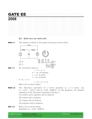
MCQ 1.1 The number of chords in the graph of the given circuit will be
(A) 3 (B) 4
(C) 5 (D) 6
SOL 1.1 No. of chords is given as
l 1b n= − +
b " no. of branches
n " no. of nodes
l " no. of chords
6b = , n 4=
l 6 4 1= − + 3=
Hence (A) is correct option.
MCQ 1.2 The Thevenin’s equivalent of a circuit operation at 5ω = rads/s, has
3.71 15.9V Voc += − %
and 2.38 0.667Z j0 Ω= − . At this frequency, the minimal
realization of the Thevenin’s impedance will have a
(A) resistor and a capacitor and an inductor
(B) resistor and a capacitor
(C) resistor and an inductor
(D) capacitor and an inductor
SOL 1.2 Hence (A) is correct option.
Impedance Zo 2.38 0.667j Ω= −
2. Page 2 GATE EE 2008 www.gatehelp.com
Brought to you by: Nodia and Company Visit us at: www.nodia.co.in
PUBLISHING FOR GATE
Constant term in impedance indicates that there is a resistance in the circuit.
Assume that only a resistance and capacitor are in the circuit, phase difference in
thevenin voltage is given as
θ ( )tan CR1
ω=− −
(Due to capacitor)
Zo R
C
j
ω
= −
So,
C
1
ω
0.667=
and R 2.38 Ω=
θ
.
.tan
0 667
1 2 381 #=− −
b l
74.34 15.9c c=− =−[
given Voc 3.71 15.9c+= −
So, there is an inductor also connected in the circuit
MCQ 1.3 A signal ( )sine tt
ωα-
is the input to a real Linear Time Invariant system. Given K
and φ are constants, the output of the system will be of the form ( )sinKe vtt
φ+β-
where
(A) β need not be equal to α but v equal to ω
(B) v need not be equal to ω but β equal to α
(C) β equal to α and v equal to ω
(D) β need not be equal to α and v need not be equal to ω
SOL 1.3 Hence (D) is correct option.
Let ( ) ( )x t X s
L
( ) ( )y t Y s
L
( ) ( )h t H s
L
So output of the system is given as
( )Y s ( ) ( )X s H s=
Now for input ( )x t τ− ( )e X s (shifting property)sL τ-
( )h t τ− ( )e H ssL τ−
So now output is '( )Y s ( ) ( )e X s e H ss s
$= τ τ- -
'( )Y s ( ) ( )e X s H ss2
= τ-
'( )Y s ( )e Y ss2
= τ-
Or '( )y t ( 2 )y t τ= −
MCQ 1.4 X is a uniformly distributed random variable that takes values between 0 and 1.
The value of { }E X3
will be
(A) 0 (B) 1/8
(C) 1/4 (D) 1/2
3. Page 3 GATE EE 2008 www.gatehelp.com
Brought to you by: Nodia and Company Visit us at: www.nodia.co.in
PUBLISHING FOR GATE
SOL 1.4 X is uniformly distributed between 0 and 1
So probability density function
( )f XX
1, 0 1
0,
x
otherwise
< <
= )
So,
{ }E X3
( )X f X dxX
3
0
1
= #
( )X dx13
0
1
= #
X
4
4
0
1
= : D
4
1=
Hence (C) is correct option
MCQ 1.5 The characteristic equation of a (3 3# ) matrix P is defined as
( )a I P 2 1 03 2
λ λ λ λ λ= − = + + + =
If I denotes identity matrix, then the inverse of matrix P will be
(A) ( )P P I22
+ + (B) ( )P P I2
+ +
(C) ( )P P I2
− + + (D) ( )P P I22
− + +
SOL 1.5 According to CAYLEY-HAMILTON Theorem every non-singular square matrix
satisfies its own characteristic equation.
Characteristic equation
( )a I Pλ λ= − 2 1 03 2
λ λ λ= + + + =
Matrix P satisfies above equation
P P P I23 2
+ + + 0=
I ( )P P P23 2
=− + +
Multiply both sides by P 1−
P 1−
( 2 )P P I2
=− + +
Hence (D) is correct option.
MCQ 1.6 If the rank of a ( )5 6# matrix Q is 4, then which one of the following statement is
correct ?
(A) Q will have four linearly independent rows and four linearly independent
columns
(B) Q will have four linearly independent rows and five linearly independent
columns
(C) QQT
will be invertible
(D) Q QT
will be invertible
SOL 1.6 Rank of a matrix is no. of linearly independent rows and columns of the matrix.
Here Rank ( )Q 4ρ =
4. Page 4 GATE EE 2008 www.gatehelp.com
Brought to you by: Nodia and Company Visit us at: www.nodia.co.in
PUBLISHING FOR GATE
So Q will have 4 linearly independent rows and flour independent columns.
Hence (A) is correct option
MCQ 1.7 A function ( )y t satisfies the following differential equation :
( )
( )
dt
dy t
y t+ ( )tδ=
where ( )tδ is the delta function. Assuming zero initial condition, and denoting the
unit step function by ( ), ( )u t y t can be of the form
(A) et
(B) e t-
(C) ( )e u tt
(D) ( )e u tt-
SOL 1.7 Given differential equation for the function
( )
( )
dt
dy t
y t+ ( )tδ=
Taking Laplace on both the sides we have,
( ) ( )sY s Y s+ 1=
( 1) ( )s Y s+ 1=
( )Y s
s 1
1=
+
Taking inverse Laplace of ( )Y s
( )y t ( )e u tt
= −
, t 0>
Hence (D) is correct option.
MCQ 1.8 The equivalent circuits of a diode, during forward biased and reverse biased
conditions, are shown in the figure.
(I)
(II)
If such a diode is used in clipper circuit of figure given above, the output voltage
V0 of the circuit will be
5. Page 5 GATE EE 2008 www.gatehelp.com
Brought to you by: Nodia and Company Visit us at: www.nodia.co.in
PUBLISHING FOR GATE
SOL 1.8 Assume the diode is in reverse bias so equivalent circuit is
Output voltage V0 10sin t
10 10
10 #ω=
+
5sin tω=
Due to resistor divider, voltage across diode 0V <D (always). So it in reverse bias
for given input.
Output, V0 5sin tω=
Hence (A) is correct option.
MCQ 1.9 Two 8-bit ADCs, one of single slope integrating type and other of successive
approximate type, take TA and TB times to convert 5 V analog input signal to
equivalent digital output. If the input analog signal is reduced to 2.5 V, the
approximate time taken by the two ADCs will respectively, be
(A) ,T TA B (B) /2,T TA B
(C) , /T T 2A B (D) /2, /2T TA B
SOL 1.9 Conversion time does not depend on input voltage so it remains same for both type
of ADCs.
Hence (A) is correct option
6. Page 6 GATE EE 2008 www.gatehelp.com
Brought to you by: Nodia and Company Visit us at: www.nodia.co.in
PUBLISHING FOR GATE
MCQ 1.10 An input device is interfaced with Intel 8085A microprocessor as memory mapped
I/O. The address of the device is 2500H. In order to input data from the device to
accumulator, the sequence of instructions will be
(A) LXI H, 2500H (B) LXI H, 2500H
MOV A, M MOV M, A
(C) LHLD 2500H (D) LHLD 2500H
MOV A, M MOV M, A
SOL 1.10 Hence ( ) is Correct Option
MCQ 1.11 Distributed winding and short chording employed in AC machines will result in
(A) increase in emf and reduction in harmonics
(B) reduction in emf and increase in harmonics
(C) increase in both emf and harmonics
(D) reduction in both emf and harmonics
SOL 1.11 Distributed winding and short chording employed in AC machine will result in
reduction of emf and harmonics.
Hence (D) is correct option.
MCQ 1.12 Three single-phase transformer are connected to form a 3-phase transformer bank.
The transformers are connected in the following manner :
The transformer connecting will be represented by
(A) Y d0 (B) Y d1
(C) Y d6 (D) Y d11
SOL 1.12 Transformer connection will be represented by Y d1.
Hence (B) is correct option.
MCQ 1.13 In a stepper motor, the detent torque means
(A) minimum of the static torque with the phase winding excited
(B) maximum of the static torque with the phase winding excited
(C) minimum of the static torque with the phase winding unexcited
(D) maximum of the static torque with the phase winding unexcited
SOL 1.13 Detent torque/Restraining toque:
The residual magnetism in the permanent magnetic material produced.
7. Page 7 GATE EE 2008 www.gatehelp.com
Brought to you by: Nodia and Company Visit us at: www.nodia.co.in
PUBLISHING FOR GATE
The detent torque is defined as the maximum load torque that can be applied to
the shaft of an unexcited motor without causing continuous rotation. In case the
motor is unexcited.
Hence (D) is correct option.
MCQ 1.14 A two machine power system is shown below. The Transmission line XY has positive
sequence impedance of Z1 Ω and zero sequence impedance of Z0 Ω
An ‘a’ phase to ground fault with zero fault impedance occurs at the centre of the
transmission line. Bus voltage at X and line current from X to F for the phase ‘a’,
are given by Va Volts and Ia amperes, respectively. Then, the impedance measured
by the ground distance relay located at the terminal X of line XY will be given by
(A) /2Z1 Ω^ h (B) /2Z0 Ω^ h
(C) ( )/2Z Z0 1 Ω+ (D) /V Ia a Ω^ h
SOL 1.14 Given for X to F section of phase ‘a’
Va -Phase voltage and Ia -phase current.
Impedance measured by ground distance,
Relay at X
Current from phase 'a'
Bus voltage
=
I
V
a
a
Ω=
Hence (D) is correct option.
MCQ 1.15 An extra high voltage transmission line of length 300 km can be approximate by
a lossless line having propagation constant .0 00127β = radians per km. Then the
percentage ratio of line length to wavelength will be given by
(A) 24.24 % (B) 12.12 %
(C) 19.05 % (D) 6.06 %
SOL 1.15 For EHV line given data is
Length of line 300= km and .0 00127β = S rad/km
wavelength λ
.
2 .2
0 00127
4947 39
β
π π= = = km
So %l
λ .
.
4947 39
300 100 0 06063 100# #= =
%l
λ
6.063=
Hence (D) is correct option.
MCQ 1.16 A-3-phase transmission line is shown in figure :
8. Page 8 GATE EE 2008 www.gatehelp.com
Brought to you by: Nodia and Company Visit us at: www.nodia.co.in
PUBLISHING FOR GATE
Voltage drop across the transmission line is given by the following equation :
V
V
V
Z
Z
Z
Z
Z
Z
Z
Z
Z
I
I
I
a
b
c
s
m
m
m
s
m
m
m
s
a
b
c
3
3
3
=
R
T
S
S
SS
R
T
S
S
SS
R
T
S
S
SS
V
X
W
W
WW
V
X
W
W
WW
V
X
W
W
WW
Shunt capacitance of the line can be neglect. If the has positive sequence impedance
of 15 Ω and zero sequence impedance of 48 Ω, then the values of Zs and Zm will be
(A) 31.5 ; 16.5Z Zs mΩ Ω= =
(B) 26 ; 11Z Zs mΩ Ω= =
(C) 16.5 ; 31.5Z Zs mΩ Ω= =
(D) 11 ; 26Z Zs mΩ Ω= =
SOL 1.16 For three phase transmission line by solving the given equation
We get,
V
V
V
a
b
c
Δ
Δ
Δ
R
T
S
S
SS
V
X
W
W
WW
( )
( )
( )
X X
X X
X X
I
I
I
0
0
0
0
0
0
2
s m
s m
s m
a
b
c
=
−
−
+
R
T
S
S
SS
R
T
S
S
SS
V
X
W
W
WW
V
X
W
W
WW
Zero sequence Impedance 2 48X Xs m= + = ...(1)
and Positive Sequence Impedance Negative Sequence Impedance=
( )X Xs m= −
15= ...(2)
By solving equation (1) and (2)
Z Xors s 26= and 11Z Xorm m =
Hence (B) is correct option.
MCQ 1.17 In the single phase voltage controller circuit shown in the figure, for what range of
triggering angle ( )α , the input voltage ( )V0 is not controllable ?
(A) 0 45< <c cα (B) 45 135< <c cα
(C) 90 180< <c cα (D) 135 180< <c cα
9. Page 9 GATE EE 2008 www.gatehelp.com
Brought to you by: Nodia and Company Visit us at: www.nodia.co.in
PUBLISHING FOR GATE
SOL 1.17 Hence (A) is correct option.
R jXL+ j50 50= +
` tanφ
R
L
50
50 1ω= = =
φ 45c=
so, firing angle ‘α’ must be higher the 45c, Thus for 0 45< < cα ,V0 is uncontrollable.
MCQ 1.18 A 3-phase voltage source inverter is operated in 180c conduction mode. Which one
of the following statements is true ?
(A) Both pole-voltage and line-voltage will have 3rd
harmonic components
(B) Pole-voltage will have 3rd
harmonic component but line-voltage will be free
from 3rd
harmonic
(C) Line-voltage will have 3rd
harmonic component but pole-voltage will be free
from 3rd
harmonic
(D) Both pole-voltage and line-voltage will be free from 3rd
harmonic components
SOL 1.18 A 3-φ voltage source inverter is operated in 180c mode in that case third harmonics
are absent in pole voltage and line voltage due to the factor ( / )cos n 6π . so both are
free from 3rd
harmonic components.
Hence (D) is correct option.
MCQ 1.19 The impulse response of a causal linear time-invariant system is given as ( )h t . Now
consider the following two statements :
Statement (I): Principle of superposition holds
Statement (II): ( )h t 0= for t 0<
Which one of the following statements is correct ?
(A) Statements (I) is correct and statement (II) is wrong
(B) Statements (II) is correct and statement (I) is wrong
(C) Both Statement (I) and Statement (II) are wrong
(D) Both Statement (I) and Statement (II) are correct
SOL 1.19 Since the given system is LTI, So principal of Superposition holds due to linearity.
For causal system ( ) 0h t = , 0t <
Both statement are correct.
Hence (D) is correct option.
MCQ 1.20 It is desired to measure parameters of 230 V/115 V, 2 kVA,
10. Page 10 GATE EE 2008 www.gatehelp.com
Brought to you by: Nodia and Company Visit us at: www.nodia.co.in
PUBLISHING FOR GATE
single-phase transformer. The following wattmeters are available in a laboratory:
W1 : 250 V, 10 A, Low Power Factor
W2 : 250 V, 5 A, Low Power Factor
W3 : 150 V, 10 A, High Power Factor
W4 : 150 V, 5 A, High Power Factor
The Wattmeters used in open circuit test and short circuit test of the transformer
will respectively be
(A) W1 and W2 (B) W2 and W4
(C) W1 and W4 (D) W2 and W3
SOL 1.20 Given: 1-φ transformer, 230 V/115 V, 2 kVA
W1 : 250 V, 10 A, Low Power Factor
W2 : 250 V, 5 A, Low Power Factor
W3 : 150 V, 10 A, High Power Factor
W4 : 150 V, 5 A, High Power Factor
In one circuit test the wattmeter W2 is used and in short circuit test of transformer
W3 is used.
Hence (D) is correct option.
Q.21 to Q.75 carry two marks each.
MCQ 1.21 The time constant for the given circuit will be
(A) 1/9 s (B) 1/4 s
(C) 4 s (D) 9 s
SOL 1.21 Time constant of the circuit can be calculated by simplifying the circuit as follows
11. Page 11 GATE EE 2008 www.gatehelp.com
Brought to you by: Nodia and Company Visit us at: www.nodia.co.in
PUBLISHING FOR GATE
Ceq
3
2= F
Equivalent Resistance
Req 3 3 6 Ω= + =
Time constant τ R Ceq eq=
6
3
2
#= 4= sec
Hence (C) is correct option
MCQ 1.22 The resonant frequency for the given circuit will be
(A) 1 rad/s (B) 2 rad/s
(C) 3 rad/s (D) 4 rad/s
SOL 1.22 Impedance of the circuit is
Z j L
R
R
j C
j C
1
1
ω= +
+ω
ω
j L
j CR
R
j CR
j CR
1 1
1
#ω
ω ω
ω
= +
+ −
−
( )
j L
C R
R j CR
1
1
2 2 2ω
ω
ω
= +
+
−
( )
C R
j L C R R j CR
1
1
2 2 2
2 2 2 2
ω
ω ω ω
=
+
+ + −
[ ( ) ]
C R
R
C R
j L C R CR
1 1
1
2 2 2 2 2 2
2 2 2 2
ω ω
ω ω ω
=
+
+
+
+ −
For resonance ( ) 0Im Z =
So, (1 )L C R2 2 2
ω ω+ CR2
ω=
12. Page 12 GATE EE 2008 www.gatehelp.com
Brought to you by: Nodia and Company Visit us at: www.nodia.co.in
PUBLISHING FOR GATE
0.1L = H, 1C = F, 1R Ω=
So, 0.1[1 (1)(1)]2
#ω ω+ (1)(1)2
ω=
1 2
ω+ 10=
& ω 39= = rad/sec
Hence (C) is correct option.
MCQ 1.23 Assuming ideal elements in the circuit shown below, the voltage Vab will be
(A) 3 V− (B) 0 V
(C) 3 V (D) 5 V
SOL 1.23 By applying KVL in the circuit
2 5V iab − + 0=
1i = A,
Vab 2 1 5#= − 3=− Volt
Hence (A) is correct option
MCQ 1.24 A capacitor consists of two metal plates each 500 500# mm2
and spaced 6 mm
apart. The space between the metal plates is filled with a glass plate of 4 mm
thickness and a layer of paper of 2 mm thickness. The relative primitivities of
the glass and paper are 8 and 2 respectively. Neglecting the fringing effect, the
capacitance will be (Given that .8 85 100
12
#ε = -
F/m )
(A) 983.3 pF (B) 1475 pF
(C) 637.7 pF (D) 9956.25 pF
SOL 1.24 Here two capacitance C1 and C2 are connected in series, so equivalent capacitance is
Ceq
C C
C C
1 2
1 2
=
+
C1
d
Ar
1
0 1ε ε=
.
4 10
8 85 10 8 500 500 10
3
12 6
#
# # # # #= −
− −
.442 5 10 11
#= −
F
13. Page 13 GATE EE 2008 www.gatehelp.com
Brought to you by: Nodia and Company Visit us at: www.nodia.co.in
PUBLISHING FOR GATE
C2
d
Ar
2
0 2ε ε=
.
2 10
8 85 10 2 500 500 10
3
12 6
#
# # # # #= −
− −
.221 25 10 11
#= −
F
Ceq
. .
. .
442 5 10 221 25 10
442 5 10 221 25 10
11 11
11 11
# #
# # #=
+− −
− −
.147 6 10 11
#= −
1476- pF
Hence (B) is correct option.
MCQ 1.25 A coil of 300 turns is wound on a non-magnetic core having a mean circumference
of 300 mm and a cross-sectional area of 300 mm2
. The inductance of the coil
corresponding to a magnetizing current of 3 A will be
(Given that 4 100
7
#μ π= -
H/m)
(A) 37.68 Hμ (B) 113.04 Hμ
(C) 3.768 Hμ (D) 1.1304 Hμ
SOL 1.25 Hence (B) is correct option.
Circumference l 300= mm
no. of turns n 300=
Cross sectional area A 300= mm2
Inductance of coil L
l
n A0
2
μ
=
( )
4 10 (300) 300 10
300 10 3
7 2 6
#
# # # #π
= −
− −
.113 04= Hμ
MCQ 1.26 In the circuit shown in the figure, the value of the current i will be given by
(A) 0.31 A (B) 1.25 A
(C) 1.75 A (D) 2.5 A
SOL 1.26 By writing node equations at node A and B
V V
1
5
1
0a a− + − 0=
2 5Va − 0=
14. Page 14 GATE EE 2008 www.gatehelp.com
Brought to you by: Nodia and Company Visit us at: www.nodia.co.in
PUBLISHING FOR GATE
& Va 2.5= V
Similarly
V V V
3
4
1
0b ab b− ++ − 0=
( )V V V
V
3
4b a b
b
− −
+ 0=
4(2.5 ) 3V V Vb b b− − + 0=
8 10Vb − 0=
& Vb 1.25= V
Current i 1.25V
1
b
= = A
Hence (B) is correct option.
MCQ 1.27 Two point charges 10Q C1 μ= and 20Q2 = mC are placed at coordinates (1,1,0)
and ( , , )1 1 0− − respectively. The total electric flux passing through a plane 0z 2=
will be
(A) 7.5 Cμ (B) 13.5 Cμ
(C) 15.0 Cμ (D) 22.5 Cμ
SOL 1.27 Hence ( ) is Correct Option
MCQ 1.28 Given a sequence [ ]x n , to generate the sequence [ ] [ ]y n x n3 4= − , which one of the
following procedures would be correct ?
(A) First delay ( )x n by 3 samples to generate [ ]z n1 , then pick every 4th
sample of
[ ]z n1 to generate [ ]z n2 , and than finally time reverse [ ]z n2 to obtain [ ]y n .
(B) First advance [ ]x n by 3 samples to generate [ ]z n1 , then pick every 4th
sample of
[ ]z n1 to generate [ ]z n2 , and then finally time reverse [ ]z n2 to obtain [ ]y n
(C) First pick every fourth sample of [ ]x n to generate [ ]v n1 , time-reverse [ ]v n1 to
obtain [ ]v n2 , and finally advance [ ]v n2 by 3 samples to obtain [ ]y n
(D) First pick every fourth sample of [ ]x n to generate [ ]v n1 , time-reverse [ ]v n1 to
obtain [ ]v n2 , and finally delay [ ]v n2 by 3 samples to obtain [ ]y n
SOL 1.28 In option (A)
[ ]z n1 [ ]x n 3= −
[ ]z n2 [4 ] [4 3]z n x n1= = −
[ ]y n [ ] [ 4 3] [3 4 ]z n x n x n2= − = − − = −Y
In option (B)
[ ]z n1 [ ]x n 3= +
[ ]z n2 [4 ] [4 3]z n x n1= = +
[ ]y n [ ] [ 4 3]z n x n2= − = − +
In option (C)
[ ]v n1 [ ]x n4=
15. Page 15 GATE EE 2008 www.gatehelp.com
Brought to you by: Nodia and Company Visit us at: www.nodia.co.in
PUBLISHING FOR GATE
[ ]v n2 [ ] [ 4 ]v n x n1= − = −
[ ]y n [ 3] [ 4( 3)] [3 4 ]v n x n x n2= + = − + = −Y
In option (D)
[ ]v n1 [ ]x n4=
[ ]v n2 [ ] [ 4 ]v n x n1= − = −
[ ]y n [ 3] [ 4( 3)] [3 4 ]v n x n x n2= − = − − = −Y
Hence (B) is correct option.
MCQ 1.29 A system with ( )x t and output ( )y t is defined by the input-output relation :
( ) ( )y t x t d
t2
τ=
3-
-
#
The system will be
(A) Casual, time-invariant and unstable
(B) Casual, time-invariant and stable
(C) non-casual, time-invariant and unstable
(D) non-casual, time-variant and unstable
SOL 1.29 Input-output relation
( )y t ( )x d
t2
τ τ=
3-
-
#
Causality :
Since ( )y t depends on ( )x t2− , So it is non-causal.
Time-variance :
( )y t ( ) ( )x d y t
t
0
2
0τ τ τ τ= − = −
3-
-
Y#
So this is time-variant.
Stability :
Output ( )y t is unbounded for an bounded input.
For example
Let ( )x τ ( )boundede= τ-
( )y t Unboundede d e
1
2 2t t
$τ= =
−3 3
τ
τ
-
-
- -
-
-
8 B#
Hence (D) is correct option.
MCQ 1.30 A signal ( ) ( )x t tsinc α= where α is a real constant ( )xsinc
( )sin
x
x
= π
π
^ h is the input
to a Linear Time Invariant system whose impulse response ( ) ( )h t tsinc β= , where
β is a real constant. If min ( , )α β denotes the minimum of α and β and similarly,
max ( , )α β denotes the maximum of α and β, and K is a constant, which one of the
following statements is true about the output of the system ?
(A) It will be of the form ( )tsincK γ where ( , )minγ α β=
(B) It will be of the form ( )tsincK γ where ( , )maxγ α β=
(C) It will be of the form ( )tsincK α
(D) It can not be a sinc type of signal
16. Page 16 GATE EE 2008 www.gatehelp.com
Brought to you by: Nodia and Company Visit us at: www.nodia.co.in
PUBLISHING FOR GATE
SOL 1.30 Output ( )y t of the given system is
( )y t ( ) ( )x t h t)=
Or ( )Y jω ( ) ( )X j H jω ω=
given that
( )x t ( )tsinc α=
( )h t ( )tsinc β=
Fourier transform of ( )x t and ( )h t are
( )X jω [ ( )] ,x t rect
2
< <F
α
π
α
ω α ω α= = −` j
( )H jω [ ( )] ,h t rect
2
< <F
β
π
β
ω β ω β= = −` j
( )Y jω rect rect
2 2
2
αβ
π
α
ω
β
ω= ` `j j
So, ( )Y jω rect
2
K
γ
ω= ` j
Where γ ( , )min α β=
And ( )y t ( )tK sinc γ=
Hence (A) is correct option.
MCQ 1.31 Let ( )x t be a periodic signal with time period T , Let ( ) ( ) ( )y t x t t x t t0 0= − + + for
some t0. The Fourier Series coefficients of ( )y t are denoted by bk . If b 0k = for all
odd k, then t0 can be equal to
(A) /T 8 (B) /T 4
(C) /T 2 (D) T2
SOL 1.31 Let ak is the Fourier series coefficient of signal ( )x t
Given ( )y t ( ) ( )x t t x t t0 0= − + +
Fourier series coefficient of ( )y t
bk e a e ajk t
k
jk t
k
0 0
= +ω ω-
bk 2 cosa k tk 0ω=
bk 0= (for all odd k)
k t0ω
2
π= , k odd"
k
T
t2
0
π
2
π=
17. Page 17 GATE EE 2008 www.gatehelp.com
Brought to you by: Nodia and Company Visit us at: www.nodia.co.in
PUBLISHING FOR GATE
For k 1= , t0
T
4
=
Hence (B) is correct option.
MCQ 1.32 ( )H z is a transfer function of a real system. When a signal [ ] (1 )x n j n
= + is the
input to such a system, the output is zero. Further, the Region of convergence
(ROC) of z1 2
1 1
− -
^ h H(z) is the entire Z-plane (except z 0= ). It can then be
inferred that ( )H z can have a minimum of
(A) one pole and one zero (B) one pole and two zeros
(C) two poles and one zero (D) two poles and two zeros
SOL 1.32 Hence ( ) is correct option.
MCQ 1.33 Given ( )
( )
X z
z a
z
2
=
−
with z a> , the residue of ( )X z zn 1-
at z a=
for n 0$ will be
(A) an 1-
(B) an
(C) nan
(D) nan 1-
SOL 1.33 Hence (D) is correct option.
Given that ( )X z
( )z a
z
2
=
−
, z a>
Residue of ( )X z zn 1-
at z a= is
( ) ( )
dz
d z a X z zn
z a
2 1
= − -
=
( )
( )dz
d z a
z a
z zn
z a
2
2
1
= −
−
-
=
dz
d zn
z a
=
=
nzn
z a
1
= -
= nan 1
= -
MCQ 1.34 Consider function ( ) ( 4)f x x2 2
= − where x is a real number. Then the function has
(A) only one minimum (B) only tow minima
(C) three minima (D) three maxima
SOL 1.34 Given function
( )f x ( )x 42 2
= −
'( )f x ( )x x2 4 22
= −
To obtain minima and maxima
'( )f x 0=
( )x x4 42
− 0=
,x x0 4 02
= − = x 2& !=
So, x 0, 2, 2= + −
''( )f x ( ) ( )x x x4 2 4 42
= + −
x12 162
= −
18. Page 18 GATE EE 2008 www.gatehelp.com
Brought to you by: Nodia and Company Visit us at: www.nodia.co.in
PUBLISHING FOR GATE
For , ''( ) ( )x f0 0 12 0 16 16 0<2
= = − =− (Maxima)
, ''( ) ( )x f2 2 12 2 16 32 0>2
=+ = − = (Minima)
, ''( ) ( )x f2 2 12 2 16 32 0>2
=− − = − − = (Minima)
So ( )f x has only two minima
Hence (B) is correct option.
MCQ 1.35 Equation e 1 0x
− = is required to be solved using Newton’s method with an initial
guess x 10 =− . Then, after one step of Newton’s method, estimate x1 of the solution
will be given by
(A) 0.71828 (B) 0.36784
(C) 0.20587 (D) 0.00000
SOL 1.35 An iterative sequence in Newton-Raphson method can obtain by following expression
xn 1+
'( )
( )
x
f x
f x
n
n
n
= −
We have to calculate x1, so n 0=
x1
'( )
( )
x
f x
f x
0
0
0
= − , Given x 10 =−
( )f x0 1e e1x 10
= − = −−
.0 63212=−
'( )f x0 e ex 10
= = −
.0 36787=
So, x1
( . )
( . )
1
0 36787
0 63212
=− −
−
.1 1 71832=− +
.0 71832=
Hence (A) is correct option
MCQ 1.36 A is m n# full rank matrix with m n> and I is identity matrix. Let matrix
' ( )A A A A1T T
= -
, Then, which one of the following statement is FALSE ?
(A) 'AA A A= (B) ( ')AA 2
(C) 'A A I= (D) ' 'AA A A=
SOL 1.36 Hence (D) is correct option
'A ( )A A AT T1
= −
( )A A AT T1 1
= − −
A I1
= −
Put 'A A I1
= −
in all option.
option (A) 'AA A A=
AA A1−
A=
19. Page 19 GATE EE 2008 www.gatehelp.com
Brought to you by: Nodia and Company Visit us at: www.nodia.co.in
PUBLISHING FOR GATE
A A= (true)
option (B) ( ')AA 2
I=
( )AA I1 2−
I=
( )I 2
I= (true)
option (C) 'A A I=
A IA1−
I=
I I= (true)
option (D) 'AA A 'A=
AA IA1−
'A A= =Y (false)
MCQ 1.37 A differential equation / ( )dx dt e u tt2
= -
, has to be solved using trapezoidal rule of
integration with a step size .h 0 01= s. Function ( )u t indicates a unit step function.
If ( )x 0 0=-
, then value of x at .t 0 01= s will be given by
(A) 0.00099 (B) 0.00495
(C) 0.0099 (D) 0.0198
SOL 1.37 Hence (C) is correct option
dt
dx ( )e u tt2
= −
x ( )e u t dtt2
= −
#
x e dtt2
0
1
= −
#
x ( )f t dt
0
1
= # ,
t .01= s
From trapezoid rule
( )f t dt
t
t nh
0
0 +
# ( ) (. )h f f
2
0 01= +6 @
( )f t dt
0
1
# . e e
2
01 .0 02
= + −
6 @, .h 01=
.0099=
MCQ 1.38 Let P be a 2 2# real orthogonal matrix and x is a real vector [ ]x ,x1 2
T
with length
( )x x x /
1
2
2
2 1 2
= + . Then, which one of the following statements is correct ?
(A) Px x# where at least one vector satisfies Px x<
(B) Px x# for all vector x
(C) Px x$ where at least one vector satisfies Px x>
(D) No relationship can be established between x and Px
SOL 1.38 P is an orthogonal matrix So PP IT
=
20. Page 20 GATE EE 2008 www.gatehelp.com
Brought to you by: Nodia and Company Visit us at: www.nodia.co.in
PUBLISHING FOR GATE
Let assume P
cos
sin
sin
cos
θ
θ
θ
θ
=
−
> H
PX
cos
sin
sin
cos
x x T
1 2
θ
θ
θ
θ
=
−
> 8H B
cos
sin
sin
cos
x
x
1
2
θ
θ
θ
θ
=
−
> >H H
cos sin
sin cos
x x
x x
1 2
1 2
θ θ
θ θ
=
−
+> H
PX ( ) ( )cos sin sin cosx x x x1 2
2
1 2
2
θ θ θ θ= − + +
x x1
2
2
2
= +
PX X=
Hence (B) is correct option.
MCQ 1.39 Let ( )x t trect 2
1
= −^ h (where ( ) 1rect x = for x2
1
2
1
# #− and zero otherwise. If
( )xsinc
( )sin
x
x
= π
π
, then the Fourier Transform of ( ) ( )x t x t+ − will be given by
(A)
2
sinc
π
ω
` j (B) 2
2
sinc
π
ω
` j
(C) 2 cos
2 2
sinc
π
ω ω
` `j j (D) sin
2 2
sinc
π
ω ω
` `j j
SOL 1.39 Given signal
( )x t rect t
2
1= −` j
So, ( )x t
1, 0 1
, elsewhere
t t
2
1
2
1
2
1
0
or# # # #
=
− −
*
Similarly
( )x t− rect t
2
1= − −` j
( )x t−
1, 1 0
, elsewhere
t t
2
1
2
1
2
1
0
or# # # #
=
− − − −
*
[ ( ) ( )]x t x tF + − ( ) ( )x t e dt x t e dtj t j t
= + −
3
3
3
3ω ω-
-
-
-
# #
( ) ( )e dt e dt1 1j t j t
0
1
1
0
= +ω ω- -
-
# #
j
e
j
ej t j t
0
1
1
0
ω ω
=
−
+
−
ω ω- -
-
; ;E E
(1 ) ( 1)
j
e
j
e1 1j j
ω ω
= − + −ω ω-
21. Page 21 GATE EE 2008 www.gatehelp.com
Brought to you by: Nodia and Company Visit us at: www.nodia.co.in
PUBLISHING FOR GATE
( ) ( )
j
e e e
j
e e e
/
/ /
/
/ /
j
j j
j
j j
2
2 2
2
2 2
ω ω
= − + −
ω
ω ω
ω
ω ω
-
- -
( )( )
j
e e e e/ / / /j j j j2 2 2 2
ω
=
− +ω ω ω ω- -
2sin cos2
2 2
$
ω
ω ω= ` `j j
2cos
2 2
sincω
π
ω= ` j
Hence (C) is correct option.
MCQ 1.40 Two perfectly matched silicon transistor are connected as shown in the figure
assuming the β of the transistors to be very high and the forward voltage drop in
diodes to be 0.7 V, the value of current I is
(A) 0 mA (B) 3.6 mA
(C) 4.3 mA (D) 5.7 mA
SOL 1.40 Hence (C) is correct option.
This is a current mirror circuit. Since β is high so ,I IC C1 2= I IB B1 2=
VB ( . )5 0 7= − +
4.3=− volt
Diode D1 is forward biased.
So, current I is,
I I IC C2 1= =
( . )
4.3
1
0 4 3
=
− −
= mA
MCQ 1.41 In the voltage doubler circuit shown in the figure, the switch ‘S ’ is closed at t 0=
22. Page 22 GATE EE 2008 www.gatehelp.com
Brought to you by: Nodia and Company Visit us at: www.nodia.co.in
PUBLISHING FOR GATE
. Assuming diodes D1 and D2 to be ideal, load resistance to be infinite and initial
capacitor voltages to be zero. The steady state voltage across capacitor C1 and C2
will be
(A) 10 , 5V VV Vc c1 2= = (B) 10 , 5V VV Vc c1 2= =−
(C) 5 , 10V VV Vc c1 2= = (D) 5 , 10V VV Vc c1 2= =−
SOL 1.41 In positive half cycle of input, diode D1 is in forward bias and D2 is off, the
equivalent circuit is
Capacitor C1 will charge upto 5+ volt. 5VC1 =+ volt
In negative halt cycle diode D1 is off and D2 is on.
Now capacitor VC2 will charge upto 10− volt in opposite direction.
Hence (D) is correct option
MCQ 1.42 The block diagrams of two of half wave rectifiers are shown in the figure. The
transfer characteristics of the rectifiers are also shown within the block.
It is desired to make full wave rectifier using above two half-wave rectifiers. The
resultants circuit will be
23. Page 23 GATE EE 2008 www.gatehelp.com
Brought to you by: Nodia and Company Visit us at: www.nodia.co.in
PUBLISHING FOR GATE
SOL 1.42 Let input Vin is a sine wave shown below
According to given transfer characteristics of rectifiers output of rectifier P is.
24. Page 24 GATE EE 2008 www.gatehelp.com
Brought to you by: Nodia and Company Visit us at: www.nodia.co.in
PUBLISHING FOR GATE
Similarly output of rectifier Q is
Output of a full wave rectifier is given as
To get output V0
( )V V VK P Q0 = − + K − gain of op-amp
So, P should connected at inverting terminal of op-amp and Q with non-inverting
terminal
Hence (D) is correct Option
MCQ 1.43 A 3-line to 8-line decoder, with active low outputs, is used to implement a 3-variable
Boolean function as shown in the figure
The simplified form of Boolean function ( , , )F A B C implemented in ‘Product of
Sum’ form will be
(A) ( )( )( )X Z X Y Z Y Z+ + + +
(B) ( )( )( )X Z X Y Z Y Z+ + + +
(C) ( )( )( )( )X Y Z X Y Z X Y Z X Y Z+ + + + + + + +
(D) ( )( )( )( )X Y Z X Y Z X Y Z X Y Z+ + + + + + + +
25. Page 25 GATE EE 2008 www.gatehelp.com
Brought to you by: Nodia and Company Visit us at: www.nodia.co.in
PUBLISHING FOR GATE
SOL 1.43 In SOP form, F is written as
F (1, 3, 5, 6)mΣ=
X Y Z X YZ XY Z XYZ= + + +
Solving from K- map
F XZ Y Z XYZ= + +
In POS form
F ( )( )( )Y Z X Z X Y Z= + + + +
since all outputs are active low so each input in above expression is complemented
F ( )( )( )Y Z X Z X Y Z= + + + +
Hence (B) is correct option.
MCQ 1.44 The truth table of monoshot shown in the figure is given in the table below :
Two monoshots, one positive edge triggered and other negative edge triggered, are
connected shown in the figure, The pulse widths of the two monoshot outputs Q1
and Q2 are TON1
and TON2
respectively.
The frequency and the duty cycle of the signal at Q1 will respectively be
(A) ,f
T T
D1
5
1
ON ON1 2
=
+
=
(B) ,f
T T
D
T T
T1
ON ON ON ON
ON
1 2 1 2
2
=
+
=
+
(C) ,f
T
D
T T
T1
ON ON ON
ON
1 1 2
1
= =
+
26. Page 26 GATE EE 2008 www.gatehelp.com
Brought to you by: Nodia and Company Visit us at: www.nodia.co.in
PUBLISHING FOR GATE
(D) ,f
T
D
T T
T1
ON ON ON
ON
2 1 2
1
= =
+
SOL 1.44 In this case
f
T T
1
ON ON1 2
=
+
and, D
T T
T
ON ON
ON
1 2
2
=
+
Hence (B) is correct option.
MCQ 1.45 The content of some of the memory location in an 8085 accumulator based system
are given below
Address Content
g g
26FE 00
26FF 01
2700 02
2701 03
2702 04
g g
The content of stack (SP), program counter (PC) and (H,L) are 2700 H, 2100 H
and 0000 H respectively. When the following sequence of instruction are executed.
2100 H: DAD SP
2101 H: PCHL
the content of (SP) and (PC) at the end of execution will be
(A) 2102 , 2700PC H SP H= = (B) 2700 , 2700PC H SP H= =
(C) 2800 , 26PC H SP FE H= = (D) 2 02 , 2702PC A H SP H= =
SOL 1.45 Given that
SP 2700 H=
PC 2100 H=
HL 0000 H=
Executing given instruction set in following steps,
DAD SP &Add register pair (SP) to HL register
HL HL SP= +
HL 0000 H 2700 H= +
HL 2700 H=
PCHL & Load program counter with HL contents
PC = HL = 2700 H
So after execution contents are,
PC = 2700 H, HL = 2700 H
27. Page 27 GATE EE 2008 www.gatehelp.com
Brought to you by: Nodia and Company Visit us at: www.nodia.co.in
PUBLISHING FOR GATE
Hence (B) is correct option.
MCQ 1.46 A waveform generator circuit using OPAMPs is shown in the figure. It produces a
triangular wave at point ‘P’ with a peak to peak voltage of 5 V for 0V Vi = .
If the voltage Vi is made .2 5+ V, the voltage waveform at point ‘P’ will become
SOL 1.46 Hence ( ) is correct option.
MCQ 1.47 A 230 V, 50 Hz, 4-pole, single-phase induction motor is rotating in the clockwise
(forward) direction at a speed of 1425 rpm. If the rotor resistance at standstill is
7.8 Ω, then the effective rotor resistance in the backward branch of the equivalent
circuit will be
(A) 2 Ω (B) 4 Ω
(C) 78 Ω (D) 156 Ω
SOL 1.47 Given: 230 V, 50 Hz, 4-Pole, 1-φ induction motor is rotating in
clock-wise(forward) direction
Ns 1425= rpm
Rotar resistance at stand still(R2) .7 8 Ω=
So
28. Page 28 GATE EE 2008 www.gatehelp.com
Brought to you by: Nodia and Company Visit us at: www.nodia.co.in
PUBLISHING FOR GATE
Ns
4
120 50 1500#= =
Slip(S ) .
1500
1500 1425 0 05= − =
Resistance in backward branch rb
S
R
2
2
=
−
.
.
2 0 05
7 8=
−
4 Ω=
Hence (B) is correct option.
MCQ 1.48 A 400 V, 50 Hz 30 hp, three-phase induction motor is drawing
50 A current at 0.8 power factor lagging. The stator and rotor copper losses are 1.5
kW and 900 W respectively. The friction and windage losses are 1050 W and the
core losses are 1200 W. The air-gap power of the motor will be
(A) 23.06 kW (B) 24.11 kW
(C) 25.01 kW (D) 26.21 kW
SOL 1.48 Given: a 400 V, 50 Hz, 30 hp, 3-φ induction motor
Current 50 A= at 0.8 p.f. lagging
Stator and rotor copper losses are 1.5 kW and 900 W
fraction and windage losses 1050 W=
Core losses 1200 W 1.2 kW==
So,
Input power in stator .3 400 50 0 8# # #=
27.71 kW=
Air gap power . . .27 71 1 5 1 2= − −
25.01 kW=
Hence (C) is correct option.
MCQ 1.49 The core of a two-winding transformer is subjected to a magnetic flux variation as
indicated in the figure.
The induced emf ( )ers in the secondary winding as a function of time will be of the
form
29. Page 29 GATE EE 2008 www.gatehelp.com
Brought to you by: Nodia and Company Visit us at: www.nodia.co.in
PUBLISHING FOR GATE
SOL 1.49 Hence (A) is correct option.
Induced emf in secondary N
dt
d
2
φ
=−
During t0 1< <−
E1 ( ) 12
dt
d
100 V
φ
=− =−
E1 and E2 are in opposition
E2 2 24E V1= =
During time t1 2< <
dt
dφ
0= , then E E 01 2= =
During .t2 2 5< <
E1 (100) 24
dt
d
V
φ
=− =−
Then
E2 0 48 V=− −
MCQ 1.50 Voltages phasors at the two terminals of a transmission line of length 70 km have
a magnitude of 1.0 per unit but are 180 degree out of phase. Assuming that the
maximum load current in the line is 1/5th
of minimum 3-phase fault current. Which one of the following transmission line
protection schemes will not pick up for this condition ?
(A) Distance protection using ohm relay with zoen-1 set to 80% of the line
impedance.
30. Page 30 GATE EE 2008 www.gatehelp.com
Brought to you by: Nodia and Company Visit us at: www.nodia.co.in
PUBLISHING FOR GATE
(B) Directional over current protection set to pick up at 1.25 times the maximum
load current
(C) Pilot relaying system with directional comparison scheme
(D) Pilot relaying system with segregated phase comparison scheme
SOL 1.50 Hence ( ) is Correct Option
MCQ 1.51 A loss less transmission line having Surge Impedance Loading (SIL) of 2280 MW
is provided with a uniformly distributed series capacitive compensation of 30%.
Then, SIL of the compensated transmission line will be
(A) 1835 MW (B) 2280 MW
(C) 2725 MW (D) 3257 MW
SOL 1.51 SIL has no effect of compensation
So SIL 2280= MW
Hence (B) is correct option.
MCQ 1.52 A loss less power system has to serve a load of 250 MW. There are tow generation (
G1 and G2) in the system with cost curves C1 and C2 respectively defined as follows
;
( ) 0.055C P P P1
2
G1 G1 G1#= +
( ) 3 0.03C P P P2
2
G2 G2 G2#= +
Where PG1 and PG2 are the MW injections from generator G1 and G2respectively.
Thus, the minimum cost dispatch will be
(A) 250 ; 0P PMW MWG1 G2= = (B) 150 ; 100P PMW MWG1 G2= =
(C) 100 ; 150P PMW MWG1 G2= = (D) 0 ; 250P PMW MWG1 G2= =
SOL 1.52 Hence (C) is correct option
Given P PG1 G2+ 250= MW ...(1)
and
( )
( )
C P
C P
1
2
G1
G2
.
.
P P
P P
0 055
3 0 03
G1 G1
2
G2 G2
2
= +
= +
4 ...(2)
from equation (2)
dP
dC1
G1
1 0.11PG1= + ...(3a)
and
dP
dC2
G2
3 0.06PG2= + ...(3b)
Since the system is loss-less
Therefore
dP
dC1
G1 dP
dC2
G2
=
So from equations (3a) and (3b)
We have 0.11 0.06P P 2G1 G− 2= ...(4)
Now solving equation (1) and (4), we get
PG1 100= MW
31. Page 31 GATE EE 2008 www.gatehelp.com
Brought to you by: Nodia and Company Visit us at: www.nodia.co.in
PUBLISHING FOR GATE
PG2 150= MW
MCQ 1.53 A loss less single machine infinite bus power system is shown below :
The synchronous generator transfers 1.0 per unit of power to the infinite bus. The
critical clearing time of circuit breaker is 0.28 s. If another identical synchronous
generator is connected in parallel to the existing generator and each generator is
scheduled to supply 0.5 per unit of power, then the critical clearing time of the
circuit breaker will
(A) reduce to 0.14 s (B) reduce but will be more than 0.14 s
(C) remain constant at 0.28 s (D) increase beyond 0.28 s
SOL 1.53 After connecting both the generators in parallel and scheduled to supply 0.5 Pu of
power results the increase in the current.
` Critical clearing time will reduced from 0.28 s but will not be less than 0.14 s for
transient stability purpose.
Hence (B) is correct option.
MCQ 1.54 Single line diagram of a 4-bus single source distribution system is shown below.
Branches , ,e e e1 2 3 and e4 have equal impedances. The load current values indicated
in the figure are in per unit.
Distribution company’s policy requires radial system operation with minimum loss.
This can be achieved by opening of the branch
(A) e1 (B) e2
(C) e3 (D) e4
32. Page 32 GATE EE 2008 www.gatehelp.com
Brought to you by: Nodia and Company Visit us at: www.nodia.co.in
PUBLISHING FOR GATE
SOL 1.54 Given that the each section has equal impedance.
Let it be R or Z , then by using the formula
line losses I R2
= /
On removing ( );e1 losses ( ) (1 2) (1 2 5)R R R1 2 2 2
= + + + + +
R R R R9 64 74= + + =
Similarly,
On removing e2;losses ( ) ( )R R R5 5 2 5 2 12 2 2
= + + + + +
R138=
lossess on removing e3 (1) ( ) ( )R R R2 5 22 2 2
= + + +
R R R1 4 49= + +
R54=
on removing e4 lossless ( ) ( )R R R2 2 1 52 2 2
= + + +
R R R4 9 25= + +
R38=
So, minimum losses are gained by removing e4 branch.
Hence (D) is correct option
MCQ 1.55 A single phase fully controlled bridge converter supplies a load drawing constant
and ripple free load current, if the triggering angle is 30c, the input power factor
will be
(A) 0.65 (B) 0.78
(C) 0.85 (D) 0.866
SOL 1.55 Given 30cα = , in a 1-φ fully bridge converter
we know that,
Power factor cosDistortion factor # α=
D.f. (Distortion factor) / 0.9I Is s(fundamental)= =
power factor . cos0 9 30# c=
.0 78=
Hence (B) is correct option
MCQ 1.56 A single-phase half controlled converter shown in the figure feeding power to highly
inductive load. The converter is operating at a firing angle of 60c.
If the firing pulses are suddenly removed, the steady state voltage ( )V0 waveform
of the converter will become
33. Page 33 GATE EE 2008 www.gatehelp.com
Brought to you by: Nodia and Company Visit us at: www.nodia.co.in
PUBLISHING FOR GATE
SOL 1.56 Output of this
Here the inductor makes T1 and T3 in ON because current passing through T1 and
34. Page 34 GATE EE 2008 www.gatehelp.com
Brought to you by: Nodia and Company Visit us at: www.nodia.co.in
PUBLISHING FOR GATE
T3 is more than the holding current.
Hence (A) is correct option
MCQ 1.57 A 220 20 ,1000V A rpm, separately excited dc motor has an armature resistance of
2.5 Ω. The motor is controlled by a step down chopper with a frequency of 1 kHz.
The input dc voltage to the chopper is 250 V. The duty cycle of the chopper for the
motor to operate at a speed of 600 rpm delivering the rated torque will be
(A) 0.518 (B) 0.608
(C) 0.852 (D) 0.902
SOL 1.57 Hence ( ) is Correct Option
MCQ 1.58 A 220 ,1400 , 40V rpm A separately excited dc motor has an armature resistance of
0.4 Ω. The motor is fed from a single phase circulating current dual converter with
an input ac line voltage of 220 V (rms). The approximate firing angles of the dual
converter for motoring operating at 50% of rated torque and 1000 rpm will be
(A) ,43 137c c (B) ,43 47c c
(C) ,39 141c c (D) ,39 51c c
SOL 1.58 Hence ( ) is Correct Option
MCQ 1.59 A single phase source inverter is feeding a purely inductive load as shown in the
figure
The inverter is operated at 50 Hz in 180c square wave mode. Assume that the load
current does not have any dc component. The peak value of the inductor current
i0 will be
(A) 6.37 A (B) 10 A
(C) 20 A (D) 40 A
SOL 1.59 Input is given as
Here load current does not have any dc component
35. Page 35 GATE EE 2008 www.gatehelp.com
Brought to you by: Nodia and Company Visit us at: www.nodia.co.in
PUBLISHING FOR GATE
`Peak current occur at ( / )π ω
` Vs L
dt
di=
200 .
dt
di0 1 #=
Here di
2 50
1
100
1
π
π= =a bk l
So di( )max
.
200
100
1
0 1
1
# #= 20 A=
Hence (C) is correct option
MCQ 1.60 A 400 V, 50 Hz, 4-pole, 1400 rpm, star connected squirrel cage induction motor has
the following parameters referred to the stator:
1.0 , ' 1.5R X X'
r s rΩ Ω= = =
Neglect stator resistance and core and rotational losses of the motor. The motor is
controlled from a 3-phase voltage source inverter with constant /V f control. The
stator line-to-line voltage(rms) and frequency to obtain the maximum torque at
starting will be :
(A) 20.6 V, 2.7 Hz (B) 133.3 V, 16.7 Hz
(C) 266.6 V, 33.3 Hz (D) 323.3 V, 40.3 Hz
SOL 1.60 Given 400 V, 50 Hz, 4-Pole, 1400 rpm star connected squirrel cage induction motor.
R 1.00 , 1.5X Xs rΩ Ω= = =l
So,
for max. torque slip
Sm
X X
R
sm rm
r
=
+ l
l
for starting torque S 1m =
Then
X Xsm rm+ l R r= l
.f L f L2 0 2m s m rπ π+ l 1=
Frequency at max. torque
fm
2 ( )L L
1
s rπ
=
+ l
Ls
.X
2 50 2 50
1 5s
# #π π
= =
L rl .
2 50
1 5
#π
=
fm
. .
50
1 5
50
1 5
1=
+ 3
50=
fm 16.7 Hz=
In const /V f control method
36. Page 36 GATE EE 2008 www.gatehelp.com
Brought to you by: Nodia and Company Visit us at: www.nodia.co.in
PUBLISHING FOR GATE
f
V
1
1
50
400 8= =
a
f
V
1
2
8=
So
V2 f 82 #=
.16 7 8#=
V2 133.3 V=
Hence (B) is correct option.
MCQ 1.61 A single phase fully controlled converter bridge is used for electrical braking of a
separately excited dc motor. The dc motor load is represented by an equivalent
circuit as shown in the figure.
Assume that the load inductance is sufficient to ensure continuous and ripple free
load current. The firing angle of the bridge for a load current of 10I0 = A will be
(A) 44c (B) 51c
(C) 129c (D) 136c
SOL 1.61 Here for continuous conduction mode, by Kirchoff’s voltage law, average load
current
V I2 150a− + 0=
Ia
V
2
150= +
10I1` = A, So
V 130=− V
cosV2 m
π
α 130=−
cos2 2 230# #
π
α 130c=−
37. Page 37 GATE EE 2008 www.gatehelp.com
Brought to you by: Nodia and Company Visit us at: www.nodia.co.in
PUBLISHING FOR GATE
α 129c=
Hence (C) is correct option.
MCQ 1.62 A three phase fully controlled bridge converter is feeding a load drawing a constant
and ripple free load current of 10 A at a firing angle of 30c. The approximate Total
harmonic Distortion (%THD) and the rms value of fundamental component of
input current will respectively be
(A) 31% and 6.8 A (B) 31% and 7.8 A
(C) 66% and 6.8 A (D) 66% and 7.8 A
SOL 1.62 Hence (B) is correct option.
Total rms current Ia 10 8.16
3
2 A#= =
Fundamental current Ia1 0.78 10 7.8 A#= =
THD 1 1
DF2= −
where
DF
.
. 0.955
I
I
0 816 10
0 78 10
a
a1
#
#= = =
` THD
.
3 %
0 955
1 1 1
2
= − =b l
MCQ 1.63 In the circuit shown in the figure, the switch is operated at a duty cycle of 0.5. A
large capacitor is connected across the load. The inductor current is assumed to be
continuous.
The average voltage across the load and the average current through the diode will
respectively be
(A) 10 V, 2 A (B) 10 V, 8 A
(C) 40 V 2 A (D) 40 V, 8 A
SOL 1.63 Hence (C) is correct option.
38. Page 38 GATE EE 2008 www.gatehelp.com
Brought to you by: Nodia and Company Visit us at: www.nodia.co.in
PUBLISHING FOR GATE
In the given diagram
when switch S is open 4 20I I VA, VL s0 = = =
when switch S is closed 0, 0I V VD 0= =
Duty cycle .0 5= so average voltage is V
1
s
δ−
Average current 2
2
0 4= + = amp
Average voltage
.
40
1 0 5
20 V=
−
=
MCQ 1.64 The transfer function of a linear time invariant system is given as
( )G s
s s3 2
1
2
=
+ +
The steady state value of the output of the system for a unit impulse input applied
at time instant t 1= will be
(A) 0 (B) 0.5
(C) 1 (D) 2
SOL 1.64 Given transfer function
( )G s
s s3 2
1
2=
+ +
Input ( )r t ( )t 1δ= −
( )R s [ ( )]t e1L s
δ= − = −
Output is given by
( )Y s ( ) ( )R s G s=
( )Y s
s s
e
3 2
s
2=
+ +
−
Steady state value of output
( )limy t
t " 3
( )limsY s
s 0
=
"
lim
s s
se
3 2s
s
0 2=
+ +"
−
0=
Hence (A) is correct option.
MCQ 1.65 The transfer functions of two compensators are given below :
( )
( )
,
( )
C
s
s
C
s
s
10
10 1
10 1
10
1 2=
+
+
=
+
+
Which one of the following statements is correct ?
(A) C1 is lead compensator and C2 is a lag compensator
(B) C1 is a lag compensator and C2 is a lead compensator
(C) Both C1 and C2 are lead compensator
(D) Both C1 and C2 are lag compensator
SOL 1.65 For C1 Phase is given by
39. Page 39 GATE EE 2008 www.gatehelp.com
Brought to you by: Nodia and Company Visit us at: www.nodia.co.in
PUBLISHING FOR GATE
C1
θ ( )tan tan
10
1 1
ω ω= −− −
a k
C1θ tan
1
10
101
2
ω
ω ω
=
+
−−
J
L
K
KK
N
P
O
OO
C1θ tan
10
9 0>1
2
ω
ω=
+
−
c m (Phase lead)
Similarly for C2, phase is
C2θ ( )tan tan
10
1 1ω ω= −− −
a k
tan
1
10
101
2
ω
ω ω
=
+
−−
J
L
K
KK
N
P
O
OO
tan
10
9 0<1
2
ω
ω=
+
−−
c m (Phase lag)
Hence (A) is correct option
MCQ 1.66 The asymptotic Bode magnitude plot of a minimum phase transfer function is
shown in the figure :
This transfer function has
(A) Three poles and one zero (B) Two poles and one zero
(C) Two poles and two zero (D) One pole and two zeros
SOL 1.66 From the given bode plot we can analyze that:
Slope 40− dB/decade"2 poles
Slope 20− dB/decade (Slope changes by 20+ dB/decade)"1 Zero
Slope 0 dB/decade (Slope changes by 20+ dB/decade)"1 Zero
So there are 2 poles and 2 zeroes in the transfer function.
Hence (C) is correct option.
MCQ 1.67 Figure shows a feedback system where K 0>
40. Page 40 GATE EE 2008 www.gatehelp.com
Brought to you by: Nodia and Company Visit us at: www.nodia.co.in
PUBLISHING FOR GATE
The range of K for which the system is stable will be given by
(A) 0 30K< < (B) 0 39K< <
(C) 0 390K< < (D) 390K >
SOL 1.67 Characteristic equation for the system
1
( )( )s s s
K
3 10
+
+ +
0=
( 3)( 10)s s s K+ + + 0=
13 30s s s K3 2
+ + + 0=
Applying Routh’s stability criteria
s3
1 30
s2
13 K
s1
( ) K
13
13 30# −
s0
K
For stability there should be no sign change in first column
So, K390 − 0> K 390<&
K 0>
0 K 90< <
Hence (C) is correct option
MCQ 1.68 The transfer function of a system is given as
s s20 100
100
2
+ +
The system is
(A) An over damped system (B) An under damped system
(C) A critically damped system (D) An unstable system
SOL 1.68 Given transfer function is
( )H s )
s s20 100
100
2=
+ +
Characteristic equation of the system is given by
s s20 1002
+ + 0=
100n
2
ω = 10n& ω = rad/sec.
2 nξω 20=
or ξ
2 10
20 1
#
= =
41. Page 41 GATE EE 2008 www.gatehelp.com
Brought to you by: Nodia and Company Visit us at: www.nodia.co.in
PUBLISHING FOR GATE
( )1ξ = so system is critically damped.
Hence (C) is correct option.
MCQ 1.69 Two sinusoidal signals ( , ) sinp t A t1 1ω ω= and ( )q t2ω are applied to X and Y inputs
of a dual channel CRO. The Lissajous figure displayed on the screen shown below :
The signal ( )q t2ω will be represented as
(A) ( ) , 2sinq t A t2 2 2 1ω ω ω ω= = (B) ( ) , /sinq t A t 22 2 2 1ω ω ω ω= =
(C) ( ) ,cosq t A t 22 2 2 1ω ω ω ω= = (D) ( ) , /cosq t A t 22 2 2 1ω ω ω ω= =
SOL 1.69 Hence (D) is correct option.
Frequency ratio
f
f
X
Y
meeting points of vertical tangents
meeting points of horizontal tangents
=
f
f
X
Y
4
2=
fY ( )f
2
1
X=
2ω /21ω=
Since the Lissajous figures are ellipse, so there is a phase difference of 90c exists
between vertical and horizontal inputs.
So ( )q t2ω ,cosA t2ω= /22 1ω ω=
MCQ 1.70 The ac bridge shown in the figure is used to measure the impedance Z .
42. Page 42 GATE EE 2008 www.gatehelp.com
Brought to you by: Nodia and Company Visit us at: www.nodia.co.in
PUBLISHING FOR GATE
If the bridge is balanced for oscillator frequency 2f = kHz, then the impedance Z
will be
(A) (260 0)j Ω+ (B) (0 200)j Ω+
(C) (260 200)j Ω− (D) (260 200)j Ω+
SOL 1.70 Impedance of different branches is given as
ZAB 500= Ω
ZBC
.
300
j F2 2 10 0 398
1
3
# # # #π μ
= + Ω
( )j200 300- − + Ω
ZAD 2 2 10 15.91 300j mH3
# # # #π Ω= +
( )j200 300- + Ω
To balance the bridge
Z ZAB CD Z ZAD BC=
500Z ( )( )j j200 300 200 300= + − +
500Z 130000=
Z (260 0)j= + Ω
Hence (A) is correct option.
Common Data for Questions 71, 72 and 73:
Consider a power system shown below:
Given that: 1 0V V j p.us1 s2= = + ;
The positive sequence impedance are
0.001 0.01Z Z j p.us1 s2= = + and 0.006 0.06Z j p.uL = +
3-phase Base 100MVA =
voltage base 400= kV(Line to Line)
Nominal system frequency 50= Hz.
43. Page 43 GATE EE 2008 www.gatehelp.com
Brought to you by: Nodia and Company Visit us at: www.nodia.co.in
PUBLISHING FOR GATE
The reference voltage for phase ‘a’ is defined as ( ) ( )cosV t V tm ω= .
A symmetrical three phase fault occurs at centre of the line, i.e. point ‘F’ at time ‘t0
’. The positive sequence impedance from source S1 to point ‘F’ equals 0.004 0.04j+
p.u. The wave form corresponding to phase ‘a’ fault current from bus X reveals that
decaying d.c. offset current is negative and in magnitude at its maximum initial
value, Assume that the negative sequence impedances are equal to postive sequence
impedance and the zero sequence impedances are three times positive sequence
impedances.
MCQ 1.71 The instant ( )t0 of the fault will be
(A) 4.682 ms (B) 9.667 ms
(C) 14.667 ms (D) 19.667 ms
SOL 1.71 Given
( )V t ( )cosV tm ω=
For symmetrical 3 φ− fault, current after the fault
( )i t ( )cosAe
Z
V t2( / )R L t m
ω α= + −−
At the instant of fault i.e t t0= , the total current ( )i t 0=
` 0 ( )cosAe
Z
V t2( / )R L t m
0
0
ω α= + −−
Ae ( / )R L t0−
( )cos
Z
V t2 m
0ω α=− −
Maximum value of the dc offset current
Ae ( / )R L t0−
( )cos
Z
V t2 m
0ω α=− −
For this to be negative max.
( )t0ω α− 0=
or t0
ω
α= ...(1)
and Z . .j0 004 0 04= +
Z 0.0401995 84.29Z c+ +α= =
` α 84.29 1.471orc= rad.
From equation (1)
t0
( )
. .
2 50
1 471 0 00468
#π
= = sec
t0 .4 682= ms
Hence (A) is correct option.
MCQ 1.72 The rms value of the component of fault current ( )If will be
(A) 3.59 kA (B) 5.07 kA
(C) 7.18 kA (D) 10.15 kA
44. Page 44 GATE EE 2008 www.gatehelp.com
Brought to you by: Nodia and Company Visit us at: www.nodia.co.in
PUBLISHING FOR GATE
SOL 1.72
Since the fault ‘F’ is at mid point of the system, therefore impedance seen is same
from both sides.
Z
2
. .0 0201 84 29c+=
Z1(Positive sequence) Z
2
= . .0 0201 84 29c+=
also Z Z Z1 2 0= = (for 3-φ fault)
` ( )I puf
. .Z
1 0
0 0201 84 29
1 0
1
c
c
c+
+
+= =
So magnitude If
(p.u.)
.49 8=
` Fault current If 49.8
3 400
100
#
#
=
7.18= kA
Hence (C) is correct option.
MCQ 1.73 Instead of the three phase fault, if a single line to ground fault occurs on phase ‘a’
at point ‘F’ with zero fault impedance, then the rms of the ac component of fault
current ( )Ix for phase ‘a’ will be
(A) 4.97 p.u (B) 7.0 p.u
(C) 14.93 p.u (D) 29.85 p.u
SOL 1.73 If fault is LG in phase ‘a’
Z1 . .Z
2
0 0201 84 29c+= =
Z2 . .Z 0 0201 84 291 c+= =
and Z0 . .Z3 0 0603 84 291 c+= =
45. Page 45 GATE EE 2008 www.gatehelp.com
Brought to you by: Nodia and Company Visit us at: www.nodia.co.in
PUBLISHING FOR GATE
Then
/I 3a I I Ia a a1 2 0= = =
` ( )I pua1
.
Z Z Z
1 0 0
1 2 0
c+=
+ +
and Ia1
( . . . )
. .
0 0201 0 0201 0 0603
1 0 9 95=
+ +
= pu
Fault Current If .I I3 29 85a a1= = = pu
So Fault current If .29 85
3 400
100
#
#
=
.4 97= kA
Hence (A) is correct option.
Common Data for Questions 74 and 75:
A 3-phase, 440 V, 50 Hz, 4-pole slip ring induction motor is feed from the rotor side
through an auto-transformer and the stator is connected to a variable resistance as
shown in the figure.
The motor is coupled to a 220 V, separately excited d.c generator feeding power
to fixed resistance of 10 Ω. Two-wattmeter method is used to measure the input
power to induction motor. The variable resistance is adjusted such the motor runs
at 1410 rpm and the following readings were recorded 1800W1 = W, 200W2 =− W.
MCQ 1.74 The speed of rotation of stator magnetic field with respect to rotor structure will be
(A) 90 rpm in the direction of rotation
(B) 90 rpm in the opposite direction of rotation
(C) 1500 rpm in the direction of rotation
(D) 1500 rpm in the opposite direction of rotation
SOL 1.74 Given 3-φ, 440 V, 50 Hz, 4-Pole slip ring motor
46. Page 46 GATE EE 2008 www.gatehelp.com
Brought to you by: Nodia and Company Visit us at: www.nodia.co.in
PUBLISHING FOR GATE
Motor is coupled to 220 V
N 1410 , 1800 , 200W Wrpm W W1 2= = =
So,
Ns
P
f120
=
1500
4
120 50 rpm#= =
Relative speed 1500 1410= −
90 rpm= in the direction of rotation.
Hence (A) is correct option.
MCQ 1.75 Neglecting all losses of both the machines, the dc generator power output and the
current through resistance ( )Rex will respectively be
(A) 96 W, 3.10 A (B) 120 W, 3.46 A
(C) 1504 W, 12.26 A (D) 1880 W, 13.71 A
SOL 1.75 Neglecting losses of both machines
Slip(S )
N
N N
s
s
= −
1500
1500 1410= − .0 06=
total power input to induction motor is
Pin 1800 200= − 1600 W=
Output power of induction motor
Pout (1 )S Pin= −
( . )1 0 06 1600= −
1504 W=
Losses are neglected so dc generator input power output power=
1504 W=
So,
I R2
1504=
I 12.26
10
1504 A= =
Hence (C) is correct option.
Linked Answer Questions: Q.76 to Q.85 carry two marks each.
Statement for Linked Answer Questions 76 and 77:
The current ( )i t sketched in the figure flows through a initially uncharged 0.3 nF
47. Page 47 GATE EE 2008 www.gatehelp.com
Brought to you by: Nodia and Company Visit us at: www.nodia.co.in
PUBLISHING FOR GATE
capacitor.
MCQ 1.76 The charge stored in the capacitor at 5t sμ= , will be
(A) 8 nC (B) 10 nC
(C) 13 nC (D) 16 nC
SOL 1.76 Charge stored at 5t μ= sec
Q ( )i t dt
0
5
= #
=area under the curve
Q =Area OABCDO
=Area (OAD)+Area(AEB)+Area(EBCD)
2 4 2 3 3 2
2
1
2
1
# # # # #= + +
4 3 6= + +
13= nC
Hence (C) is correct option
48. Page 48 GATE EE 2008 www.gatehelp.com
Brought to you by: Nodia and Company Visit us at: www.nodia.co.in
PUBLISHING FOR GATE
MCQ 1.77 The capacitor charged upto 5 ms, as per the current profile given in the figure,
is connected across an inductor of 0.6 mH. Then the value of voltage across the
capacitor after 1 sμ will approximately be
(A) 18.8 V (B) 23.5 V
(C) 23.5 V− (D) 30.6 V−
SOL 1.77 Initial voltage across capacitor
V0
C
Qo
=
. nF
nC
0 3
13=
43.33= Volt
When capacitor is connected across an inductor it will give sinusoidal esponse as
( )v tc cosV to oω=
where oω
LC
1=
. .0 3 10 0 6 10
1
9 3
# # #
= − −
2.35 106
#= rad/sec
at 1 sect μ=
So, ( )v tc 43.33 (2.35 10 1 10 )cos 6 6
# # #= −
43.33 ( 0.70)#= −
30.44=− V
Hence (D) is correct option.
Statement for Linked Answer Question 78 and 79.
The state space equation of a system is described by ,A B CX X u Y X= + =o where
X is state vector, u is input, Y is output and
, , [1 0]A B C
0
0
1
2
0
1
=
−
= == =G G
MCQ 1.78 The transfer function G(s) of this system will be
(A)
( )s
s
2+
(B)
( )s s
s
2
1
−
+
(C)
( )s
s
2−
(D)
( )s s 2
1
+
SOL 1.78 State space equation of the system is given by,
Xo A BX u= +
Y CX=
Taking Laplace transform on both sides of the equations.
( )s sX ( ) ( )A s B sX U= +
( ) ( )sI A sX− ( )B sU=
( )sX ( ) ( )sI A B sU1
= − −
( )sY` ( )C sX=
49. Page 49 GATE EE 2008 www.gatehelp.com
Brought to you by: Nodia and Company Visit us at: www.nodia.co.in
PUBLISHING FOR GATE
So ( )sY ( ) ( )C sI A B sU1
= − −
( )
( )
s
s
U
Y
T.F = ( )C sI A B1
= − −
( )sI A−
s
s0
0 0
0
1
2
= −
−> >H H
s
s0
1
2
=
−
+> H
( )sI A 1
− −
( )s s
s
s2
1 2
0
=
+
+ 1
> H
( )
( )
s s s
s
1
0
2
1
2
1=
+
+
R
T
S
S
S
SS
V
X
W
W
W
WW
Transfer function
( ) [ ]G s C sI A B1
= − − ( )
( )
s s s
s
1 0
1
0
2
1
2
1
0
1
=
+
+
R
T
S
S
S
SS
8 >
V
X
W
W
W
WW
B H
( )
( )
s s
s
1 0
2
1
2
1=
+
+
R
T
S
S
S
SS
8
V
X
W
W
W
WW
B
( )s s 2
1=
+
Hence (D) is correct option.
MCQ 1.79 A unity feedback is provided to the above system ( )G s to make it a closed loop
system as shown in figure.
For a unit step input ( )r t , the steady state error in the input will be
(A) 0 (B) 1
(C) 2 (D) 3
SOL 1.79 Steady state error is given by,
ess
1 ( ) ( )
( )
lim
G s H s
sR s
s 0
=
+"
= G
Here ( )R s [ ( )]r t
s
1L= = (Unit step input)
( )G s
( )s s 2
1=
+
( )H s 1= (Unity feed back)
So, ess
1
( 2)
1
1
lim
s s
s
s
s 0
=
+
+
"
b l
R
T
S
S
S
S
V
X
W
W
W
W
( 2) 1
( 2)
lim
s s
s s
s 0
=
+ +
+
"
= G
50. Page 50 GATE EE 2008 www.gatehelp.com
Brought to you by: Nodia and Company Visit us at: www.nodia.co.in
PUBLISHING FOR GATE
0=
Hence (A) is correct option.
Statement for Linked Answer Questions 80 and 81.
A general filter circuit is shown in the figure :
MCQ 1.80 If R R RA1 2= = and R R RB3 4= = , the circuit acts as a
(A) all pass filter (B) band pass filter
(C) high pass filter (D) low pass filter
SOL 1.80 For low frequencies,
0"ω , so
C
1 " 3
ω
Equivalent circuit is,
By applying node equation at positive and negative input terminals of op-amp.
R
v v
R
v vA i A o
1 2
− + − 0=
2vA v vi o= + ,
R R RA1 2a = =
Similarly,
R
v v
R
v 0A i A
3 4
− + − 0=
51. Page 51 GATE EE 2008 www.gatehelp.com
Brought to you by: Nodia and Company Visit us at: www.nodia.co.in
PUBLISHING FOR GATE
2vA vin= , R R RB3 4a = =
So, 0vo =
It will stop low frequency signals.
For high frequencies,
" 3ω , then 0
C
1 "
ω
Equivalent circuit is,
Output, v vo i=
So it will pass high frequency signal.
This is a high pass filter.
Hence (C) is correct option
MCQ 1.81 The output of the filter in Q.80 is given to the circuit in figure :
The gain v/s frequency characteristic of the output ( )vo will be
SOL 1.81 In Q.80 cutoff frequency of high pass filter is given by,
R C2
1
h
A
ω
π
=
52. Page 52 GATE EE 2008 www.gatehelp.com
Brought to you by: Nodia and Company Visit us at: www.nodia.co.in
PUBLISHING FOR GATE
Here given circuit is a low pass filter with cutoff frequency,
R C R C2
2
1
2
2
L
A A
ω
π π
= =
2L hω ω=
When both the circuits are connected together, equivalent circuit is,
So this is is Band pass filter, amplitude response is given by.
Hence (D) is correct option.
Statement for Linked Answer Question 82 and 83.
MCQ 1.82 A 240 V, dc shunt motor draws 15 A while supplying the rated load at a speed of
80 rad/s. The armature resistance is 0.5 Ω and the field winding resistance is 80 Ω.
The net voltage across the armature resistance at the time of plugging will be
(A) 6 V (B) 234 V
(C) 240 V (D) 474 V
SOL 1.82 Given: 240V V= , dc shunt motor
I 15 A=
Rated load at a speed 80 rad/s=
Armature Resistance .0 5 Ω=
Field winding Resistance 80 Ω=
So,
E 240 12 0.5#= −
E 234=
Vplugging V E= +
240 234= +
474 V=
Hence (D) is correct option.
MCQ 1.83 The external resistance to be added in the armature circuit to limit the armature
current to 125% of its rated value is
(A) 31.1 Ω (B) 31.9 Ω
(C) 15.1 Ω (D) 15.9 Ω]
53. Page 53 GATE EE 2008 www.gatehelp.com
Brought to you by: Nodia and Company Visit us at: www.nodia.co.in
PUBLISHING FOR GATE
SOL 1.83
External Resistance to be added in the armature circuit to limit the armature
current to 125%.
So Ia .
R R
12 1 25 474
a external
#= =
+
R Ra external+ .31 6=
Rexternal .31 1 Ω=
Hence (A) is correct option
Statement for Linked Answer Question 84 and 85.
A synchronous motor is connected to an infinite bus at 1.0 pu voltage and draws
0.6 pu current at unity power factor. Its synchronous reactance is 1.0 pu resistance
is negligible.
MCQ 1.84 The excitation voltage (E ) and load angle ( )δ will respectively be
(A) 0.8 pu and 36.86c lag (B) 0.8 pu and 36.86c lead
(C) 1.17 pu and 30.96c lead (D) 1.17 pu and 30.96c lag
SOL 1.84 A synchronous motor is connected to an infinite bus at 1.0 p.u. voltage and 0.6
p.u. current at unity power factor. Reactance is 1.0 p.u. and resistance is negligible.
So,
V 1 0c+= p.u.
Ia 0.6 0c+= p.u.
Zs 0 1 1 90R jX ja s c+= + = + = p.u.
V 1 0 0.6 0 1 90E I Za s #c c c+ + + +δ= + = −
E+δ 1.166 30.96c+= − p.u.
Excitation voltage .1 17= p.u.
Load angle ( )δ .30 96c= (lagging)
Hence (D) is correct option.
MCQ 1.85 Keeping the excitation voltage same, the load on the motor is increased such that
the motor current increases by 20%. The operating power factor will become
(A) 0.995 lagging (B) 0.995 leading
(C) 0.791 lagging (D) 0.848 leading
SOL 1.85 Hence (D) is correct option.