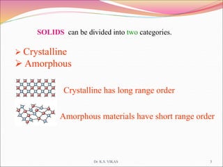
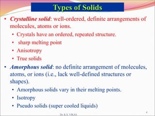
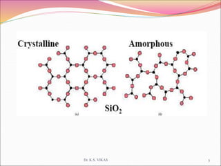
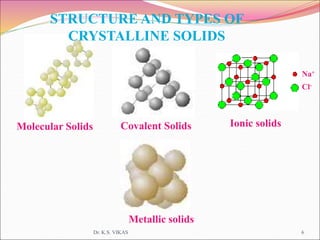
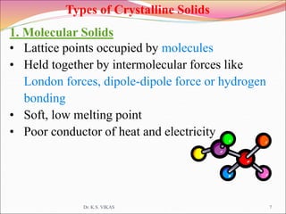
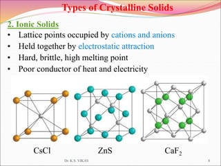
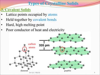
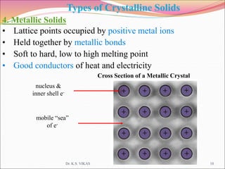
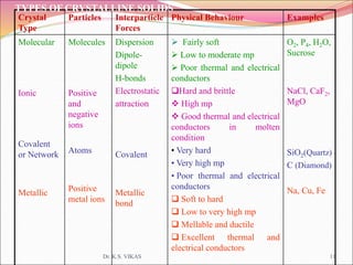
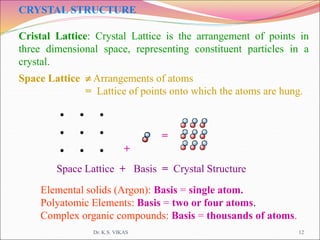
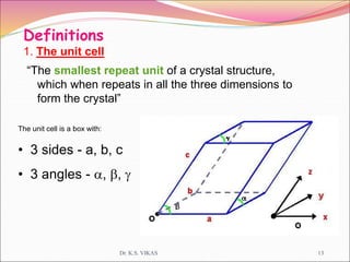
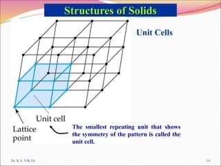
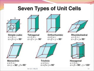
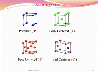
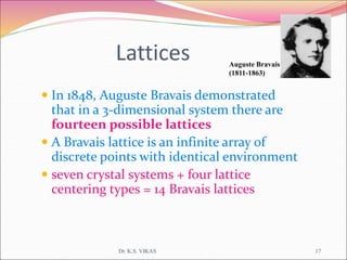
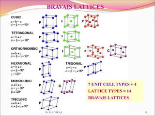
THE SOLID STATE
Dr. K.S. VIKAS 1
CONTENTS
 Types of solids
 Types of structures adopted by solids
Imperfections in solids
Dr. K.S. VIKAS 2
SOLIDS can be divided into two categories.
 Crystalline
 Amorphous
Crystalline has long range order
Amorphous materials have short range order
Dr. K.S. VIKAS 3
Dr. K.S. VIKAS
• Crystalline solid: well-ordered, definite arrangements of
molecules, atoms or ions.
• Crystals have an ordered, repeated structure.
• sharp melting point
• Anisotropy
• True solids
• Amorphous solid: no definite arrangement of molecules,
atoms, or ions (i.e., lack well-defined structures or
shapes).
• Amorphous solids vary in their melting points.
• Isotropy
• Pseudo solids (super cooled liquids)
Types of Solids
4
Dr. K.S. VIKAS 5
Molecular Solids Covalent Solids Ionic solids
Metallic solids
Na+
Cl-
STRUCTURE AND TYPES OF
CRYSTALLINE SOLIDS
Dr. K.S. VIKAS 6
Types of Crystalline Solids
1. Molecular Solids
• Lattice points occupied by molecules
• Held together by intermolecular forces like
London forces, dipole-dipole force or hydrogen
bonding
• Soft, low melting point
• Poor conductor of heat and electricity
Dr. K.S. VIKAS 7
Types of Crystalline Solids
2. Ionic Solids
• Lattice points occupied by cations and anions
• Held together by electrostatic attraction
• Hard, brittle, high melting point
• Poor conductor of heat and electricity
CsCl ZnS CaF2
Dr. K.S. VIKAS 8
Types of Crystalline Solids
3. Covalent Solids
• Lattice points occupied by atoms
• Held together by covalent bonds
• Hard, high melting point
• Poor conductor of heat and electricity
diamond graphite
carbon
atoms
Dr. K.S. VIKAS 9
Types of Crystalline Solids
4. Metallic Solids
• Lattice points occupied by positive metal ions
• Held together by metallic bonds
• Soft to hard, low to high melting point
• Good conductors of heat and electricity
Cross Section of a Metallic Crystal
nucleus &
inner shell e-
mobile “sea”
of e-
Dr. K.S. VIKAS 10
Crystal
Type
Particles Interparticle
Forces
Physical Behaviour Examples
Molecular
Ionic
Covalent
or Network
Metallic
Molecules
Positive
and
negative
ions
Atoms
Positive
metal ions
Dispersion
Dipole-
dipole
H-bonds
Electrostatic
attraction
Covalent
Metallic
bond
 Fairly soft
 Low to moderate mp
 Poor thermal and electrical
conductors
Hard and brittle
 High mp
 Good thermal and electrical
conductors in molten
condition
• Very hard
• Very high mp
• Poor thermal and electrical
conductors
 Soft to hard
 Low to very high mp
 Mellable and ductile
 Excellent thermal and
electrical conductors
O2, P4, H2O,
Sucrose
NaCl, CaF2,
MgO
SiO2(Quartz)
C (Diamond)
Na, Cu, Fe
TYPES OF CRYSTALLINE SOLIDS
Dr. K.S. VIKAS 11
CRYSTAL STRUCTURE
Cristal Lattice: Crystal Lattice is the arrangement of points in
three dimensional space, representing constituent particles in a
crystal.
Space Lattice  Arrangements of atoms
= Lattice of points onto which the atoms are hung.
Elemental solids (Argon): Basis = single atom.
Polyatomic Elements: Basis = two or four atoms.
Complex organic compounds: Basis = thousands of atoms.
+
Space Lattice + Basis = Crystal Structure
=
• • •
• • •
• • •
Dr. K.S. VIKAS 12
Definitions
1. The unit cell
“The smallest repeat unit of a crystal structure,
which when repeats in all the three dimensions to
form the crystal”
The unit cell is a box with:
• 3 sides - a, b, c
• 3 angles - , , 
Dr. K.S. VIKAS 13
Dr. K.S. VIKAS
Unit Cells
The smallest repeating unit that shows
the symmetry of the pattern is called the
unit cell.
Structures of Solids
14
TWO DIMENTIONAL UNIT CELL POSSIBILITIES OF NaCl
Na+
Cl-
Dr. K.S. VIKAS 15
Primitive ( P ) Body Centered ( I )
Face Centered ( F ) End-Centered (C )
LATTICE TYPES
Dr. K.S. VIKAS 16
Lattices
 In 1848, Auguste Bravais demonstrated
that in a 3-dimensional system there are
fourteen possible lattices
 A Bravais lattice is an infinite array of
discrete points with identical environment
 seven crystal systems + four lattice
centering types = 14 Bravais lattices
Auguste Bravais
(1811-1863)
Dr. K.S. VIKAS 17
BRAVAIS LATTICES
7 UNIT CELL TYPES + 4
LATTICE TYPES = 14
BRAVAIS LATTICES
Dr. K.S. VIKAS 18
Dr. K.S. VIKAS
• Three common types of Cubic unit cell.
• Primitive cubic, atoms at the corners of a simple cube
– each atom shared by 8 unit cells;
Common Types of Cubic Unit Cells
19
• Body-centered cubic (bcc), atoms at the corners of a
cube plus one in the center of the body of the cube,
– corner atoms shared by 8 unit cells, center atom completely
enclosed in one unit cell;
• Face-centered cubic (fcc), atoms at the corners of a
cube plus one atom in the center of each face of the cube,
– corner atoms shared by 8 unit cells, face atoms shared by 2
unit cells.
Dr. K.S. VIKAS 20
Shared by 8 unit cells
Shared by 2 unit cells
Dr. K.S. VIKAS 21
Dr. K.S. VIKAS
Unit Cells
22
Dr. K.S. VIKAS 23
Table showing Atom Fractions
in Unit Cells
Position in the
Unit Cell
Fraction in the
unit cell
Corner 1/8
Body Centre 1
Face Centre 1/2
1 atom/unit cell
(8 x 1/8 = 1)
2 atoms/unit cell
(8 x 1/8 + 1 = 2)
4 atoms/unit cell
(8 x 1/8 + 6 x 1/2 = 4)
Number of Atoms in a Unit Cell
Dr. K.S. VIKAS 24
CLOSE-PACKING OF SPHERES
Dr. K.S. VIKAS 25
CLOSE-PACKING IN TWO DIMENSIONS
SQUARE PACKING
AAA…. Type
Each particle in contact with
4 others
HEXAGONALCLOSE PACKING
ABAB…. Type
Each particle in contact with
6 others
Dr. K.S. VIKAS 26
TWO LAYERS PACKING
Dr. K.S. VIKAS 27
THREE LAYERS PACKING
Dr. K.S. VIKAS 28
Dr. K.S. VIKAS 29
Hexagonal close packing Cubic close packing
Dr. K.S. VIKAS 30
Packing Efficiency
volume of sphere
Packing Efficiency =---------------------------- X 100
Total volume of cube
Dr. K.S. VIKAS 31
(N)x (4/3 Π r3)
= --------------------- X100
a3
Dr. K.S. VIKAS 32
Packing Efficiency of Primitive Cubic Crystal
volume of sphere
Packing Efficiency =---------------------------- X 100
Total volume of cube
Dr. K.S. VIKAS 33
(N)x (4/3 Π r3)
= --------------------- X100
a3
1 x (4/3 Π r3)
= --------------------- X100
(2r)3
= 52.4%
Packing Efficiency of Body Centred Cubic
Crystal
volume of sphere
Packing Efficiency =---------------------------- X 100
Total volume of cube
Dr. K.S. VIKAS 34
(N)x (4/3 Π r3)
= --------------------- X100
a3
2 x (4/3 Π r3)
= --------------------- X100
(4/3 r)3
= 68%
Packing Efficiency of bcc, hcp & ccp
volume of sphere
Packing Efficiency =---------------------------- X 100
Total volume of cube
Dr. K.S. VIKAS 35
(N)x (4/3 Π r3)
= --------------------- X100
a3
4 x (4/3 Π r3)
= --------------------- X100
(2√2 r)3
= 74%
NON-CLOSE-PACKED STRUCTURES
68% of space is occupied
Coordination number = 8
a) Body centered cubic ( BCC ) b) Primitive cubic ( P)
52% of space is occupied
Coordination number = 6
Dr. K.S. VIKAS 36
Dr. K.S. VIKAS
Face-Centered Cubic Crystal Structure
68% of space is occupied
Hexagonal close packing &
Cubic close packing also
occupy the same space
Dr. K.S. VIKAS 38
TETRAHEDRAL HOLES
OCTAHEDRAL HOLES
TYPE OF HOLES IN CLOSE PACKING
Dr. K.S. VIKAS 39
Imperfections in Solids
or
crystal defects
Crystal Defects
• Perfect crystals do not exist; even the best crystals have
defects.
– defects are imperfections in the regular repeating
pattern
– Point defect
– Line defect
1. Point Defects
A.Vacancies
– given a perfect crystal (e.g. of Cu), an atom can be placed
on the outside of the cell to produce a vacancy (≡ □).
Dr. K.S. VIKAS 41
Types of Defects
Stoichiometric Defects:
stoichiometry is not disturbed
Non-stoichiometric Defects:
stoichiometry is disturbed
Impurity defects
Stoichiometric Defects
Schottky defect
Frenkel defect
Non-stoichiometric Defects
Metal excess defect
Metal deficiency defect
1. Stoichiometric Defects
1) Shottky Defect
– equal numbers
of anion and cation vacancies.
– may be randomly distributed, but tend
to cluster because of oppositely charged
vacancies.
– most important with alkali halides.
Dr. K.S. VIKAS 44
2) Frenkel Defect
Dislocation of cation
 cation occupies
interstitial position (void
between normal atomic
position).
Dr. K.S. VIKAS 45
Non-stoichiometric Defects
Metal excess defect
anion vacancies
excess cation
Metal deficiency defect
cation vacancies
Metal excess
defect
Anion vacancies
An anion is missing from the
crystal lattice and that place
is occupied by an electron
Color Centers (F-center; Ger:
farbenzentre)
Dr. K.S. VIKAS 47
Excess cation: in interstitial places
Metal deficiency defect cation
vacancies
3. Impurity defect
Electrical Properties
Conductors
Insulators
Semiconductors
52
Energy (Eg) required to promote electrons from the valence band to the
conduction band.
Energy Gap
Insulators
 In insulators there are no free
electrons to move throughout
the material.
 Inter-atomic bonding is ionic or
strongly covalent. The valence
electrons are tightly bonded,
highly localized and not free to
scatter throughout the crystal.
 The band-gap is large, the
valence band is full, and the
conduction band is empty.
54
• Insulators:
-- wide band gap (> 2 eV)
-- few electrons excited
across band gap
Energy
filled
band
filled
valence
band
filled
states
GAP
empty
band
conduction
55
Semiconductors
• Semiconductors:
-- narrow band gap (< 2 eV)
-- more electrons excited
across band gap
Energy
filled
band
filled
valence
band
filled
states
GAP
?
empty
band
conduction
 In semiconductors,
bonding is
predominantly covalent
(relatively weak).
 These electrons are
more easily removed by
thermal excitation.
 The band-gap is
smaller, the valence
band is full, and the
conduction band is
empty.
56
Conductors
-- for metals, empty energy states are adjacent to filled states.
• two types of band
structures for metals
• thermal energy
excites electrons
into empty higher
energy states.
- partially filled band
- empty band that
overlaps filled band
filled
band
Energy
partly
filled
band
empty
band
GAP
filled
states
Partially filled band
Energy
filled
band
filled
band
empty
band
filled
states
Overlapping bands
Semiconductors
Intrinsic semiconductors
Extrinsic Semiconductors
Intrinsic Semiconductor
materials
 Silicon and germanium each
have 4 electrons in their outer
orbital. This allows them to
form crystals.
 In a silicon lattice, all silicon
atoms covalently bond to 4
neighbors, leaving no free
electrons to conduct electric
current. This makes a silicon
crystal an insulator rather than
a conductor.
A chip, an LED and a
transistor are all made
from semiconductor
material.
Intrinsic Semiconductor
 On heating some of the covalent bonds
between silicon atoms are broken and as a
result they conduct electricity
 Semiconductors in the pure form is called
intrinsic semiconductors
Extrinsic semiconductors
 They contain some suitable impurities in their crystal
lattice. This process of adding impurities to the crystal
is called doping . They are classified into two based on
the impurity present in it.
 n-type semiconductor
 p-type semiconductor
Doping Silicon to Create n-Type
Silicon
 The "dopant” has 5 valence electrons;
silicon has 4.
 Substituting a phosphorus atom with
5 valence electrons for a silicon atom
in a silicon crystal leaves an extra,
unbonded electron that is relatively
free to move around the crystal.
Doping Silicon to Create p-Type
Silicon
 The "dopant” has 5 valence
electrons; silicon has 4.
 Substituting a boron atom
with 3 valence electrons for a
silicon atom in a silicon
crystal leaves a hole (a bond
missing an electron) that is
relatively free to move around
the crystal.
When a dopant atom with a valence of less than four is substituted
into the silicon structure, a hole is created in the structure and an
acceptor energy level is created just above the valence band. Little
energy is required to excite the holes into motion.
Magnetic Properties
Diamagnetism
Paramagnetism
Ferromagnetism
Antiferromagnetism
Ferrimagnetism
Diamagnetism
Diamagnetic materials tend
to repel flux lines weakly
All the electrons are paired
They lose their magnetism in
the absence of external
magnetic field.
Examples: water, protein, fat
Paramagnetism
 Paramagnetic substances are attracted weakly by a
magnetic field.
 They lose their magnetism in the absence of external
magnetic field.
 They have one or more unpaired electrons.
 E.g. O2, Cu2+, Fe3+, Cr3+
Ferromagnetism
 Materials that retain a
magnetization in zero field
 They are attracted strongly
by a magnetic field
 They have more unpaired
electrons.
 Examples: iron, cobalt
Antiferromagnetism
 They are expected to be
ferromagnetic but shows
zero magnetic moment.
 The magnetic moments are
oppositely arranged and
hence cancel each other.
 Many metal oxides are
antiferromagnetic
Ferrimagnetism
 They are expected to be
ferromagnetic but shows only
small magnetic moment.
 The magnetic moments are
oppositely arranged but all
magnetic moments are not
canceled.
 E.g. Fe2O3

The Solid State For Class XII

  • 1.
    THE SOLID STATE Dr.K.S. VIKAS 1
  • 2.
    CONTENTS  Types ofsolids  Types of structures adopted by solids Imperfections in solids Dr. K.S. VIKAS 2
  • 3.
    SOLIDS can bedivided into two categories.  Crystalline  Amorphous Crystalline has long range order Amorphous materials have short range order Dr. K.S. VIKAS 3
  • 4.
    Dr. K.S. VIKAS •Crystalline solid: well-ordered, definite arrangements of molecules, atoms or ions. • Crystals have an ordered, repeated structure. • sharp melting point • Anisotropy • True solids • Amorphous solid: no definite arrangement of molecules, atoms, or ions (i.e., lack well-defined structures or shapes). • Amorphous solids vary in their melting points. • Isotropy • Pseudo solids (super cooled liquids) Types of Solids 4
  • 5.
  • 6.
    Molecular Solids CovalentSolids Ionic solids Metallic solids Na+ Cl- STRUCTURE AND TYPES OF CRYSTALLINE SOLIDS Dr. K.S. VIKAS 6
  • 7.
    Types of CrystallineSolids 1. Molecular Solids • Lattice points occupied by molecules • Held together by intermolecular forces like London forces, dipole-dipole force or hydrogen bonding • Soft, low melting point • Poor conductor of heat and electricity Dr. K.S. VIKAS 7
  • 8.
    Types of CrystallineSolids 2. Ionic Solids • Lattice points occupied by cations and anions • Held together by electrostatic attraction • Hard, brittle, high melting point • Poor conductor of heat and electricity CsCl ZnS CaF2 Dr. K.S. VIKAS 8
  • 9.
    Types of CrystallineSolids 3. Covalent Solids • Lattice points occupied by atoms • Held together by covalent bonds • Hard, high melting point • Poor conductor of heat and electricity diamond graphite carbon atoms Dr. K.S. VIKAS 9
  • 10.
    Types of CrystallineSolids 4. Metallic Solids • Lattice points occupied by positive metal ions • Held together by metallic bonds • Soft to hard, low to high melting point • Good conductors of heat and electricity Cross Section of a Metallic Crystal nucleus & inner shell e- mobile “sea” of e- Dr. K.S. VIKAS 10
  • 11.
    Crystal Type Particles Interparticle Forces Physical BehaviourExamples Molecular Ionic Covalent or Network Metallic Molecules Positive and negative ions Atoms Positive metal ions Dispersion Dipole- dipole H-bonds Electrostatic attraction Covalent Metallic bond  Fairly soft  Low to moderate mp  Poor thermal and electrical conductors Hard and brittle  High mp  Good thermal and electrical conductors in molten condition • Very hard • Very high mp • Poor thermal and electrical conductors  Soft to hard  Low to very high mp  Mellable and ductile  Excellent thermal and electrical conductors O2, P4, H2O, Sucrose NaCl, CaF2, MgO SiO2(Quartz) C (Diamond) Na, Cu, Fe TYPES OF CRYSTALLINE SOLIDS Dr. K.S. VIKAS 11
  • 12.
    CRYSTAL STRUCTURE Cristal Lattice:Crystal Lattice is the arrangement of points in three dimensional space, representing constituent particles in a crystal. Space Lattice  Arrangements of atoms = Lattice of points onto which the atoms are hung. Elemental solids (Argon): Basis = single atom. Polyatomic Elements: Basis = two or four atoms. Complex organic compounds: Basis = thousands of atoms. + Space Lattice + Basis = Crystal Structure = • • • • • • • • • Dr. K.S. VIKAS 12
  • 13.
    Definitions 1. The unitcell “The smallest repeat unit of a crystal structure, which when repeats in all the three dimensions to form the crystal” The unit cell is a box with: • 3 sides - a, b, c • 3 angles - , ,  Dr. K.S. VIKAS 13
  • 14.
    Dr. K.S. VIKAS UnitCells The smallest repeating unit that shows the symmetry of the pattern is called the unit cell. Structures of Solids 14
  • 15.
    TWO DIMENTIONAL UNITCELL POSSIBILITIES OF NaCl Na+ Cl- Dr. K.S. VIKAS 15
  • 16.
    Primitive ( P) Body Centered ( I ) Face Centered ( F ) End-Centered (C ) LATTICE TYPES Dr. K.S. VIKAS 16
  • 17.
    Lattices  In 1848,Auguste Bravais demonstrated that in a 3-dimensional system there are fourteen possible lattices  A Bravais lattice is an infinite array of discrete points with identical environment  seven crystal systems + four lattice centering types = 14 Bravais lattices Auguste Bravais (1811-1863) Dr. K.S. VIKAS 17
  • 18.
    BRAVAIS LATTICES 7 UNITCELL TYPES + 4 LATTICE TYPES = 14 BRAVAIS LATTICES Dr. K.S. VIKAS 18
  • 19.
    Dr. K.S. VIKAS •Three common types of Cubic unit cell. • Primitive cubic, atoms at the corners of a simple cube – each atom shared by 8 unit cells; Common Types of Cubic Unit Cells 19 • Body-centered cubic (bcc), atoms at the corners of a cube plus one in the center of the body of the cube, – corner atoms shared by 8 unit cells, center atom completely enclosed in one unit cell; • Face-centered cubic (fcc), atoms at the corners of a cube plus one atom in the center of each face of the cube, – corner atoms shared by 8 unit cells, face atoms shared by 2 unit cells.
  • 20.
  • 21.
    Shared by 8unit cells Shared by 2 unit cells Dr. K.S. VIKAS 21
  • 22.
  • 23.
    Dr. K.S. VIKAS23 Table showing Atom Fractions in Unit Cells Position in the Unit Cell Fraction in the unit cell Corner 1/8 Body Centre 1 Face Centre 1/2
  • 24.
    1 atom/unit cell (8x 1/8 = 1) 2 atoms/unit cell (8 x 1/8 + 1 = 2) 4 atoms/unit cell (8 x 1/8 + 6 x 1/2 = 4) Number of Atoms in a Unit Cell Dr. K.S. VIKAS 24
  • 25.
  • 26.
    CLOSE-PACKING IN TWODIMENSIONS SQUARE PACKING AAA…. Type Each particle in contact with 4 others HEXAGONALCLOSE PACKING ABAB…. Type Each particle in contact with 6 others Dr. K.S. VIKAS 26
  • 27.
  • 28.
  • 29.
  • 30.
    Hexagonal close packingCubic close packing Dr. K.S. VIKAS 30
  • 31.
    Packing Efficiency volume ofsphere Packing Efficiency =---------------------------- X 100 Total volume of cube Dr. K.S. VIKAS 31 (N)x (4/3 Π r3) = --------------------- X100 a3
  • 32.
  • 33.
    Packing Efficiency ofPrimitive Cubic Crystal volume of sphere Packing Efficiency =---------------------------- X 100 Total volume of cube Dr. K.S. VIKAS 33 (N)x (4/3 Π r3) = --------------------- X100 a3 1 x (4/3 Π r3) = --------------------- X100 (2r)3 = 52.4%
  • 34.
    Packing Efficiency ofBody Centred Cubic Crystal volume of sphere Packing Efficiency =---------------------------- X 100 Total volume of cube Dr. K.S. VIKAS 34 (N)x (4/3 Π r3) = --------------------- X100 a3 2 x (4/3 Π r3) = --------------------- X100 (4/3 r)3 = 68%
  • 35.
    Packing Efficiency ofbcc, hcp & ccp volume of sphere Packing Efficiency =---------------------------- X 100 Total volume of cube Dr. K.S. VIKAS 35 (N)x (4/3 Π r3) = --------------------- X100 a3 4 x (4/3 Π r3) = --------------------- X100 (2√2 r)3 = 74%
  • 36.
    NON-CLOSE-PACKED STRUCTURES 68% ofspace is occupied Coordination number = 8 a) Body centered cubic ( BCC ) b) Primitive cubic ( P) 52% of space is occupied Coordination number = 6 Dr. K.S. VIKAS 36
  • 37.
    Dr. K.S. VIKAS Face-CenteredCubic Crystal Structure 68% of space is occupied Hexagonal close packing & Cubic close packing also occupy the same space
  • 38.
  • 39.
    TETRAHEDRAL HOLES OCTAHEDRAL HOLES TYPEOF HOLES IN CLOSE PACKING Dr. K.S. VIKAS 39
  • 40.
  • 41.
    Crystal Defects • Perfectcrystals do not exist; even the best crystals have defects. – defects are imperfections in the regular repeating pattern – Point defect – Line defect 1. Point Defects A.Vacancies – given a perfect crystal (e.g. of Cu), an atom can be placed on the outside of the cell to produce a vacancy (≡ □). Dr. K.S. VIKAS 41
  • 42.
    Types of Defects StoichiometricDefects: stoichiometry is not disturbed Non-stoichiometric Defects: stoichiometry is disturbed Impurity defects
  • 43.
    Stoichiometric Defects Schottky defect Frenkeldefect Non-stoichiometric Defects Metal excess defect Metal deficiency defect
  • 44.
    1. Stoichiometric Defects 1)Shottky Defect – equal numbers of anion and cation vacancies. – may be randomly distributed, but tend to cluster because of oppositely charged vacancies. – most important with alkali halides. Dr. K.S. VIKAS 44
  • 45.
    2) Frenkel Defect Dislocationof cation  cation occupies interstitial position (void between normal atomic position). Dr. K.S. VIKAS 45
  • 46.
    Non-stoichiometric Defects Metal excessdefect anion vacancies excess cation Metal deficiency defect cation vacancies
  • 47.
    Metal excess defect Anion vacancies Ananion is missing from the crystal lattice and that place is occupied by an electron Color Centers (F-center; Ger: farbenzentre) Dr. K.S. VIKAS 47
  • 48.
    Excess cation: ininterstitial places
  • 49.
    Metal deficiency defectcation vacancies
  • 50.
  • 51.
  • 52.
  • 53.
    Energy (Eg) requiredto promote electrons from the valence band to the conduction band. Energy Gap
  • 54.
    Insulators  In insulatorsthere are no free electrons to move throughout the material.  Inter-atomic bonding is ionic or strongly covalent. The valence electrons are tightly bonded, highly localized and not free to scatter throughout the crystal.  The band-gap is large, the valence band is full, and the conduction band is empty. 54 • Insulators: -- wide band gap (> 2 eV) -- few electrons excited across band gap Energy filled band filled valence band filled states GAP empty band conduction
  • 55.
    55 Semiconductors • Semiconductors: -- narrowband gap (< 2 eV) -- more electrons excited across band gap Energy filled band filled valence band filled states GAP ? empty band conduction  In semiconductors, bonding is predominantly covalent (relatively weak).  These electrons are more easily removed by thermal excitation.  The band-gap is smaller, the valence band is full, and the conduction band is empty.
  • 56.
    56 Conductors -- for metals,empty energy states are adjacent to filled states. • two types of band structures for metals • thermal energy excites electrons into empty higher energy states. - partially filled band - empty band that overlaps filled band filled band Energy partly filled band empty band GAP filled states Partially filled band Energy filled band filled band empty band filled states Overlapping bands
  • 57.
  • 58.
    Intrinsic Semiconductor materials  Siliconand germanium each have 4 electrons in their outer orbital. This allows them to form crystals.  In a silicon lattice, all silicon atoms covalently bond to 4 neighbors, leaving no free electrons to conduct electric current. This makes a silicon crystal an insulator rather than a conductor. A chip, an LED and a transistor are all made from semiconductor material.
  • 59.
    Intrinsic Semiconductor  Onheating some of the covalent bonds between silicon atoms are broken and as a result they conduct electricity  Semiconductors in the pure form is called intrinsic semiconductors
  • 60.
    Extrinsic semiconductors  Theycontain some suitable impurities in their crystal lattice. This process of adding impurities to the crystal is called doping . They are classified into two based on the impurity present in it.  n-type semiconductor  p-type semiconductor
  • 61.
    Doping Silicon toCreate n-Type Silicon  The "dopant” has 5 valence electrons; silicon has 4.  Substituting a phosphorus atom with 5 valence electrons for a silicon atom in a silicon crystal leaves an extra, unbonded electron that is relatively free to move around the crystal.
  • 62.
    Doping Silicon toCreate p-Type Silicon  The "dopant” has 5 valence electrons; silicon has 4.  Substituting a boron atom with 3 valence electrons for a silicon atom in a silicon crystal leaves a hole (a bond missing an electron) that is relatively free to move around the crystal.
  • 63.
    When a dopantatom with a valence of less than four is substituted into the silicon structure, a hole is created in the structure and an acceptor energy level is created just above the valence band. Little energy is required to excite the holes into motion.
  • 64.
  • 65.
    Diamagnetism Diamagnetic materials tend torepel flux lines weakly All the electrons are paired They lose their magnetism in the absence of external magnetic field. Examples: water, protein, fat
  • 66.
    Paramagnetism  Paramagnetic substancesare attracted weakly by a magnetic field.  They lose their magnetism in the absence of external magnetic field.  They have one or more unpaired electrons.  E.g. O2, Cu2+, Fe3+, Cr3+
  • 67.
    Ferromagnetism  Materials thatretain a magnetization in zero field  They are attracted strongly by a magnetic field  They have more unpaired electrons.  Examples: iron, cobalt
  • 68.
    Antiferromagnetism  They areexpected to be ferromagnetic but shows zero magnetic moment.  The magnetic moments are oppositely arranged and hence cancel each other.  Many metal oxides are antiferromagnetic
  • 69.
    Ferrimagnetism  They areexpected to be ferromagnetic but shows only small magnetic moment.  The magnetic moments are oppositely arranged but all magnetic moments are not canceled.  E.g. Fe2O3