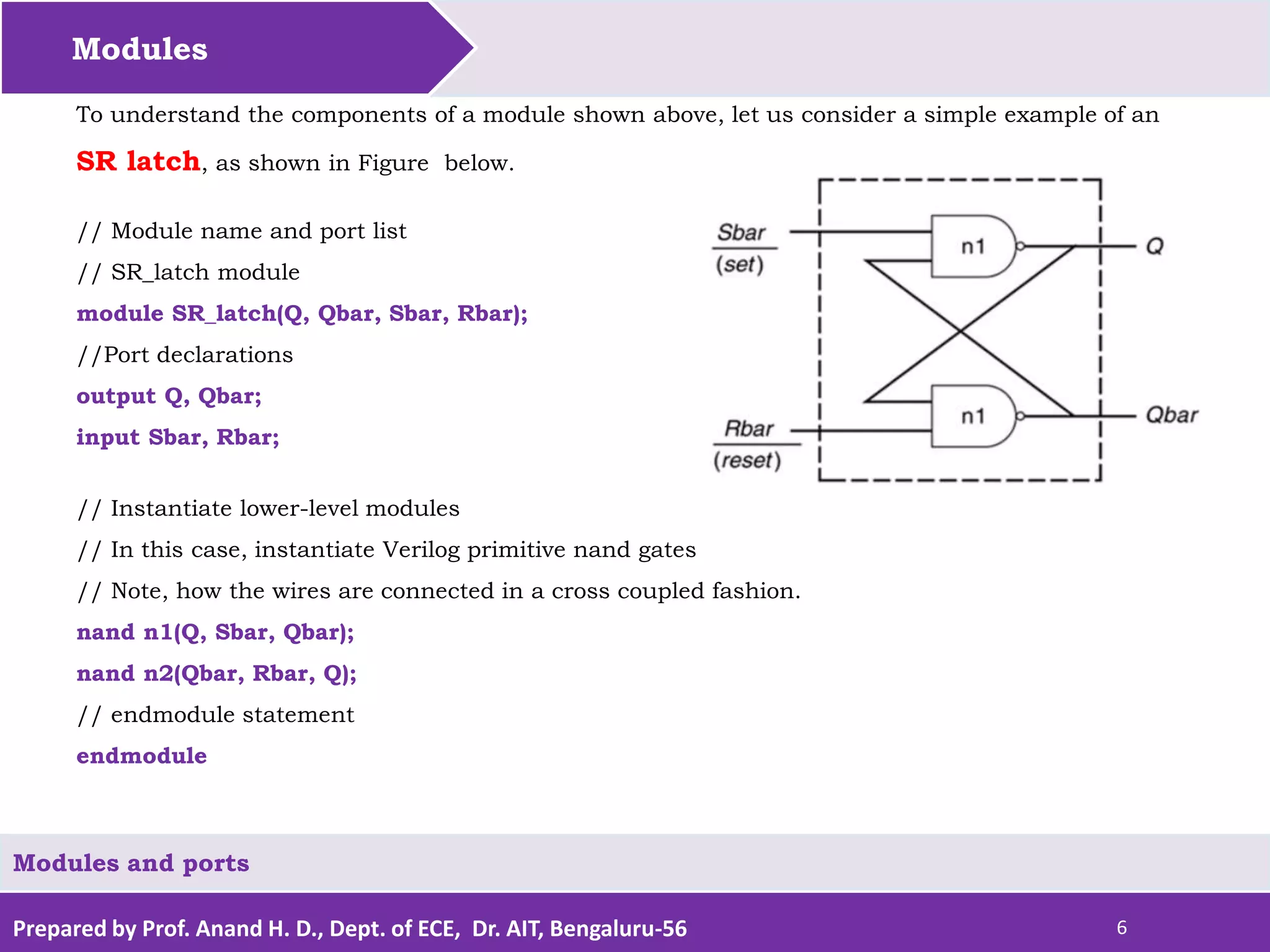
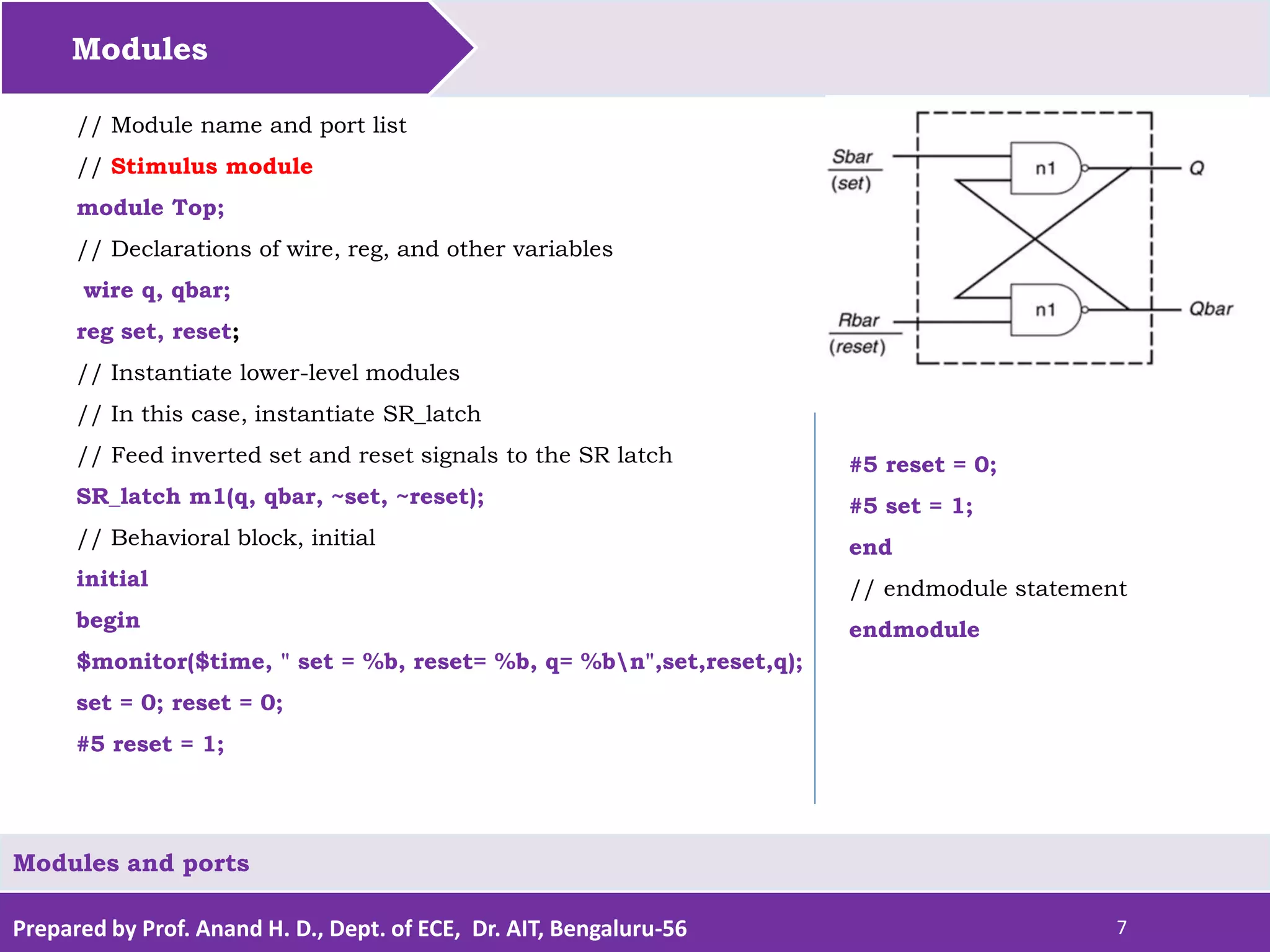
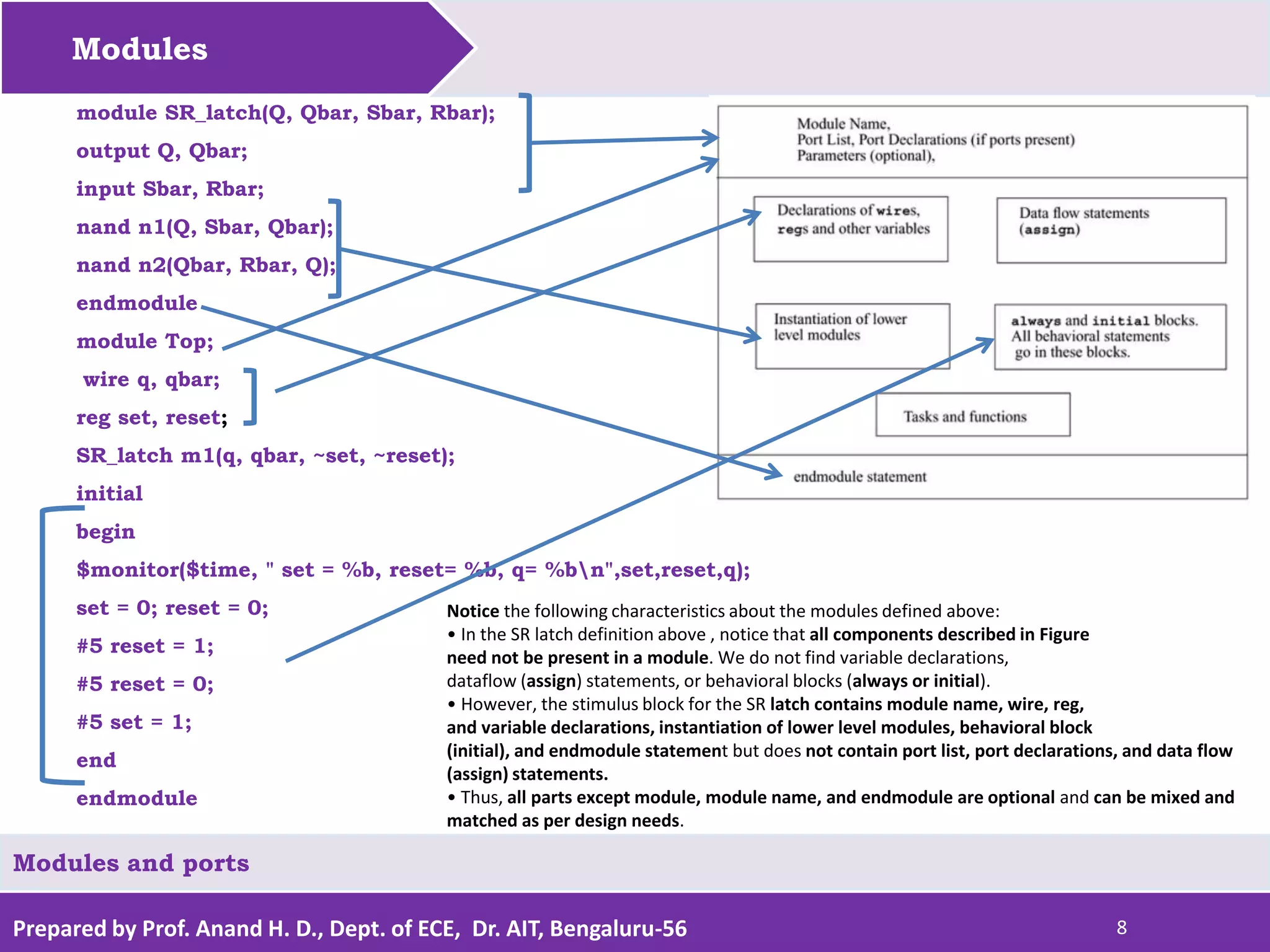
Download to read offline


![Prepared by Prof. Anand H. D., Dept. of ECE, Dr. AIT, Bengaluru-56 12
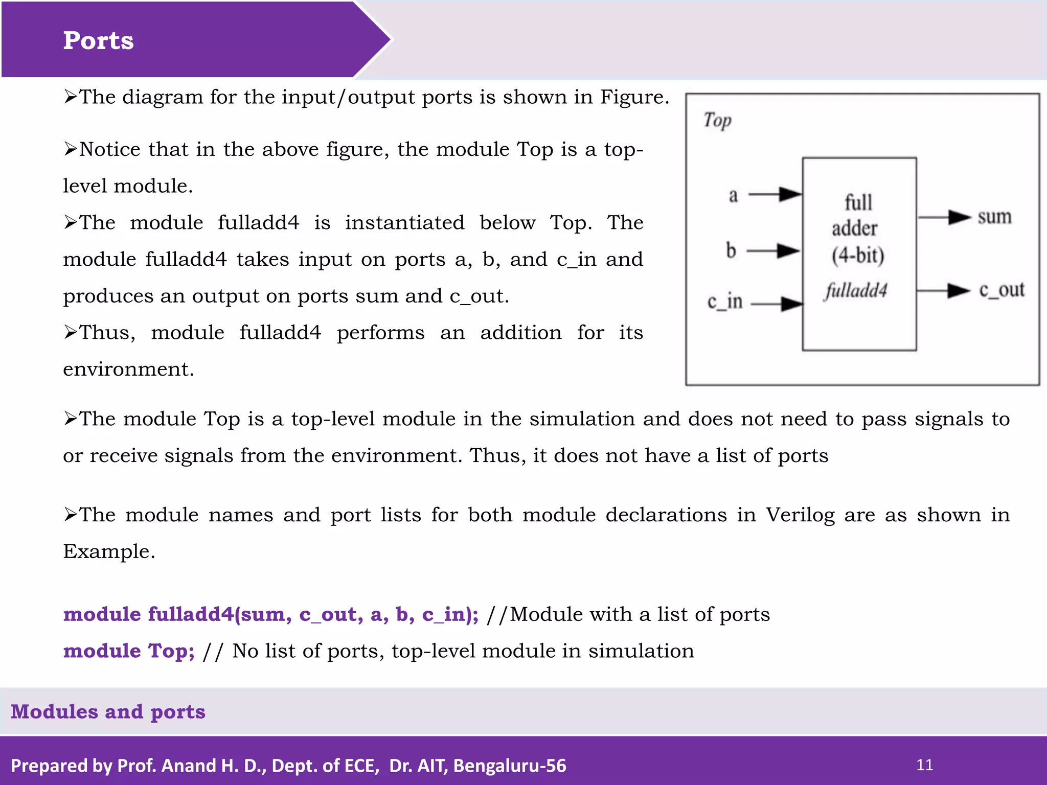
Ports
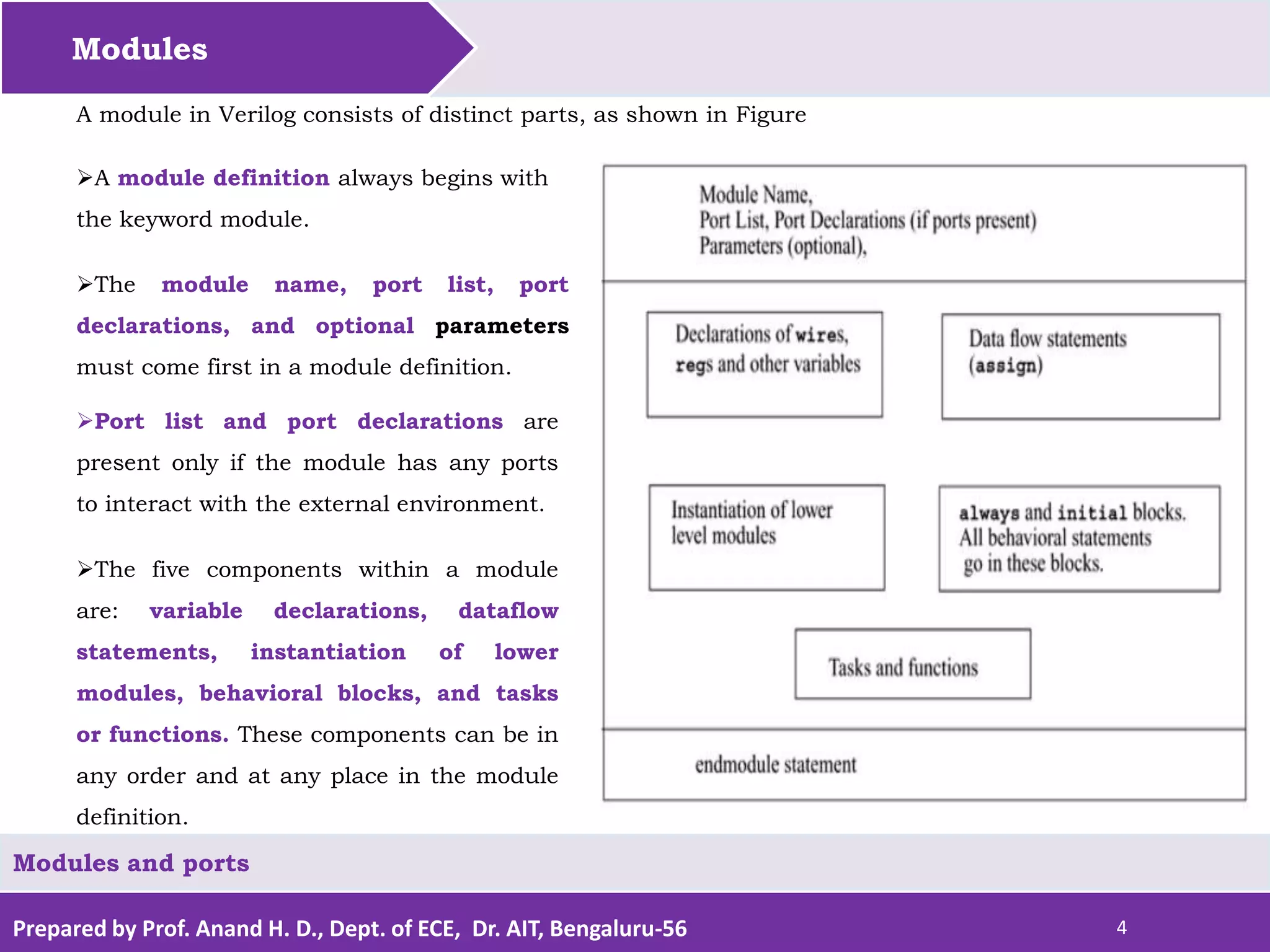
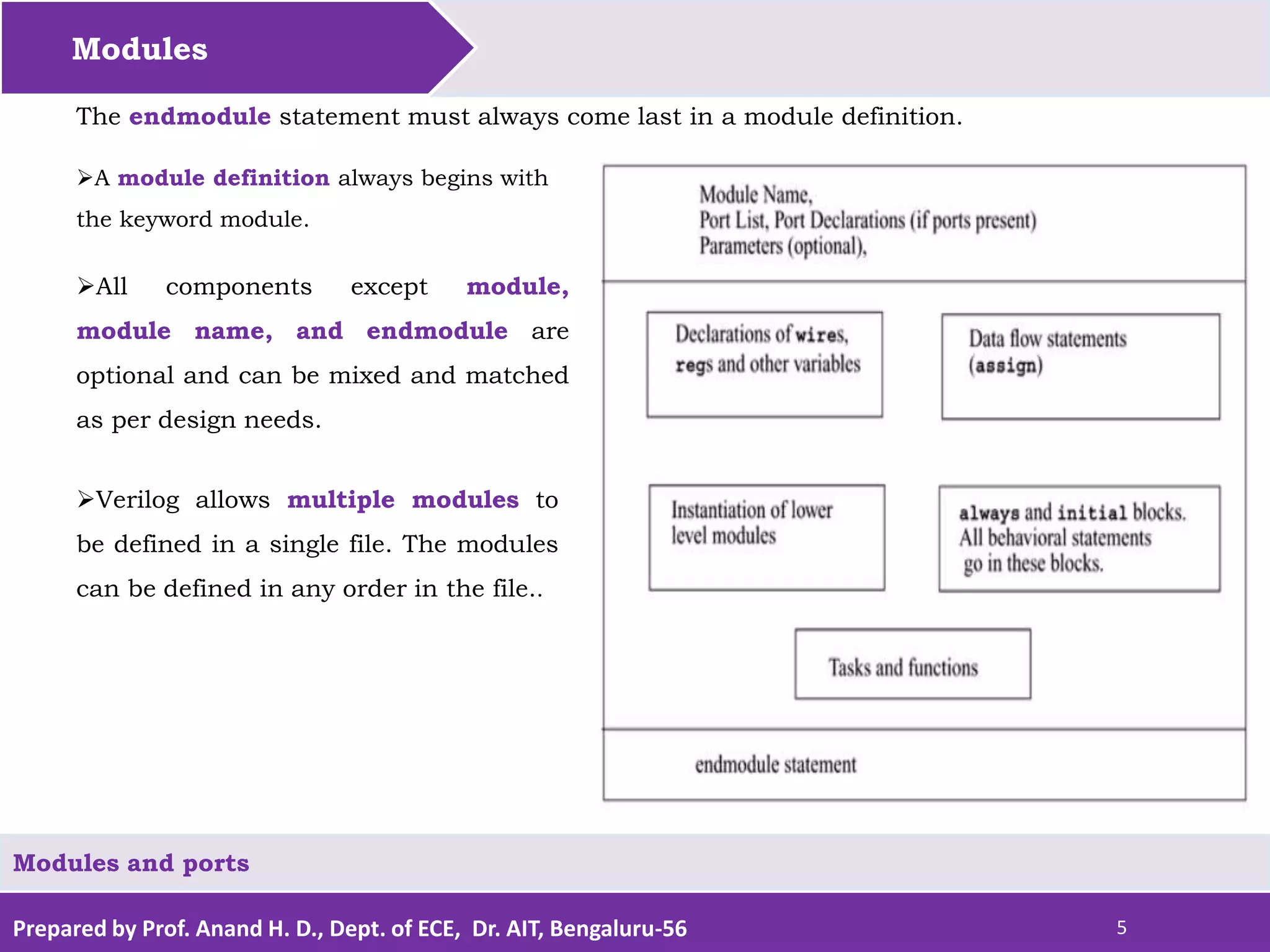
Modules and ports
2. Port Declaration
All ports in the list of ports must be declared in the module. Ports can be declared as follows:
Each port in the port list is defined as input,
output, or inout, based on the direction of the
port signal. Thus, for the example of the fulladd4
in Example, the port declarations will be as
shown
module fulladd4(sum, c_out, a, b, c_in);
//Begin port declarations section
output[3:0] sum;
output c_cout;
input [3:0] a, b;
input c_in;
//End port declarations section
...
<module internals>
...
endmodule
Note that all port declarations are implicitly declared as wire
in Verilog. Thus, if a port is intended to be a wire, it is
sufficient to declare it as output, input, or inout. Input or
inout ports are normally declared as wires.
However, if output ports hold their value, they must be
declared as reg. For example, in the definition of DFF, in
Example, we wanted the output q to retain its value until
the next clock edge. The port declarations for DFF will look
as shown in following Example](https://image.slidesharecdn.com/modulesandports-210510085037/75/Modules-and-ports-in-Verilog-HDL-12-2048.jpg)

![Prepared by Prof. Anand H. D., Dept. of ECE, Dr. AIT, Bengaluru-56 14
Ports
Modules and ports
Following Example shows this alternate syntax.
This syntax avoids the duplication of naming the ports in both the module definition
statement and the module port list definitions.
If a port is declared but no data type is specified, then, under specific circumstances, the
signal will default to a wire data type.
Example ANSI C Style Port Declaration Syntax
module fulladd4(output reg [3:0] sum,
output reg c_out,
input [3:0] a, b, //wire by default
input c_in); //wire by default
...
<module internals>
...
endmodule
module fulladd4(sum, c_out, a, b, c_in);
//Begin port declarations section
output[3:0] sum;
output c_cout;
input [3:0] a, b;
input c_in;
//End port declarations section
...
<module internals>
...
endmodule](https://image.slidesharecdn.com/modulesandports-210510085037/75/Modules-and-ports-in-Verilog-HDL-14-2048.jpg)
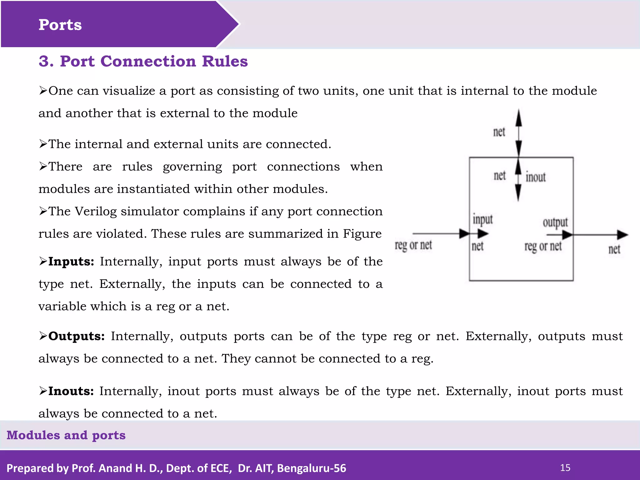
![Prepared by Prof. Anand H. D., Dept. of ECE, Dr. AIT, Bengaluru-56 16
Ports
Modules and ports
Width matching
It is legal to connect internal and external items of different sizes when making intermodule
port connections. However, a warning is typically issued that the widths do not match.
Unconnected ports
Verilog allows ports to remain unconnected.
For example, certain output ports might be simply for debugging, and you might not be
interested in connecting them to the external signals.
You can let a port remain unconnected by instantiating a module as shown below.
fulladd4 fa0(SUM, , A, B, C_IN); // Output port c_out is unconnected
module Top;
//Declare connection variables
reg [3:0]A,B;
reg C_IN;
reg [3:0] SUM;
wire C_OUT;
//Instantiate fulladd4, call it fa0
fulladd4 fa0(SUM, C_OUT, A, B, C_IN);
.
<stimulus>
.
endmodule
/* Illegal connection because output port sum in
module fulladd4 is connected to a register variable
SUM in module Top. */
Illegal Port Connection](https://image.slidesharecdn.com/modulesandports-210510085037/75/Modules-and-ports-in-Verilog-HDL-16-2048.jpg)

![Prepared by Prof. Anand H. D., Dept. of ECE, Dr. AIT, Bengaluru-56 18
Ports
Modules and ports
Connection by Ordered List
module Top;
//Declare connection variables
reg [3:0]A,B;
reg C_IN;
wire [3:0] SUM;
wire C_OUT;
//Instantiate fulladd4, call it fa_ordered.
//Signals are connected to ports in order
//(by position)
fulladd4 fa_ordered(SUM, C_OUT, A, B, C_IN);
...
<stimulus>
...
endmodule
module fulladd4(sum, c_out, a, b, c_in);
//Begin port declarations section
output[3:0] sum;
output c_cout;
input [3:0] a, b;
input c_in;
//End port declarations section
...
<module internals>
...
endmodule
Notice that the external signals SUM, C_OUT, A, B, and
C_IN appear in exactly the same order as the ports sum,
c_out, a, b, and c_in in module definition of fulladd4..](https://image.slidesharecdn.com/modulesandports-210510085037/75/Modules-and-ports-in-Verilog-HDL-18-2048.jpg)


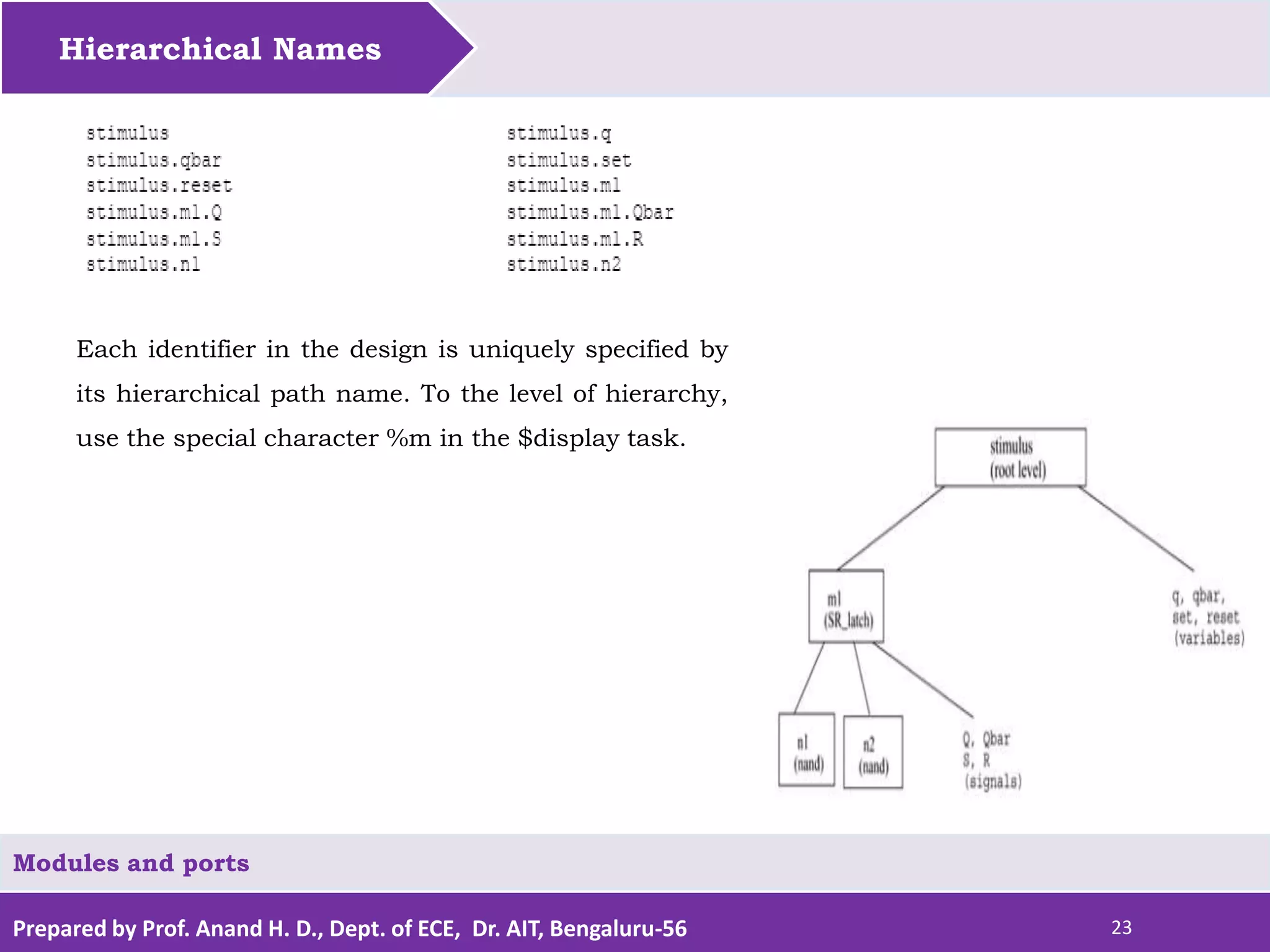
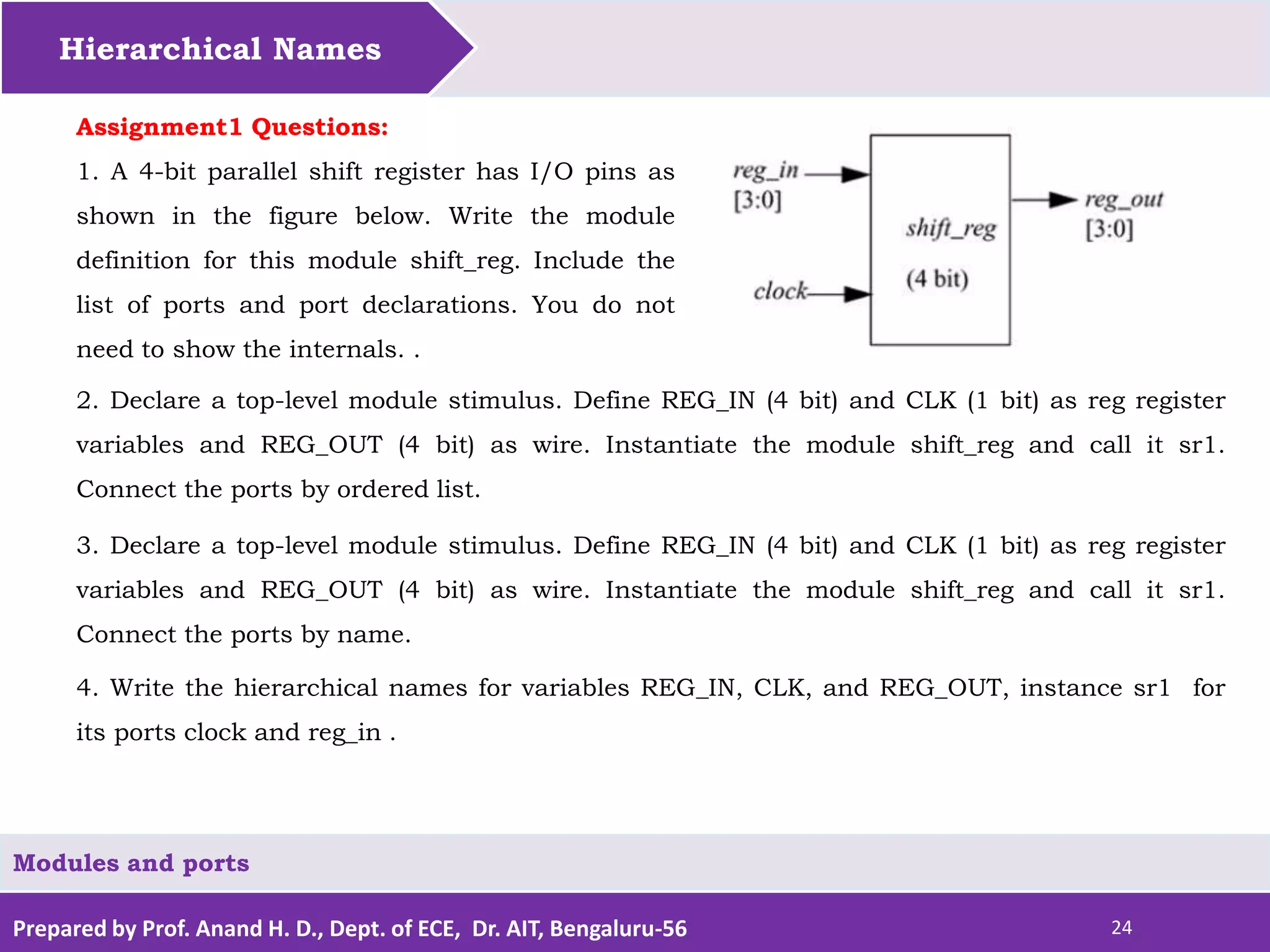


The document discusses modules and ports in Verilog. It describes that a module defines distinct parts including module name, port list, port declarations, and optional parameters. Ports provide the interface for a module to communicate with its environment. There are two methods for connecting ports to external signals - by ordered list where signals must appear in the same order as ports, and by name where the order does not matter as long as port names match. Hierarchical names provide unique names for every identifier by denoting the design hierarchy with identifiers separated by periods.