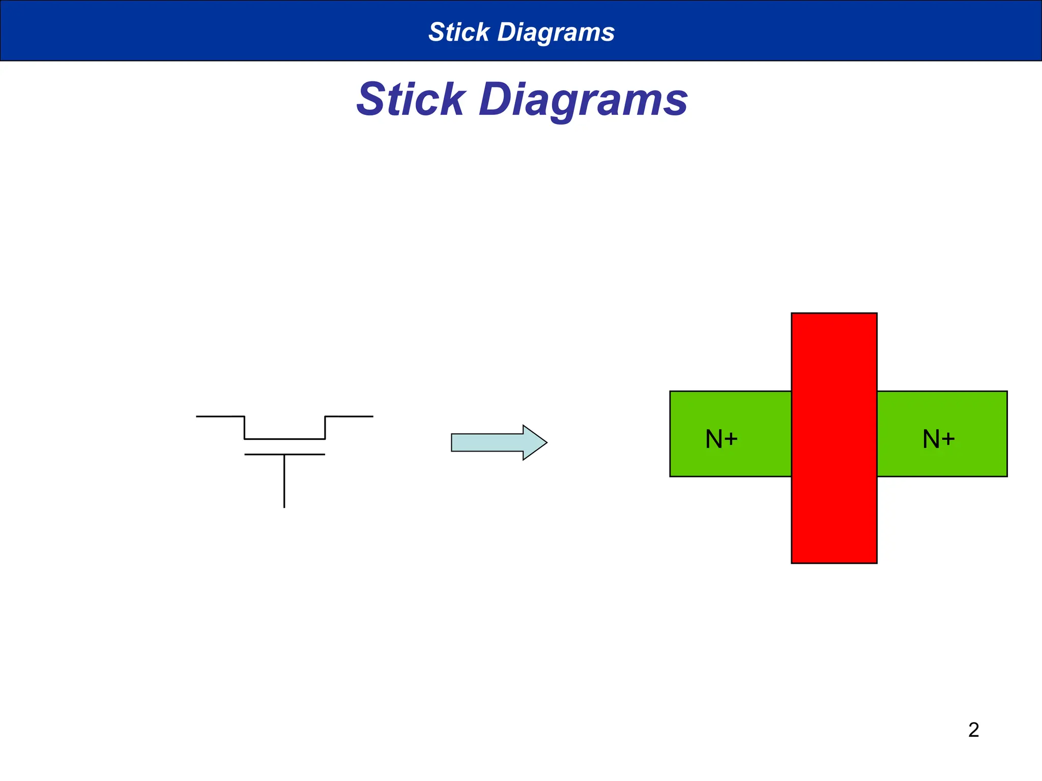
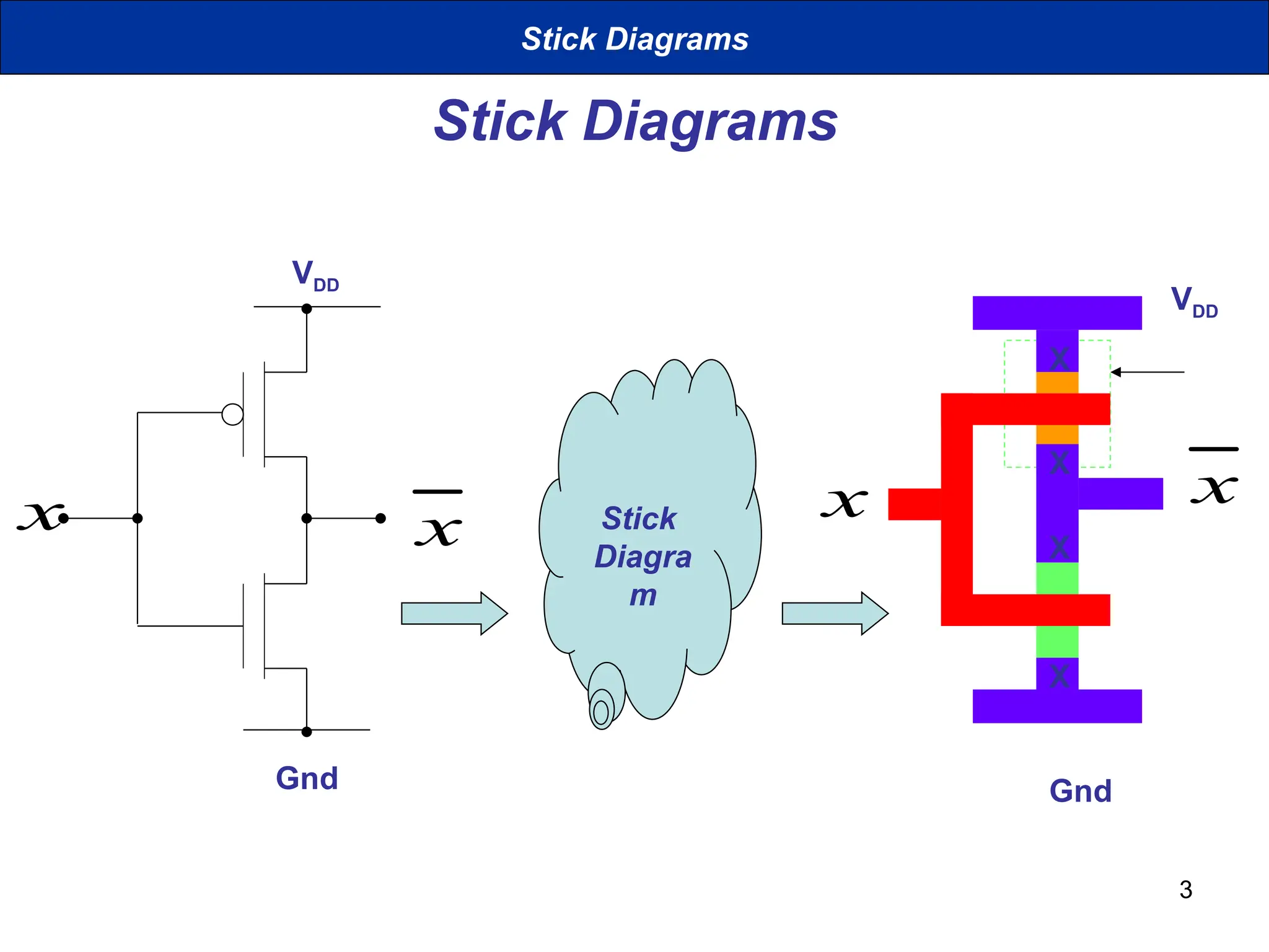
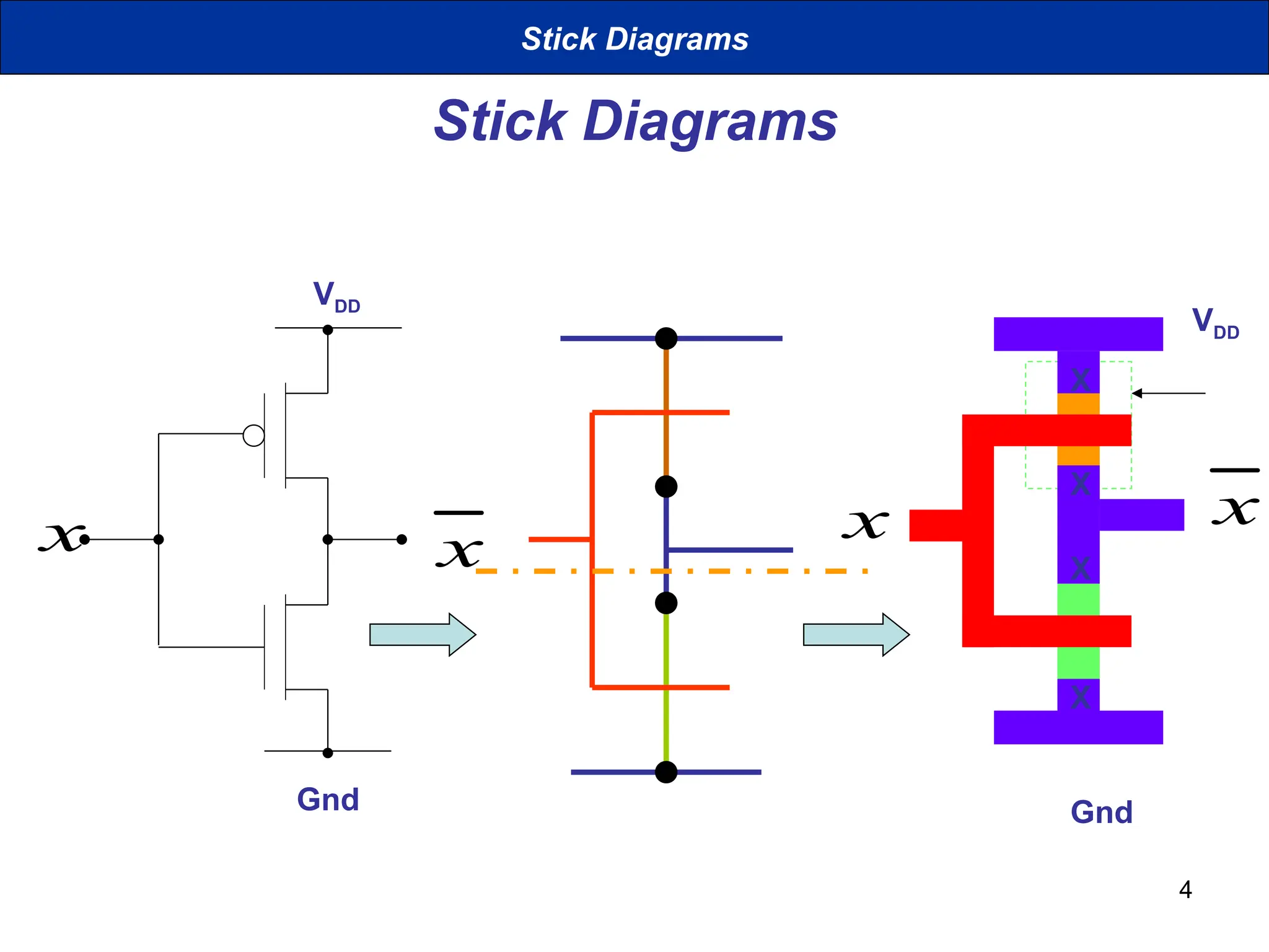
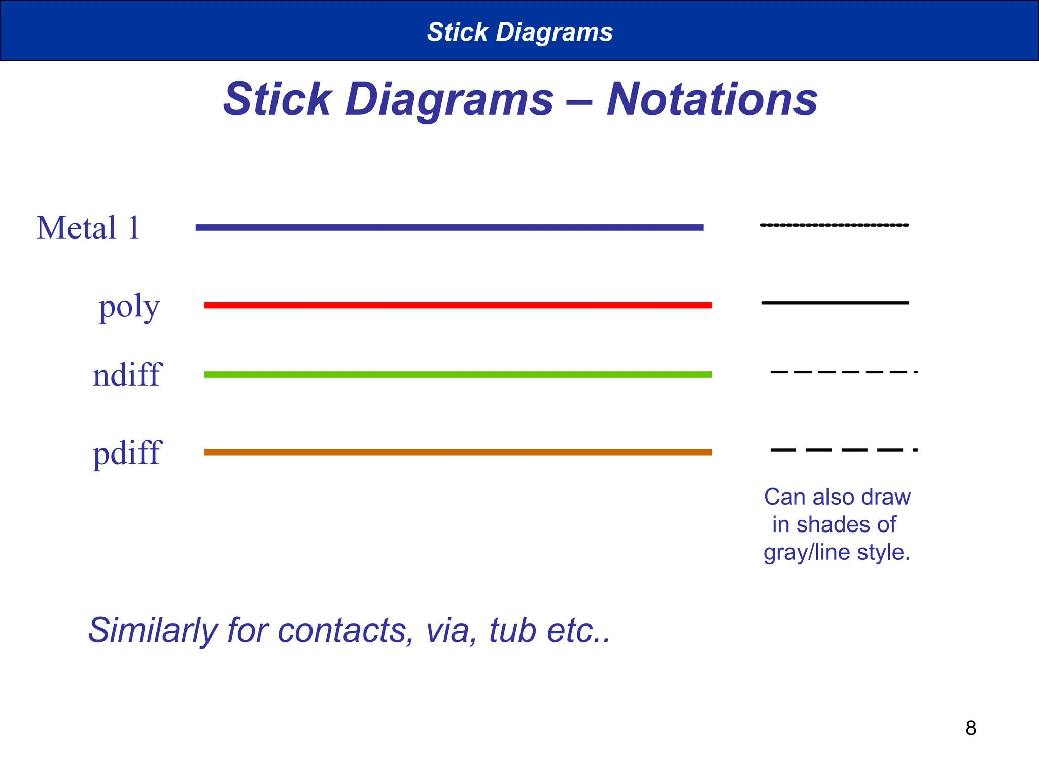
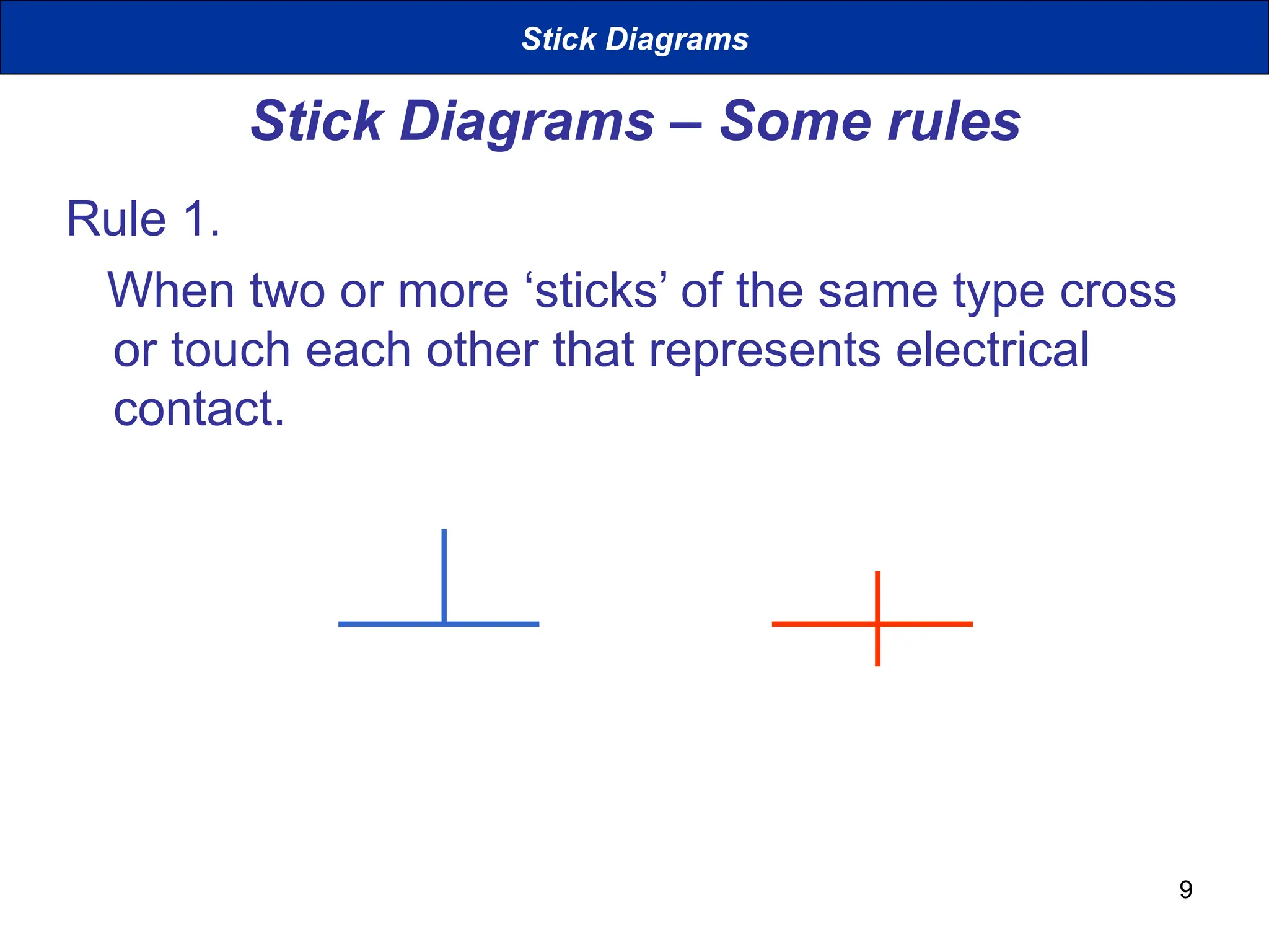
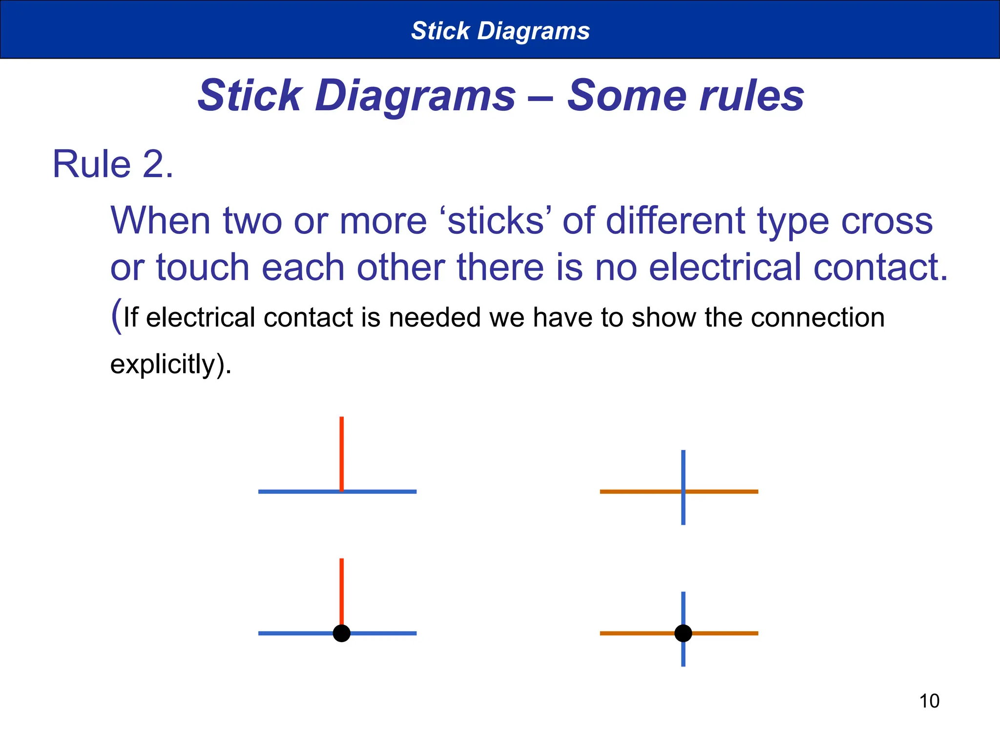
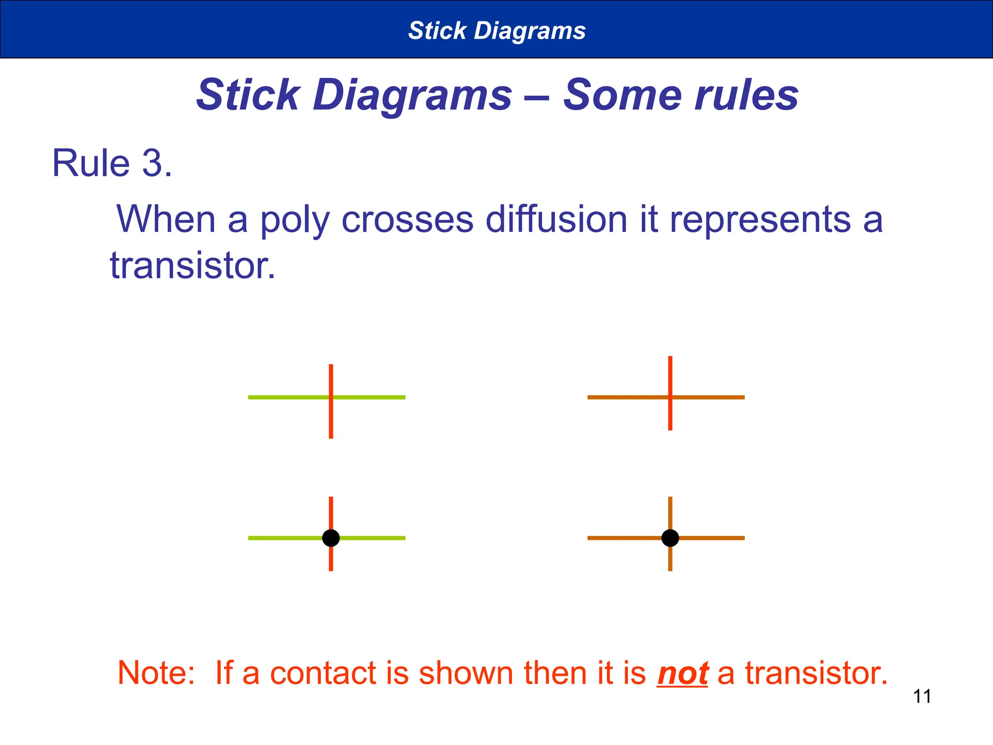
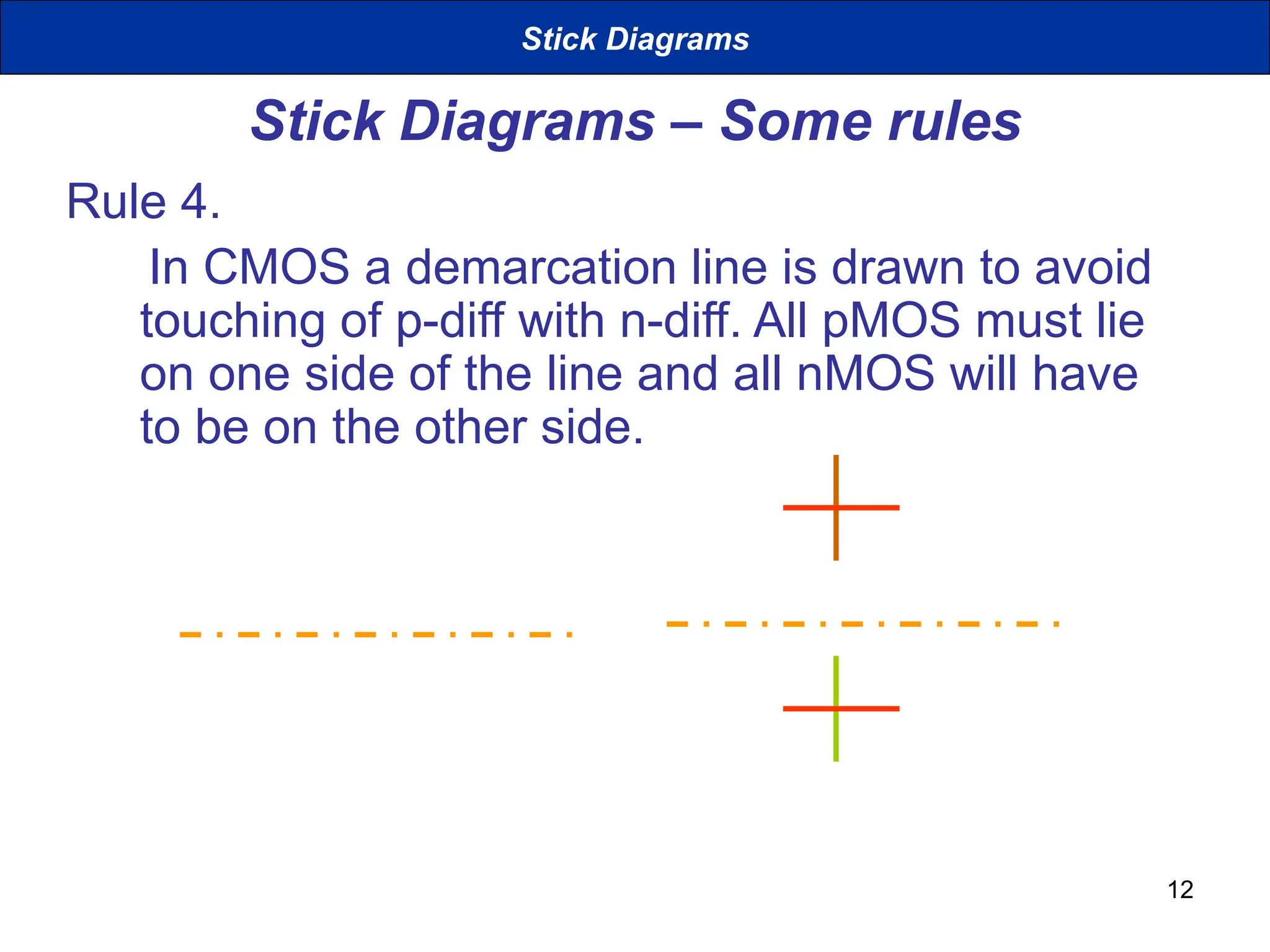
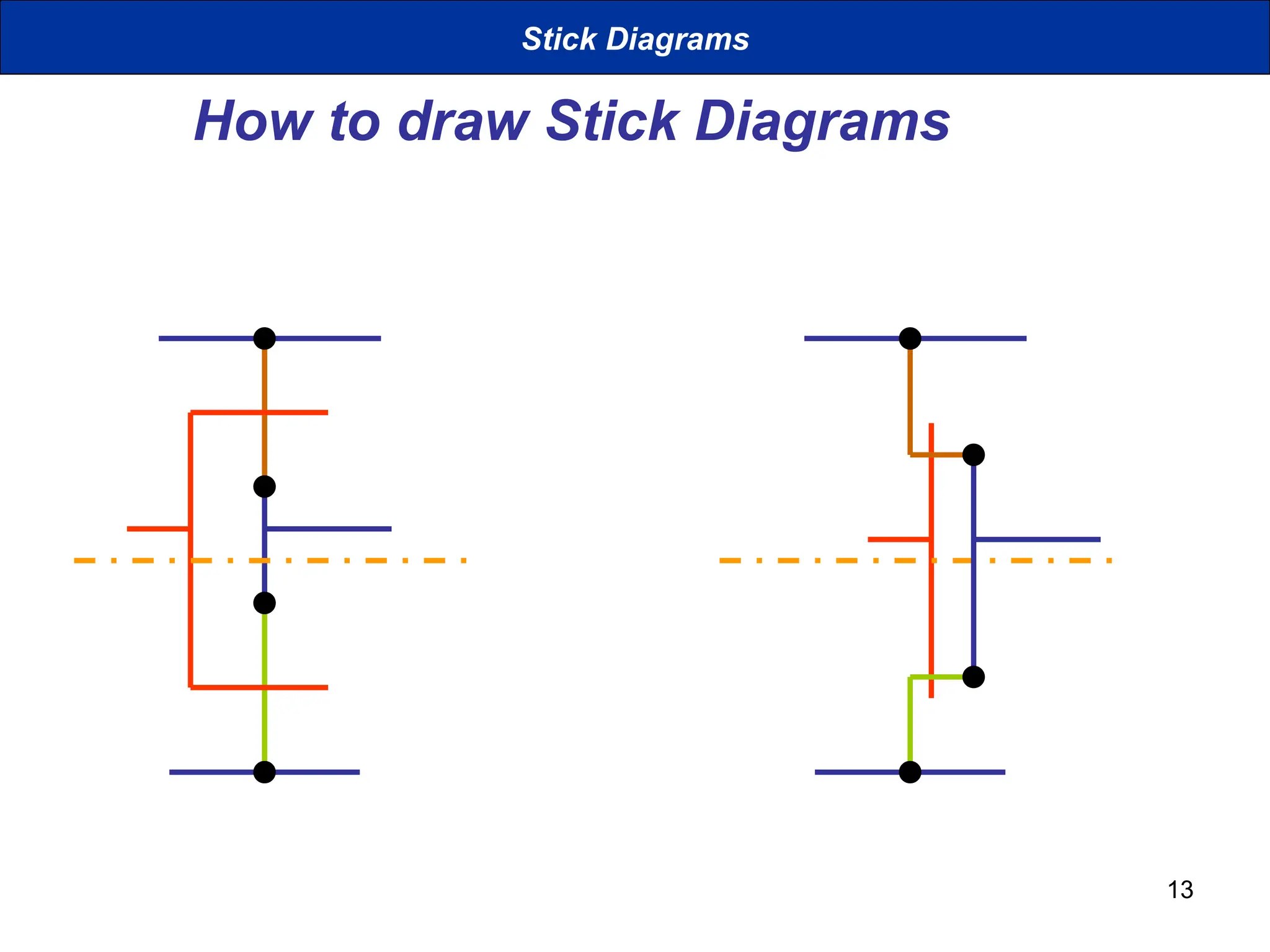
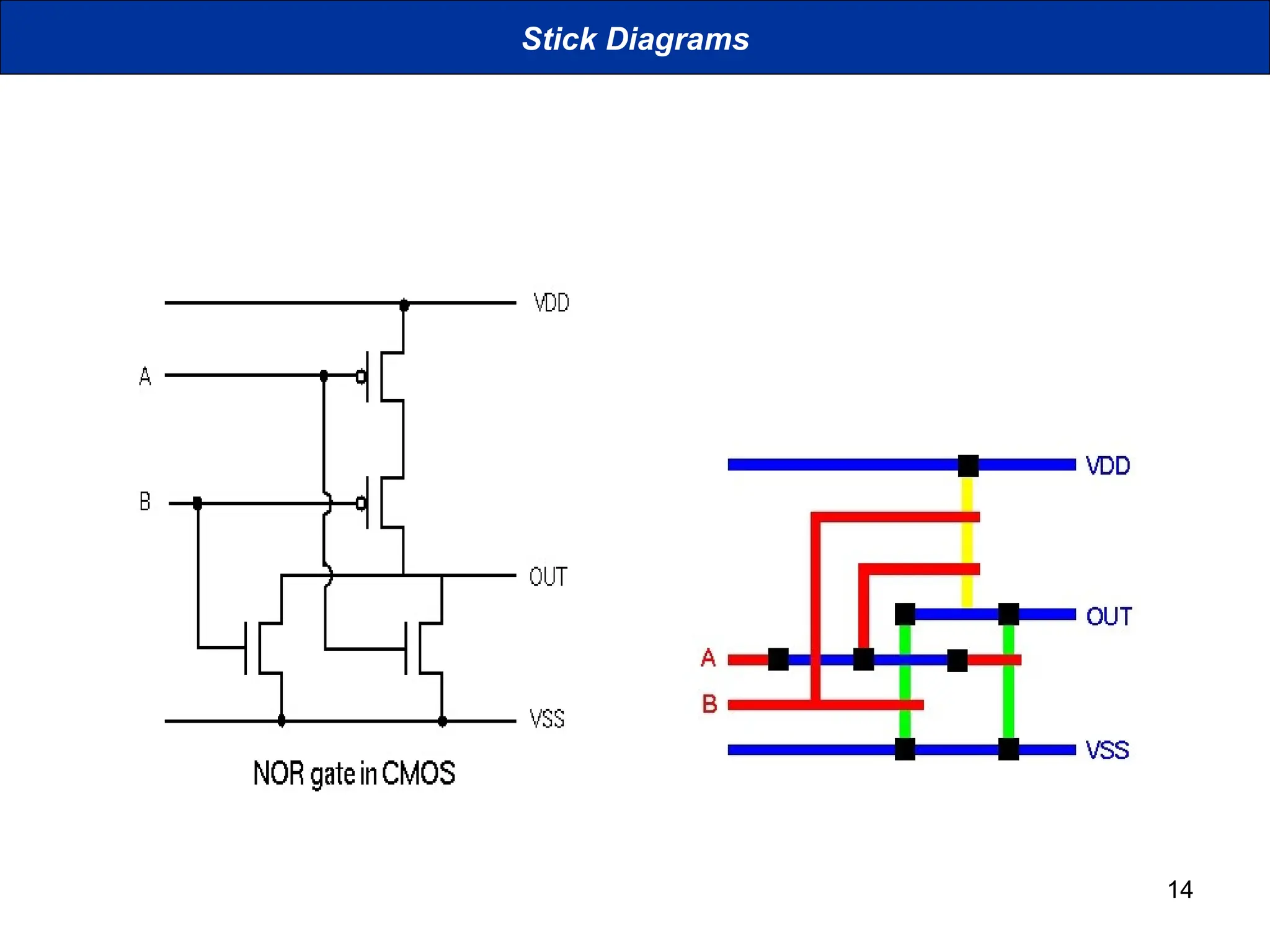
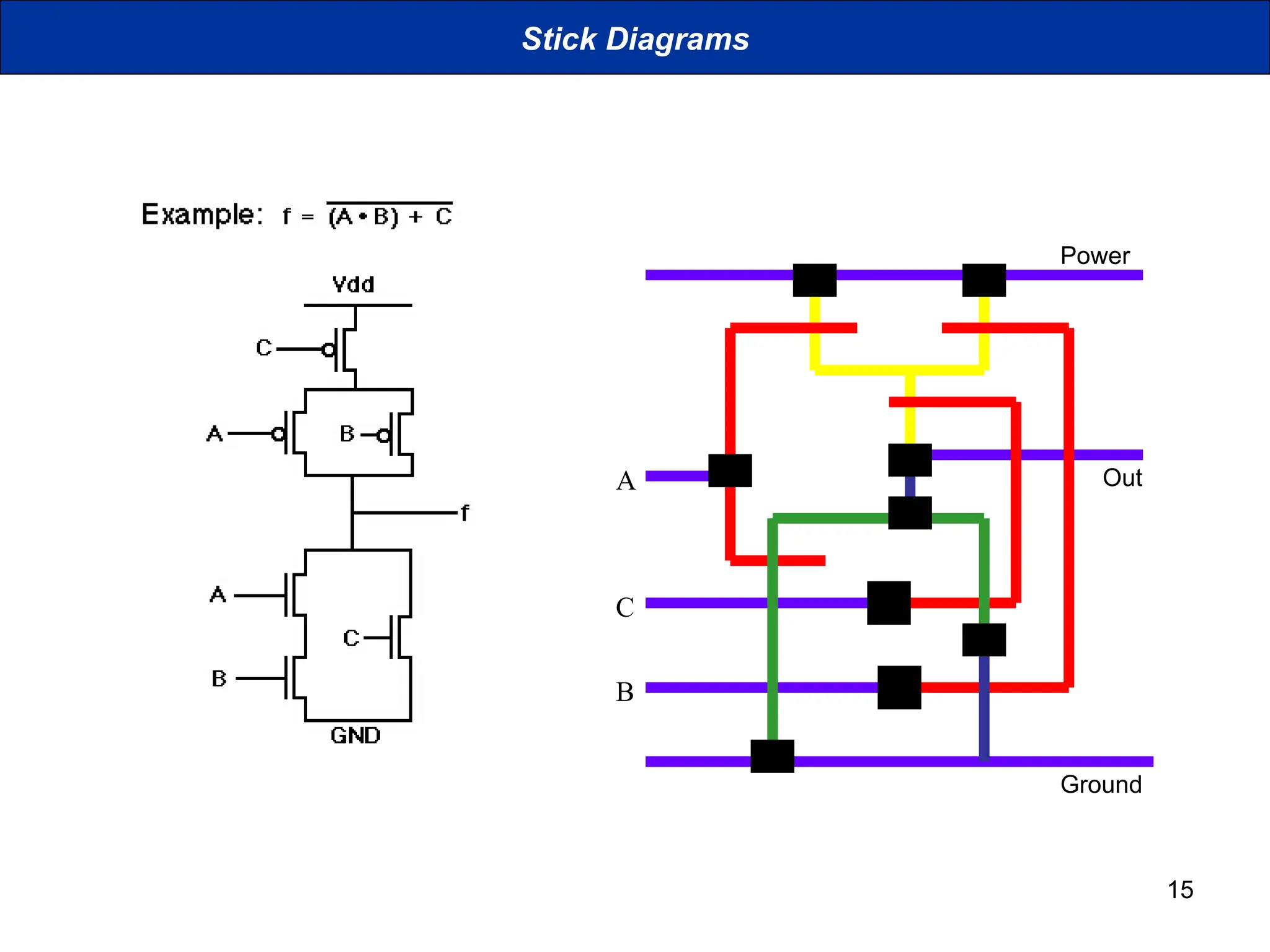
1
Stick Diagrams
Stick Diagrams
2
Stick Diagrams
N+ N+
Stick Diagrams
3
Stick Diagrams
Gnd
VDD
x x
X
X
X
X
VDD
x x
Gnd
Stick
Diagra
m
Stick Diagrams
4
Stick Diagrams
Gnd
VDD
x x
X
X
X
X
VDD
x x
Gnd
Stick Diagrams
5
Stick Diagrams
 VLSI design aims to translate circuit concepts
onto silicon.
 stick diagrams are a means of capturing
topography and layer information using
simple diagrams.
 Stick diagrams convey layer information
through colour codes (or monochrome
encoding).
 Acts as an interface between symbolic circuit
and the actual layout.
6
Stick Diagrams
 Does show all components/vias.
 It shows relative placement of components.
 Goes one step closer to the layout
 Helps plan the layout and routing
A stick diagram is a cartoon of a layout.
Stick Diagrams
S.N.Bhat, Faculty, Dept. of E&C Engineering, M.I.T Manipal
7
Stick Diagrams
 Does not show
• Exact placement of components
• Transistor sizes
• Wire lengths, wire widths, tub boundaries.
• Any other low level details such as parasitics..
Stick Diagrams
8
Stick Diagrams – Notations
Metal 1
poly
ndiff
pdiff
Can also draw
in shades of
gray/line style.
Stick Diagrams
Similarly for contacts, via, tub etc..
9
Stick Diagrams – Some rules
Rule 1.
When two or more ‘sticks’ of the same type cross
or touch each other that represents electrical
contact.
Stick Diagrams
10
Stick Diagrams – Some rules
Rule 2.
When two or more ‘sticks’ of different type cross
or touch each other there is no electrical contact.
(If electrical contact is needed we have to show the connection
explicitly).
Stick Diagrams
11
Stick Diagrams – Some rules
Rule 3.
When a poly crosses diffusion it represents a
transistor.
Note: If a contact is shown then it is not a transistor.
Stick Diagrams
12
Stick Diagrams – Some rules
Rule 4.
In CMOS a demarcation line is drawn to avoid
touching of p-diff with n-diff. All pMOS must lie
on one side of the line and all nMOS will have
to be on the other side.
Stick Diagrams
13
How to draw Stick Diagrams
Stick Diagrams
14
Stick Diagrams
15
Power
Ground
B
C
Out
A
Stick Diagrams
16
Stick Diagrams
1. Draw the stick diagram for two input CMOS NAND
gate.
2. Draw the stick diagram for two input NAND gate
using NMOS Logic.
3. Draw the stick diagram for 2:1 MUX using
a) Pass transistors
b) Transmission gates.
Stick Diagrams

stick diagrams is a cartton of layout which helps in designing and synthesis of circuits

  • 1.
  • 2.
  • 3.
    3 Stick Diagrams Gnd VDD x x X X X X VDD xx Gnd Stick Diagra m Stick Diagrams
  • 4.
  • 5.
    5 Stick Diagrams  VLSIdesign aims to translate circuit concepts onto silicon.  stick diagrams are a means of capturing topography and layer information using simple diagrams.  Stick diagrams convey layer information through colour codes (or monochrome encoding).  Acts as an interface between symbolic circuit and the actual layout.
  • 6.
    6 Stick Diagrams  Doesshow all components/vias.  It shows relative placement of components.  Goes one step closer to the layout  Helps plan the layout and routing A stick diagram is a cartoon of a layout. Stick Diagrams S.N.Bhat, Faculty, Dept. of E&C Engineering, M.I.T Manipal
  • 7.
    7 Stick Diagrams  Doesnot show • Exact placement of components • Transistor sizes • Wire lengths, wire widths, tub boundaries. • Any other low level details such as parasitics.. Stick Diagrams
  • 8.
    8 Stick Diagrams –Notations Metal 1 poly ndiff pdiff Can also draw in shades of gray/line style. Stick Diagrams Similarly for contacts, via, tub etc..
  • 9.
    9 Stick Diagrams –Some rules Rule 1. When two or more ‘sticks’ of the same type cross or touch each other that represents electrical contact. Stick Diagrams
  • 10.
    10 Stick Diagrams –Some rules Rule 2. When two or more ‘sticks’ of different type cross or touch each other there is no electrical contact. (If electrical contact is needed we have to show the connection explicitly). Stick Diagrams
  • 11.
    11 Stick Diagrams –Some rules Rule 3. When a poly crosses diffusion it represents a transistor. Note: If a contact is shown then it is not a transistor. Stick Diagrams
  • 12.
    12 Stick Diagrams –Some rules Rule 4. In CMOS a demarcation line is drawn to avoid touching of p-diff with n-diff. All pMOS must lie on one side of the line and all nMOS will have to be on the other side. Stick Diagrams
  • 13.
    13 How to drawStick Diagrams Stick Diagrams
  • 14.
  • 15.
  • 16.
    16 Stick Diagrams 1. Drawthe stick diagram for two input CMOS NAND gate. 2. Draw the stick diagram for two input NAND gate using NMOS Logic. 3. Draw the stick diagram for 2:1 MUX using a) Pass transistors b) Transmission gates. Stick Diagrams