Download to read offline
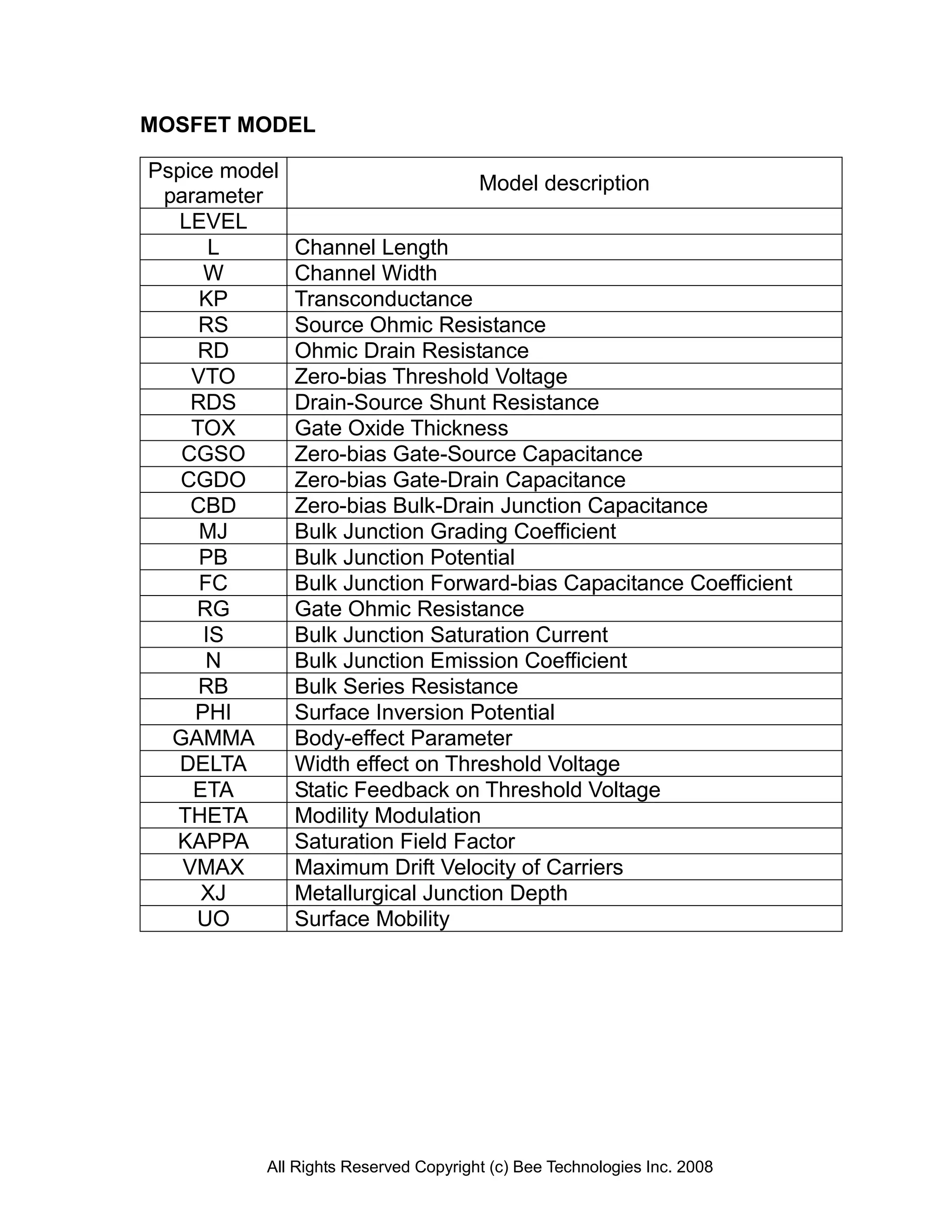
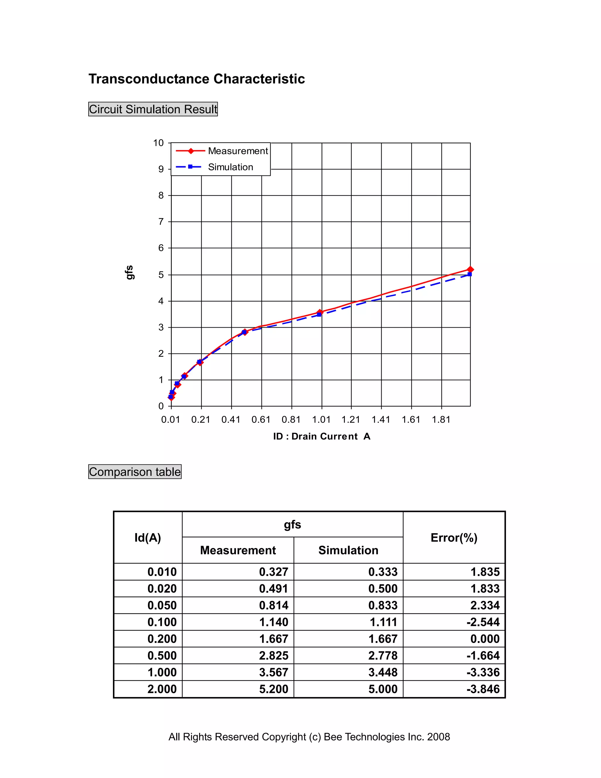
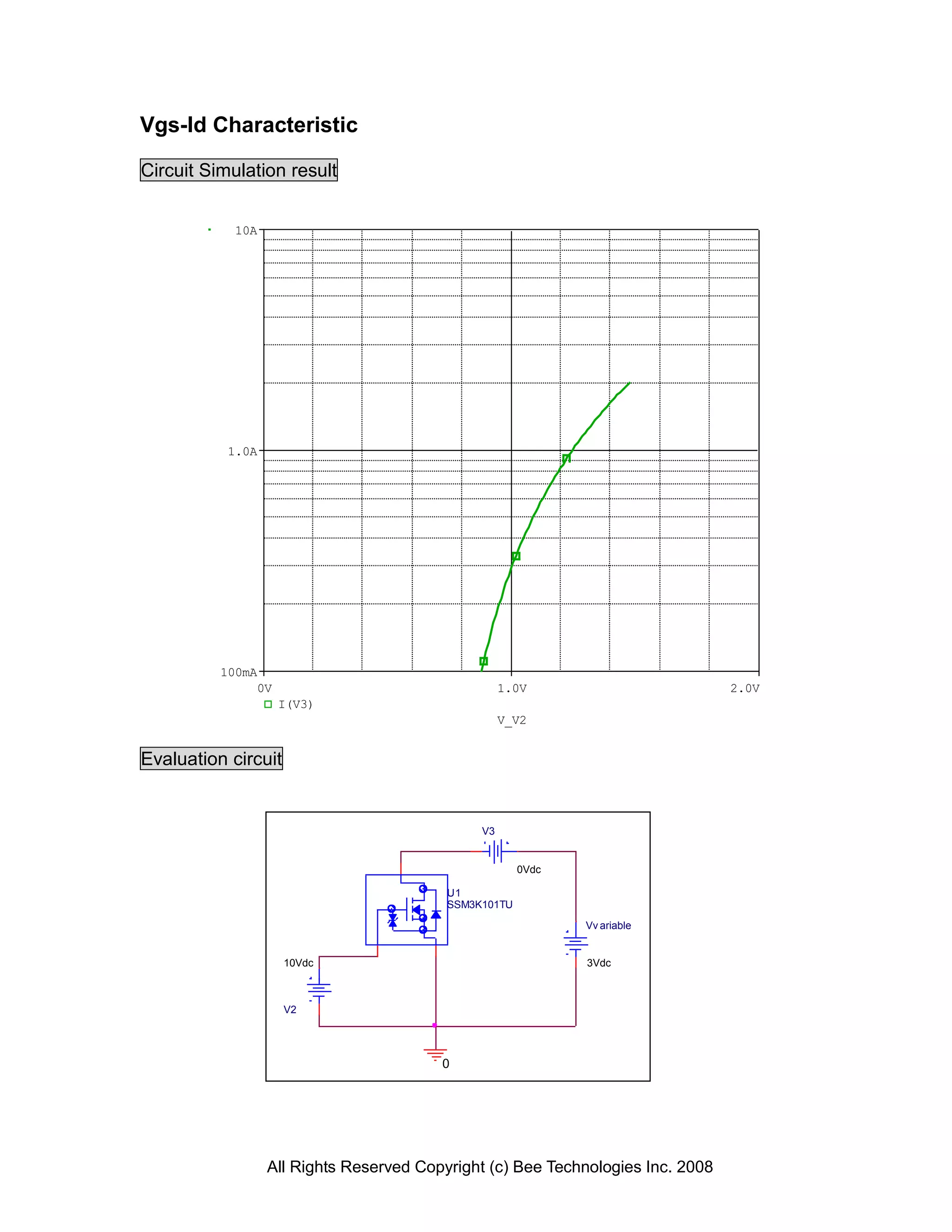
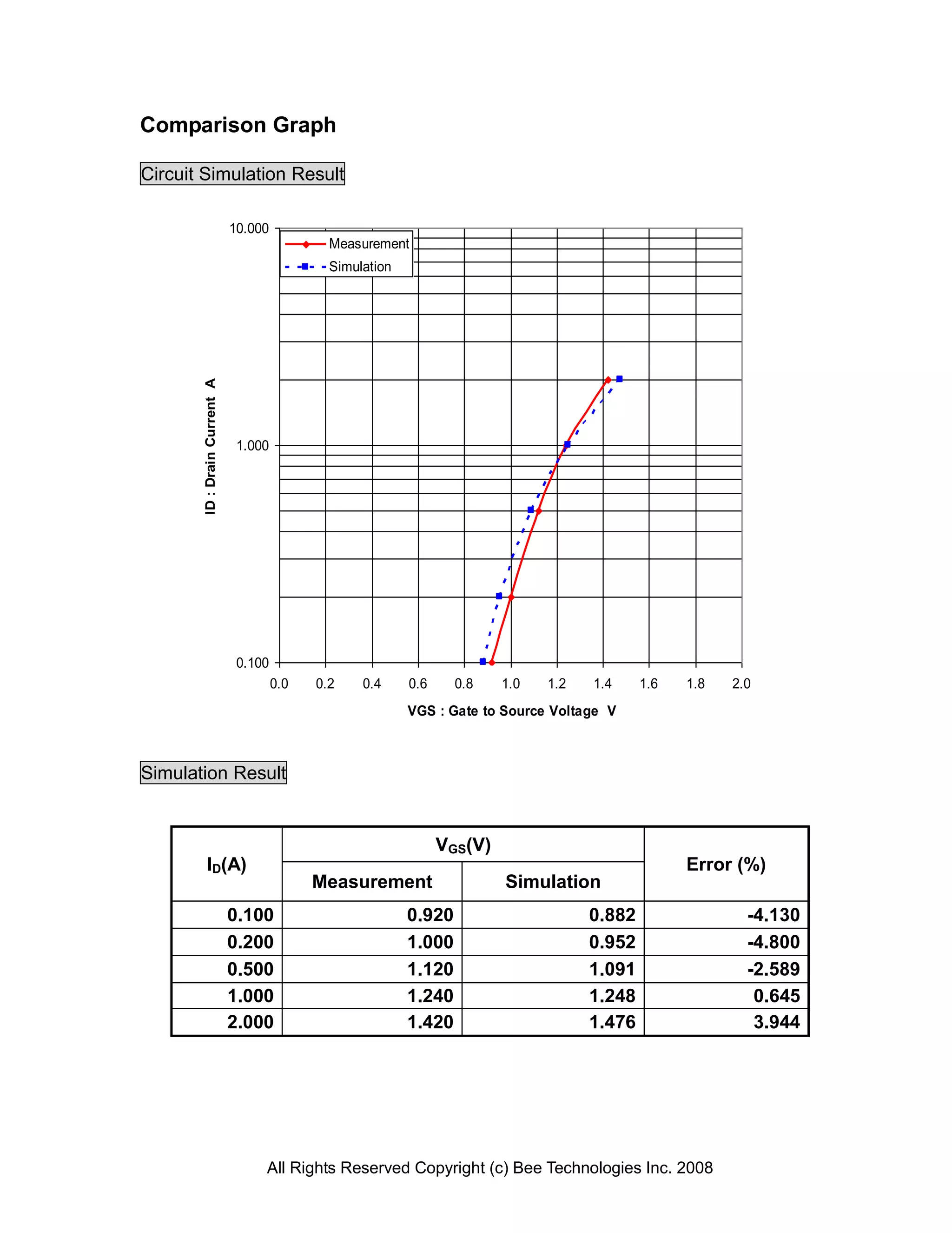
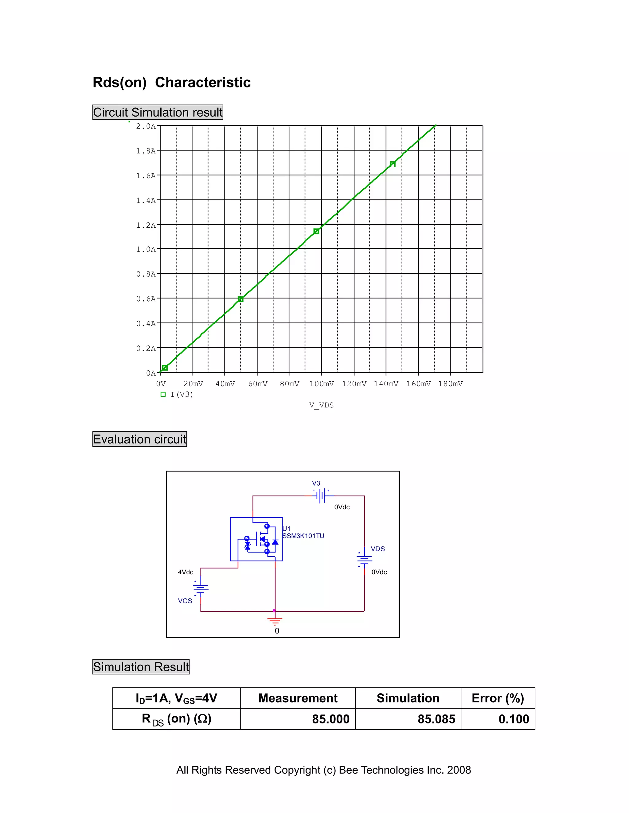
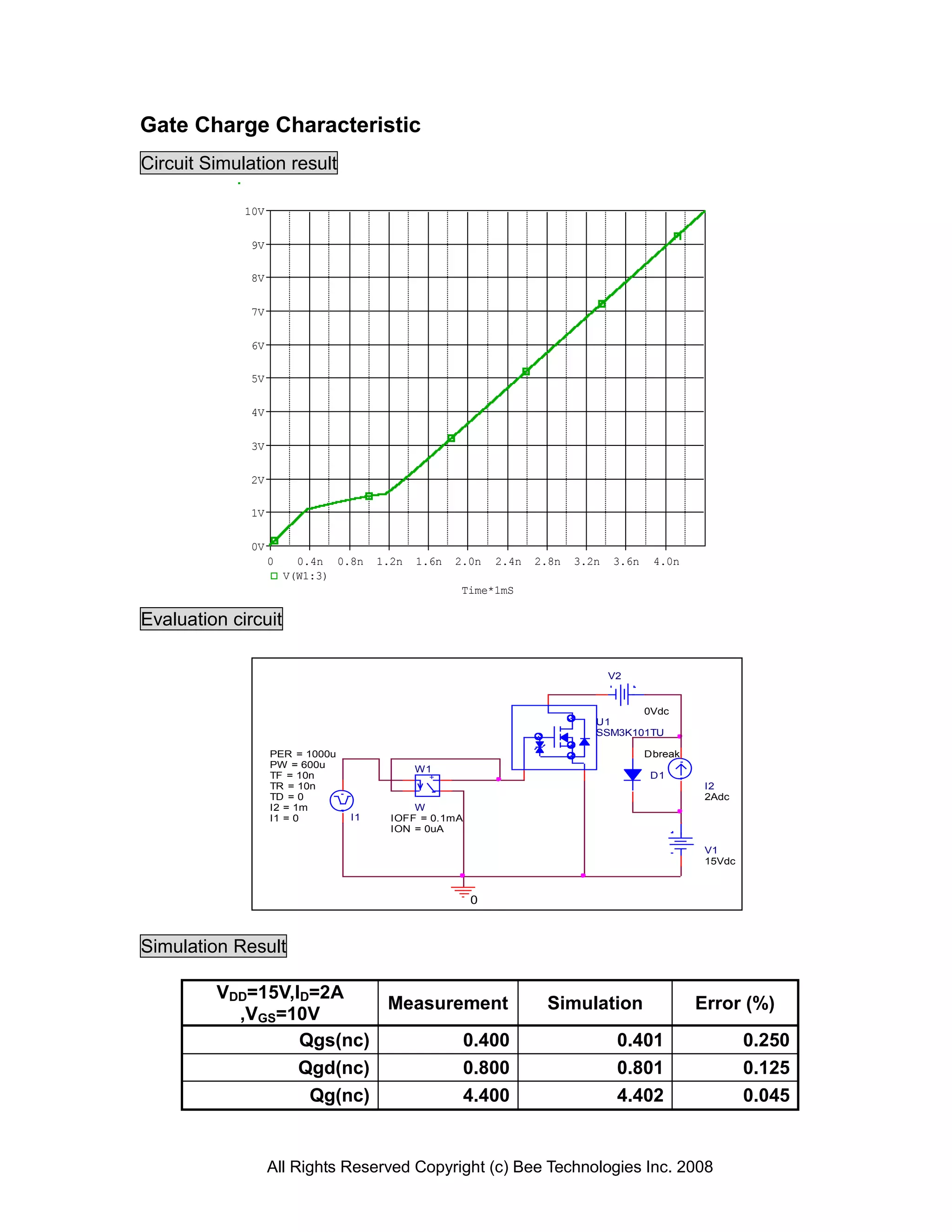

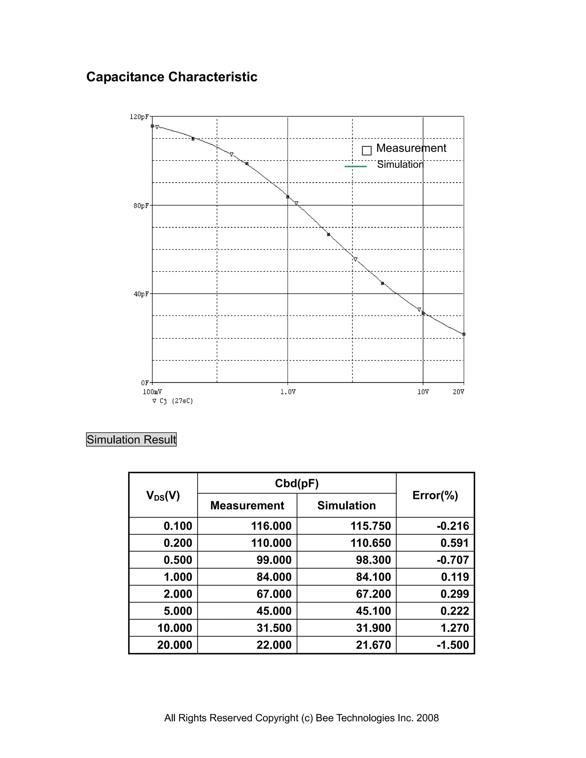
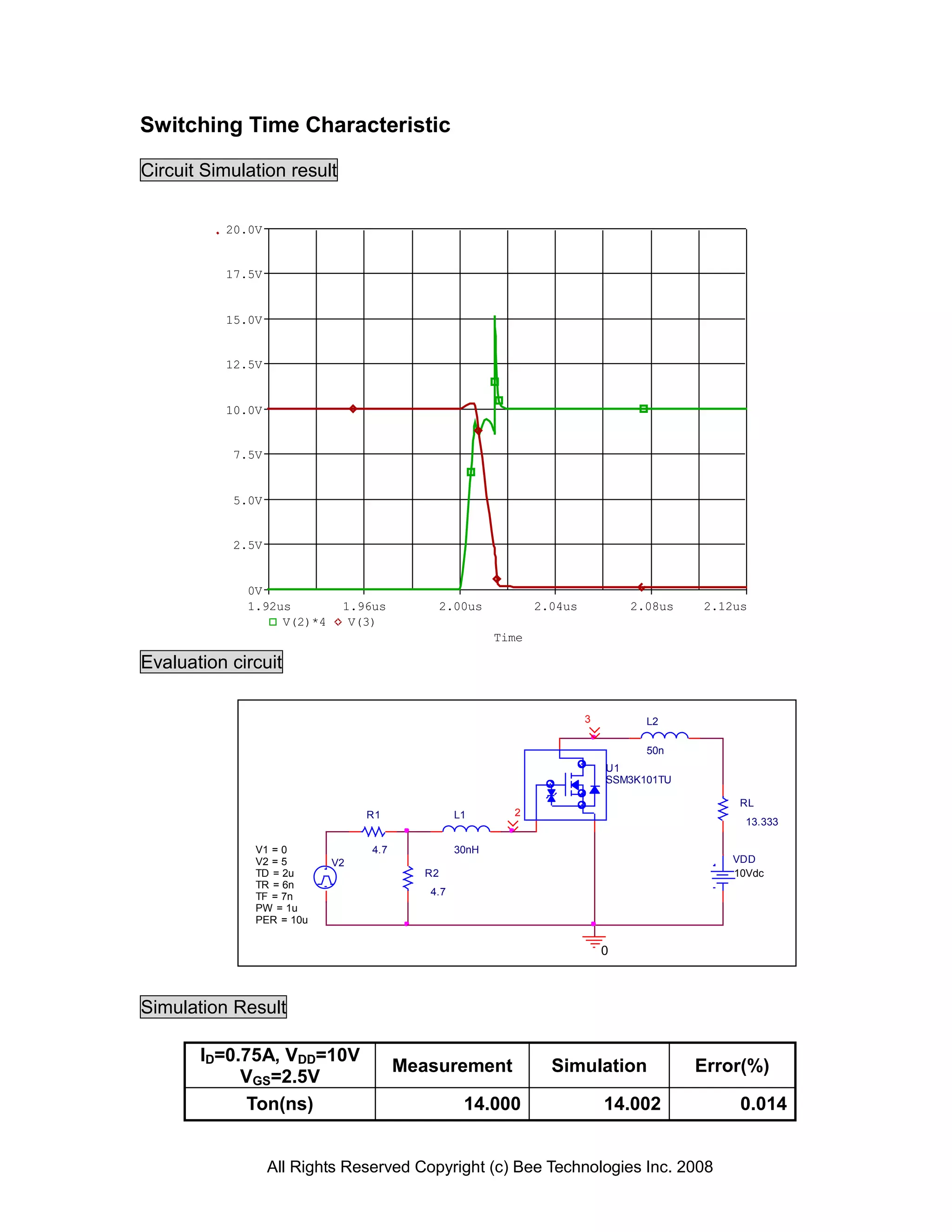
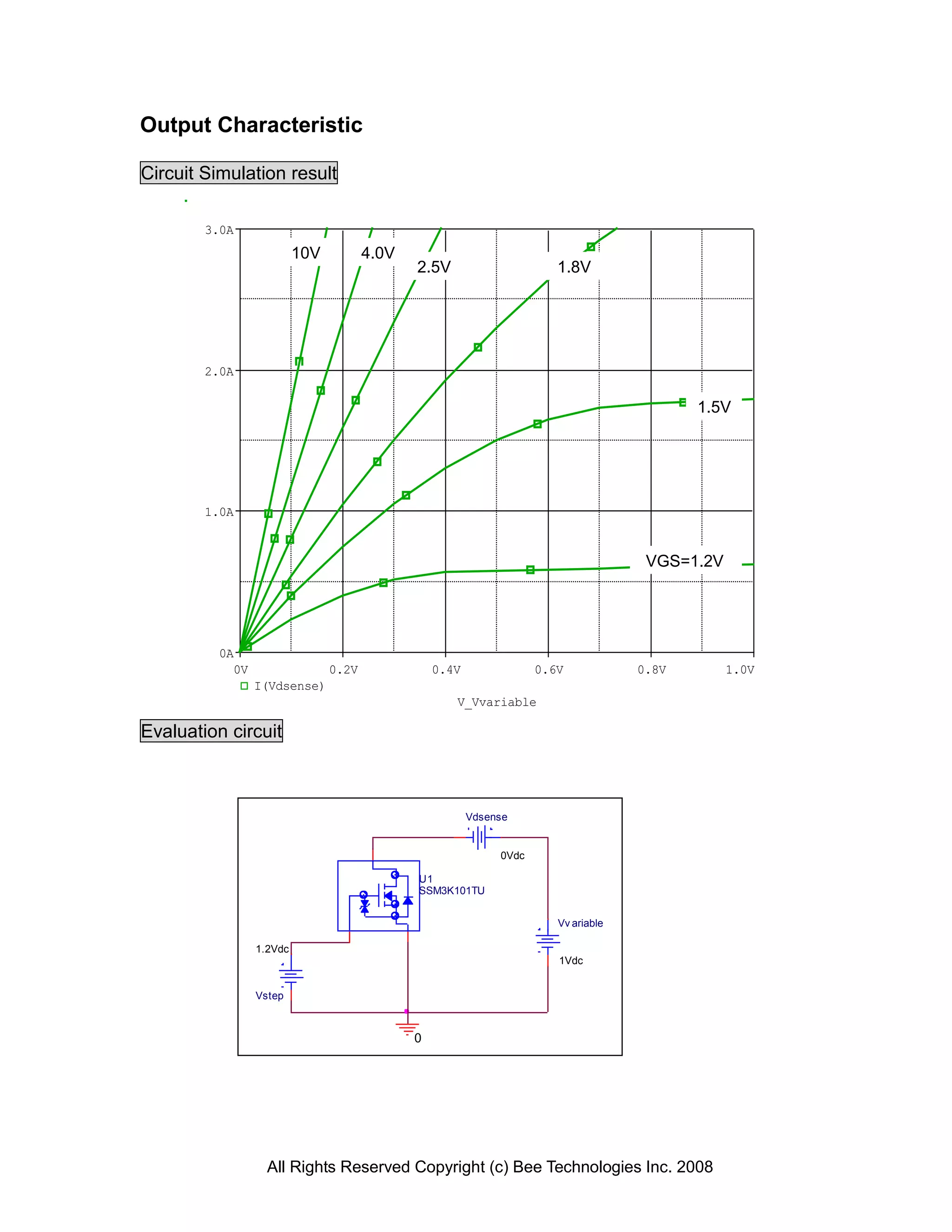
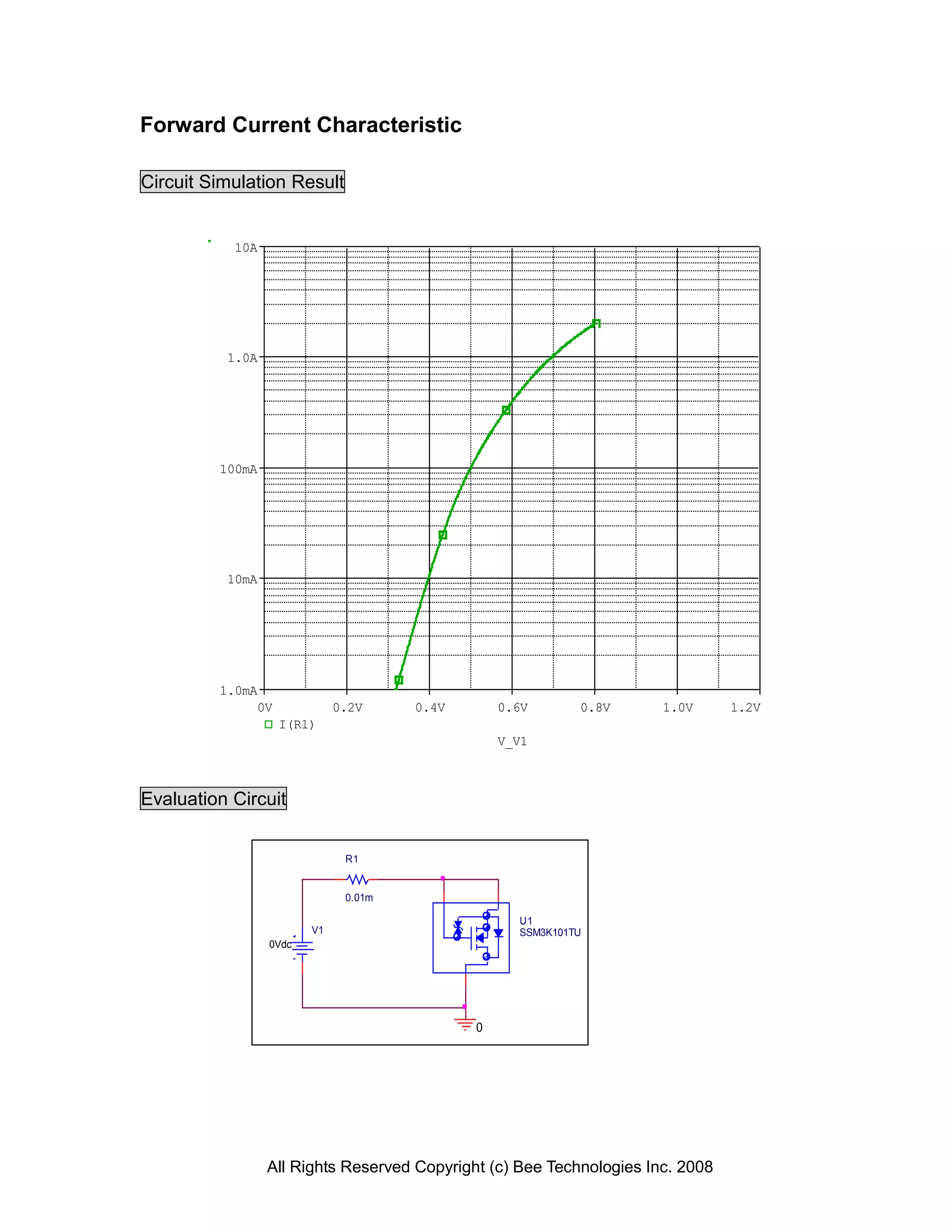
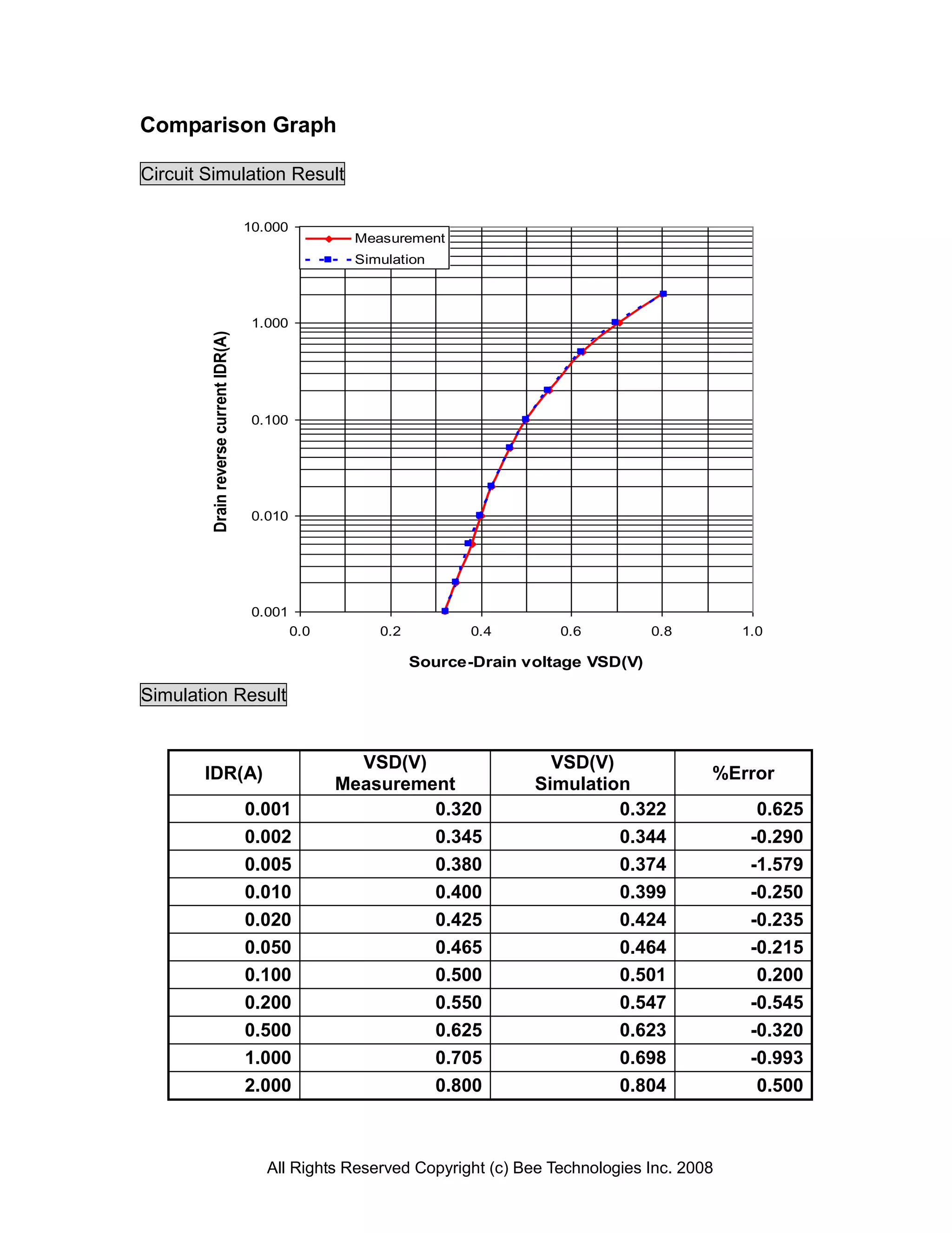
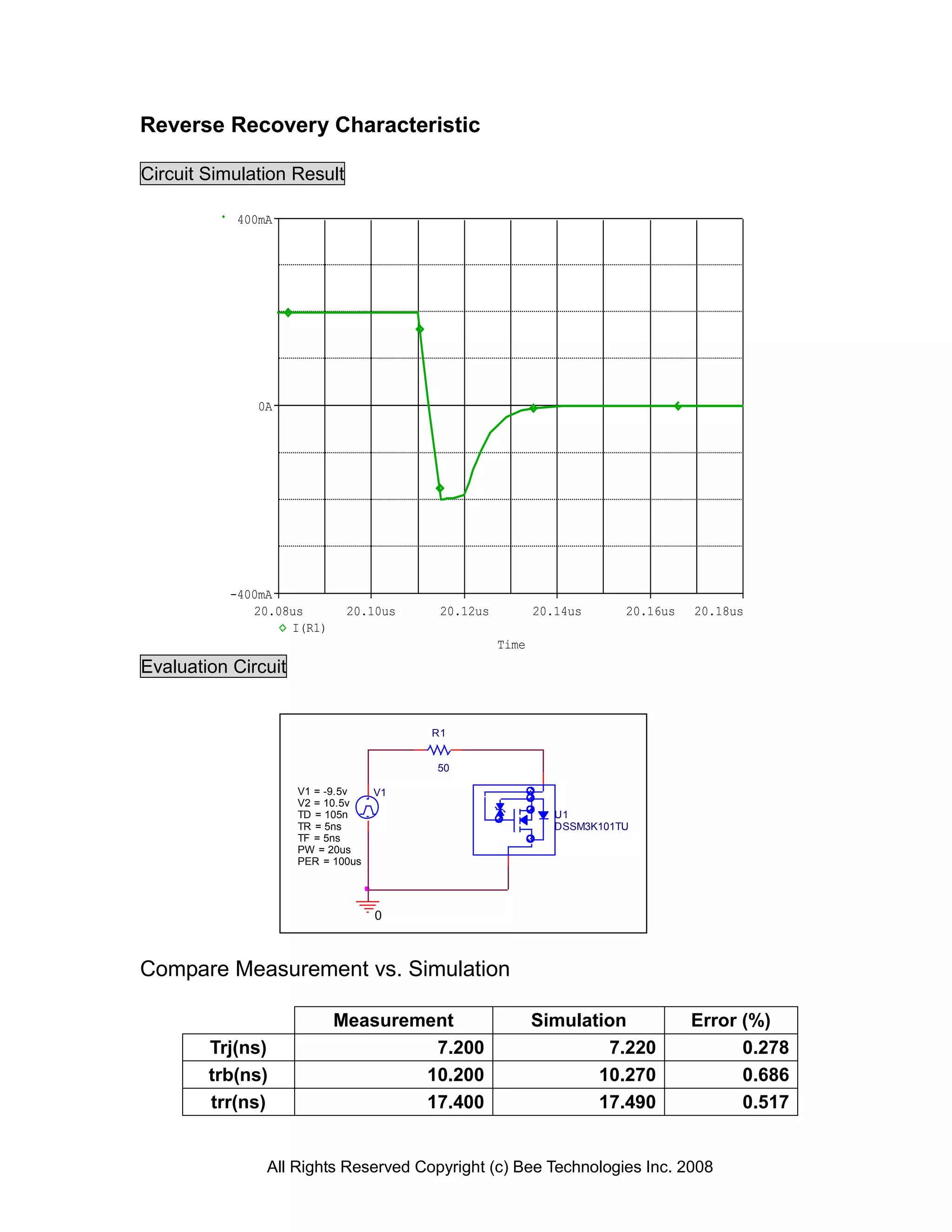
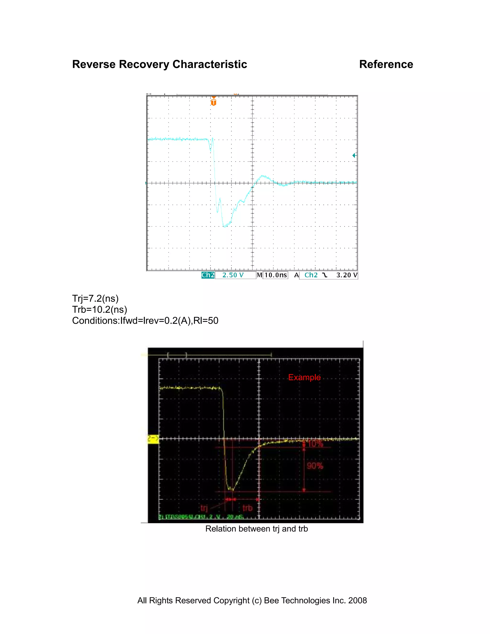
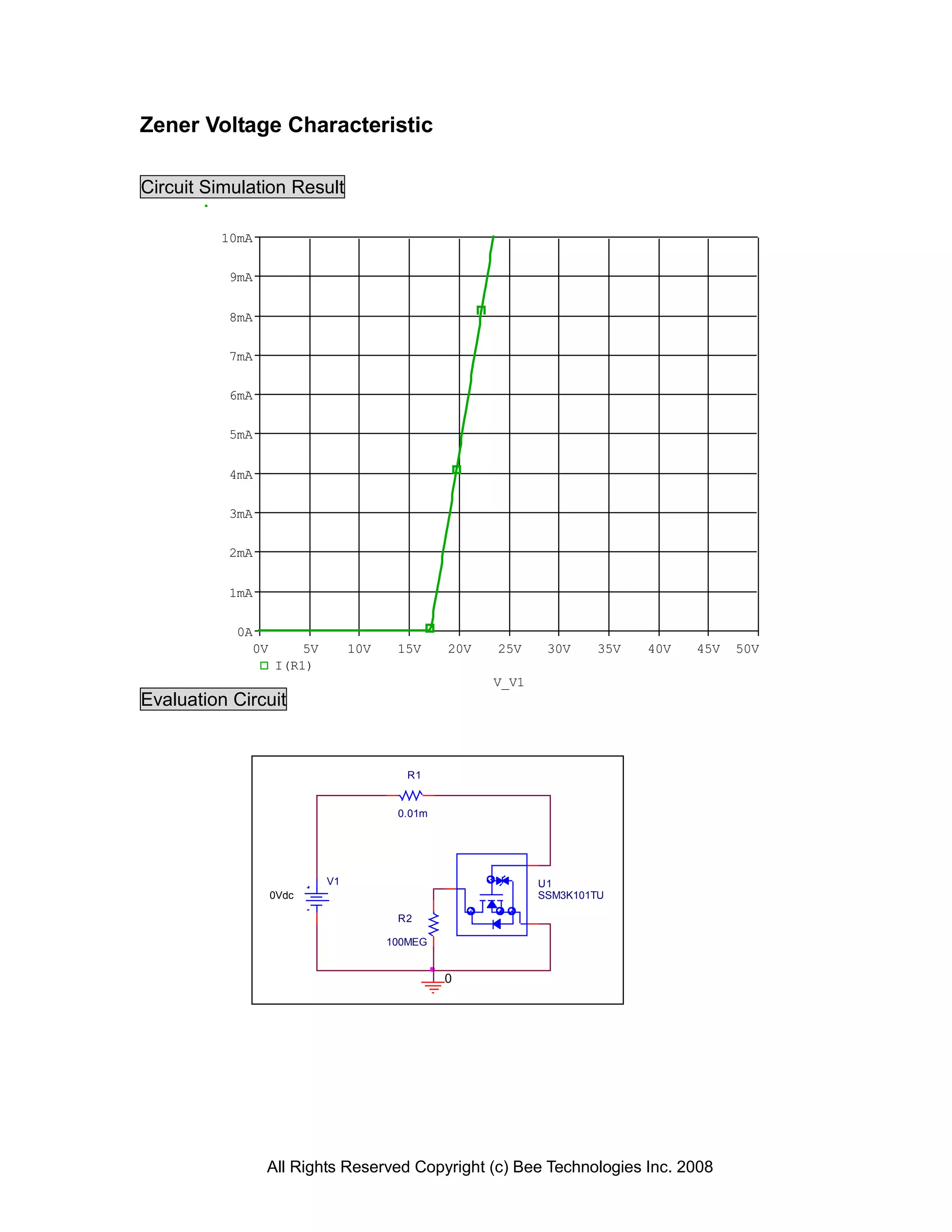
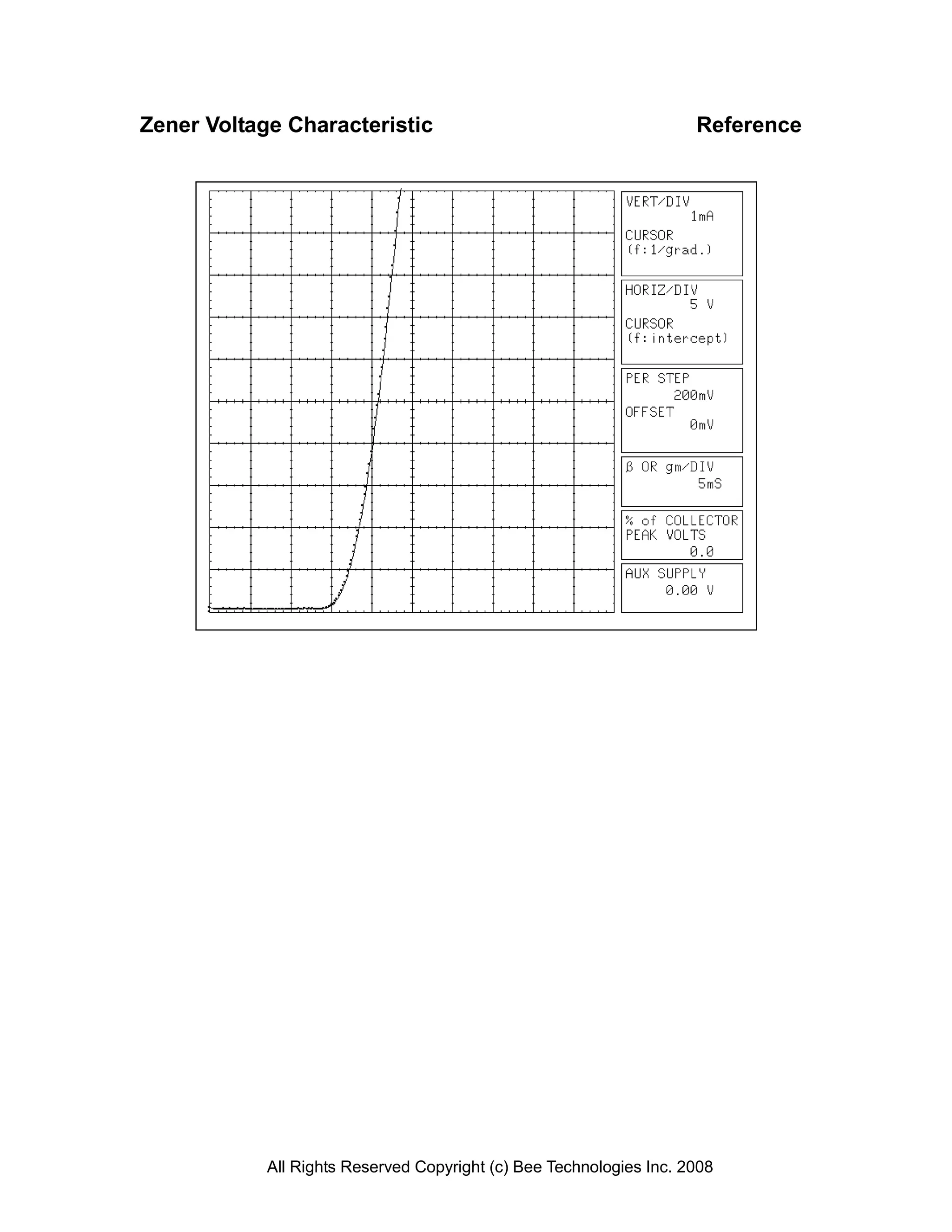

The document provides a detailed device modeling report for the SSM3K101TU power MOSFET, including characteristics such as transconductance, gate charge, and switching time. It contains simulation results, comparison tables between measurements and simulations, and various circuit simulation results highlighting the device's performance and behavior under specific conditions. All data, including voltage and current characteristics, is thoroughly presented to analyze the performance accuracy of the MOSFET model.


