Download to read offline
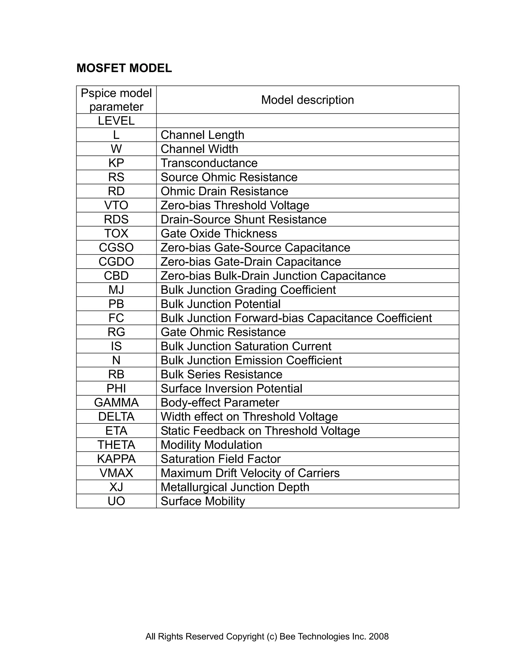
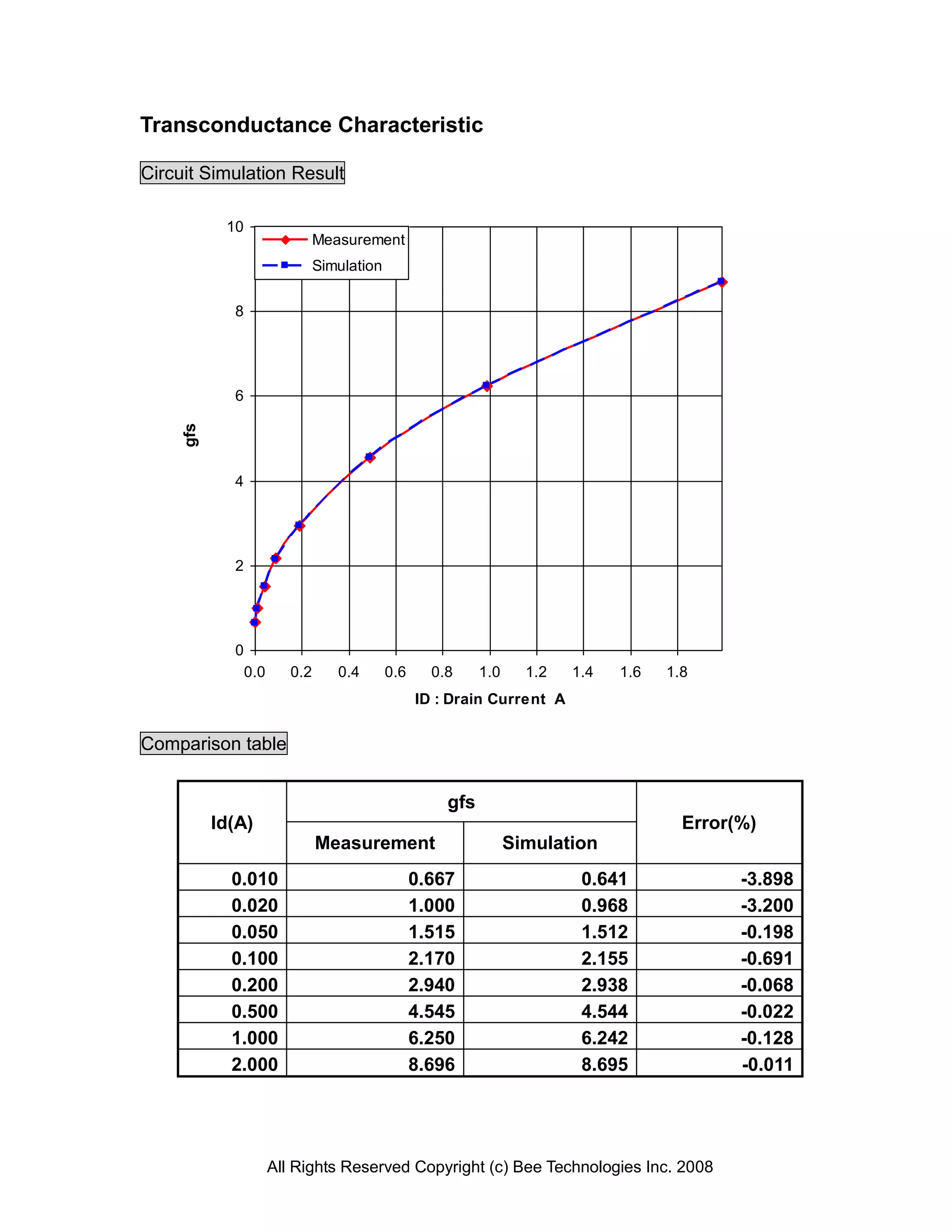
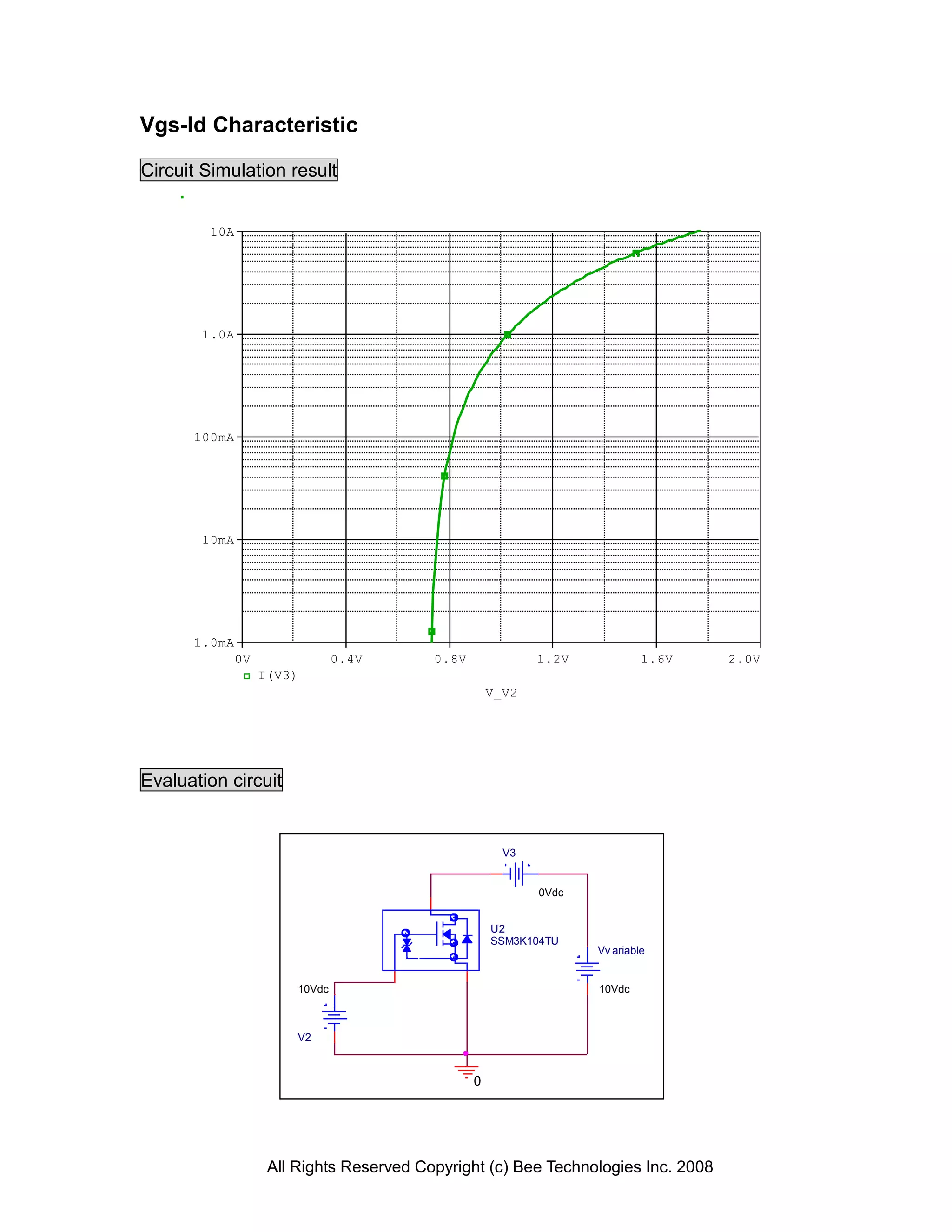
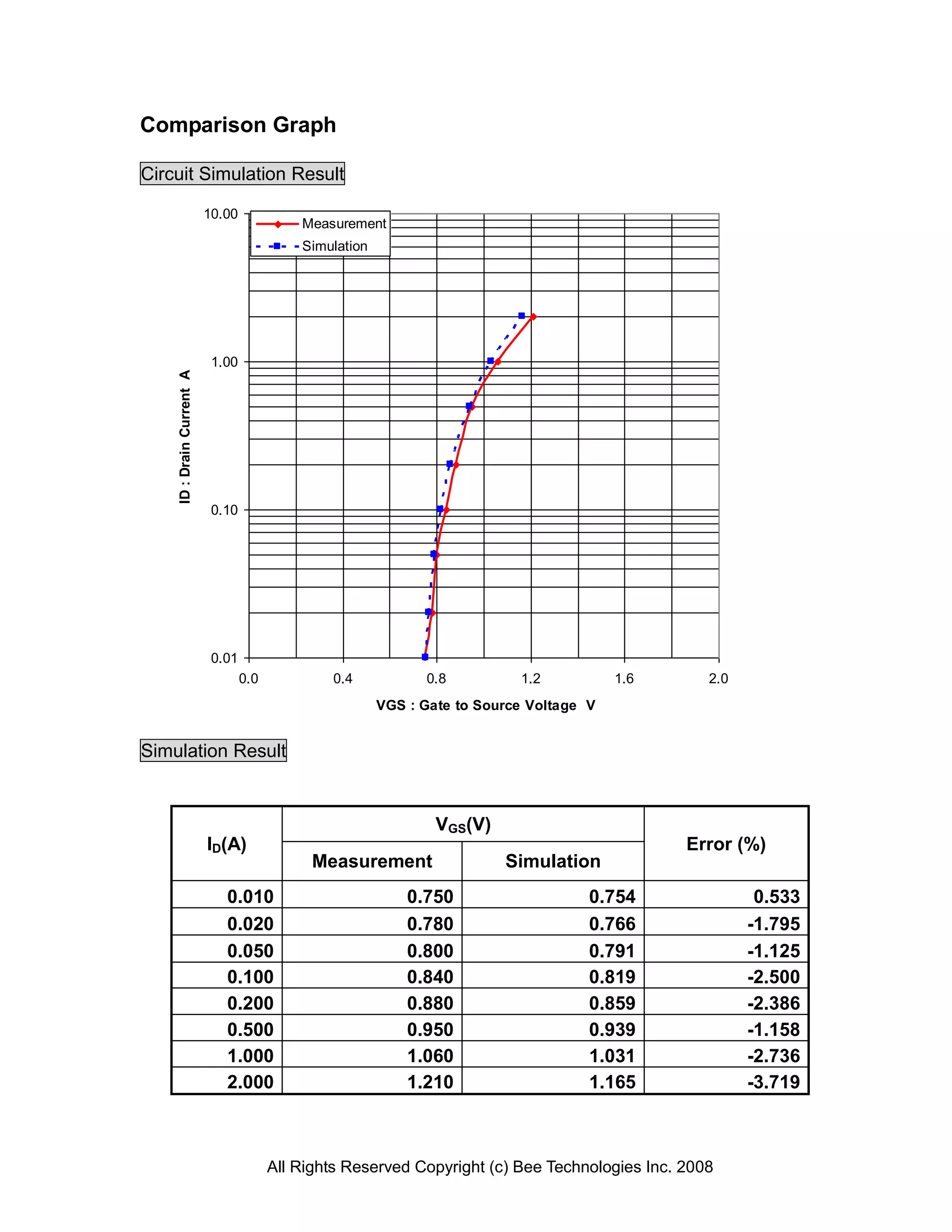
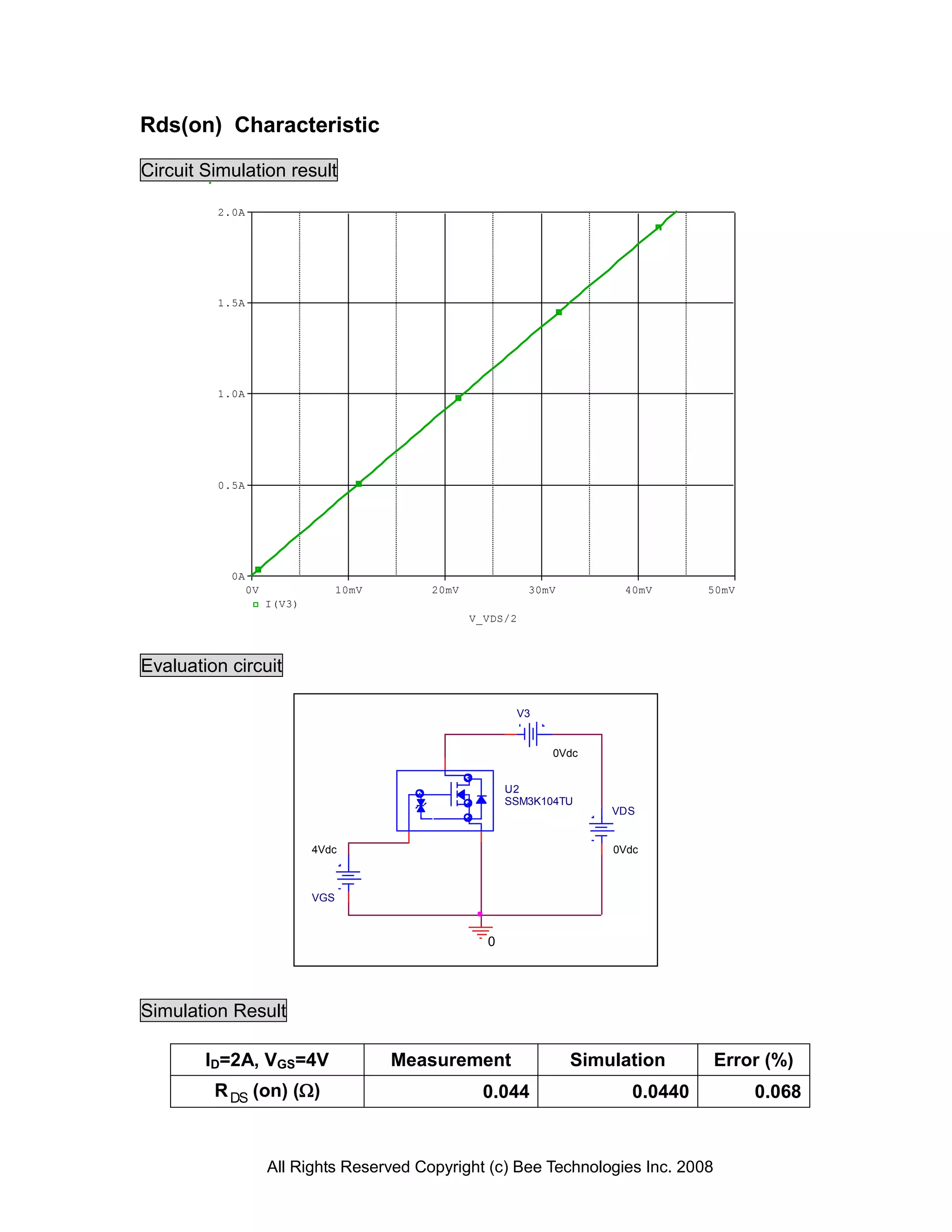
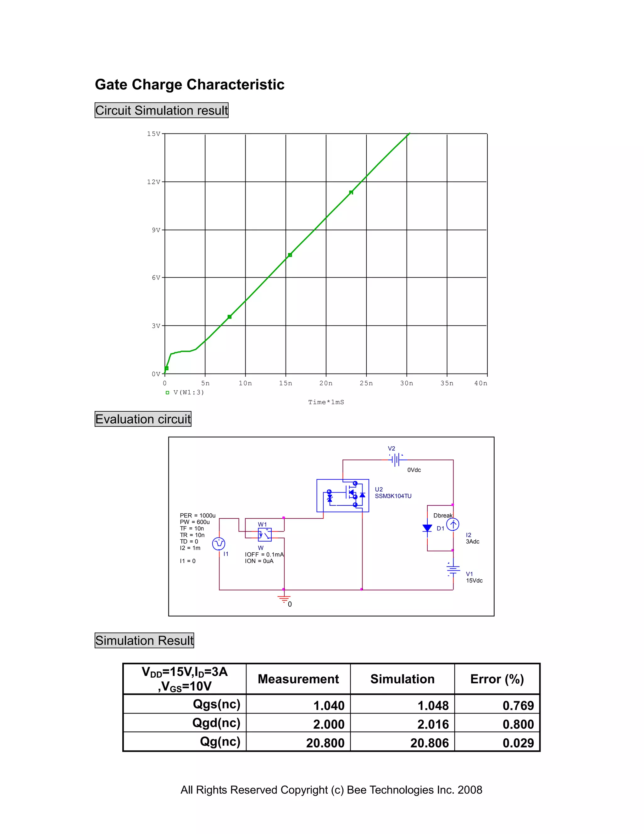
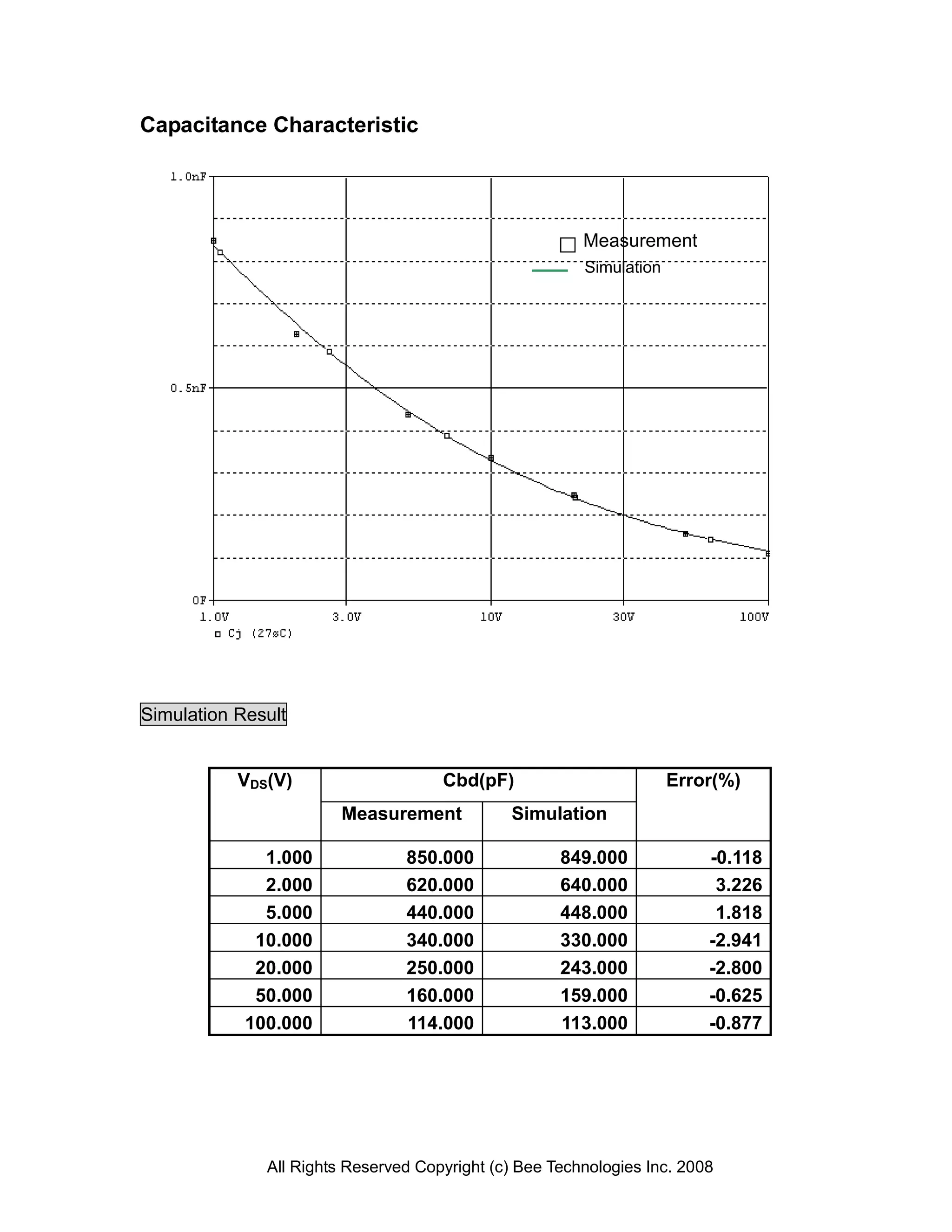
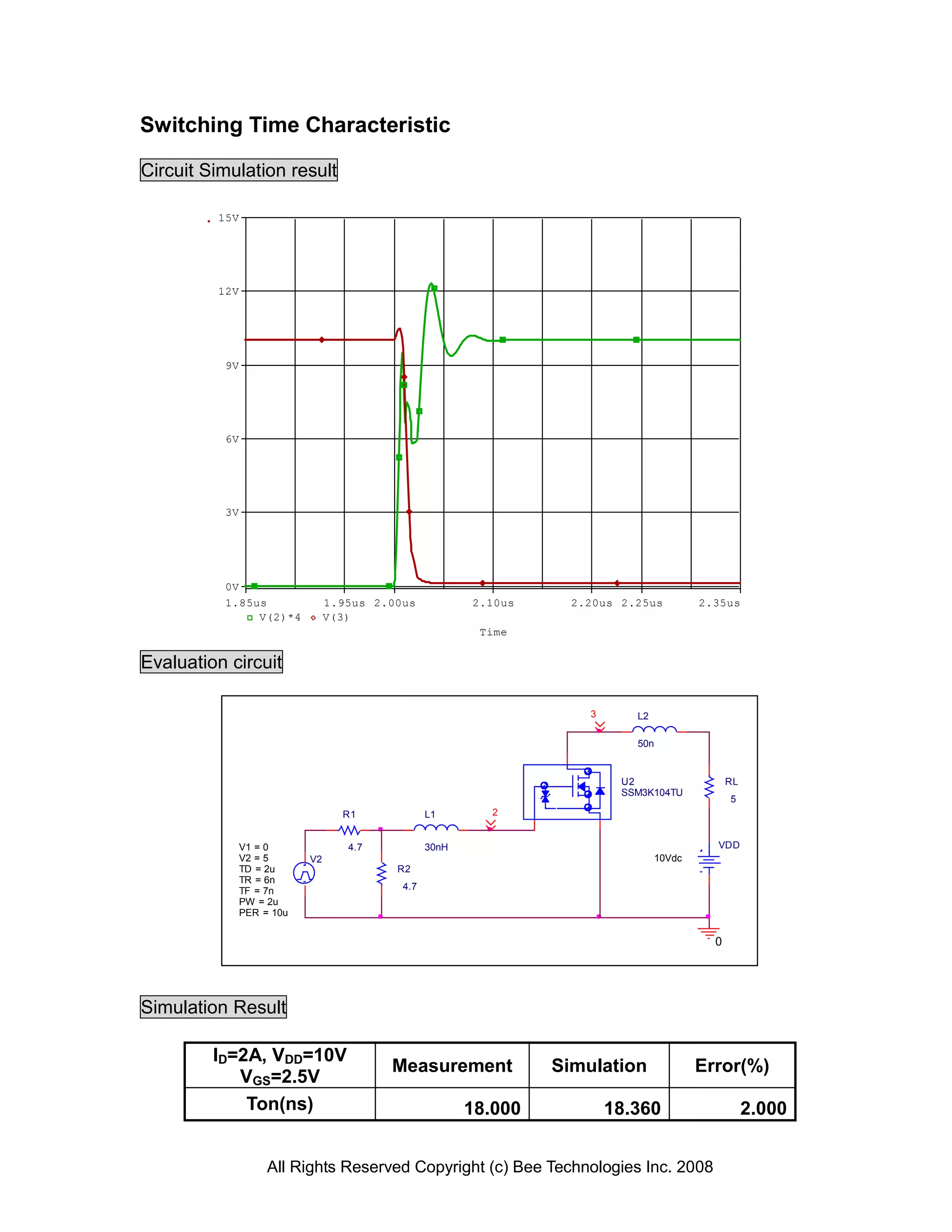
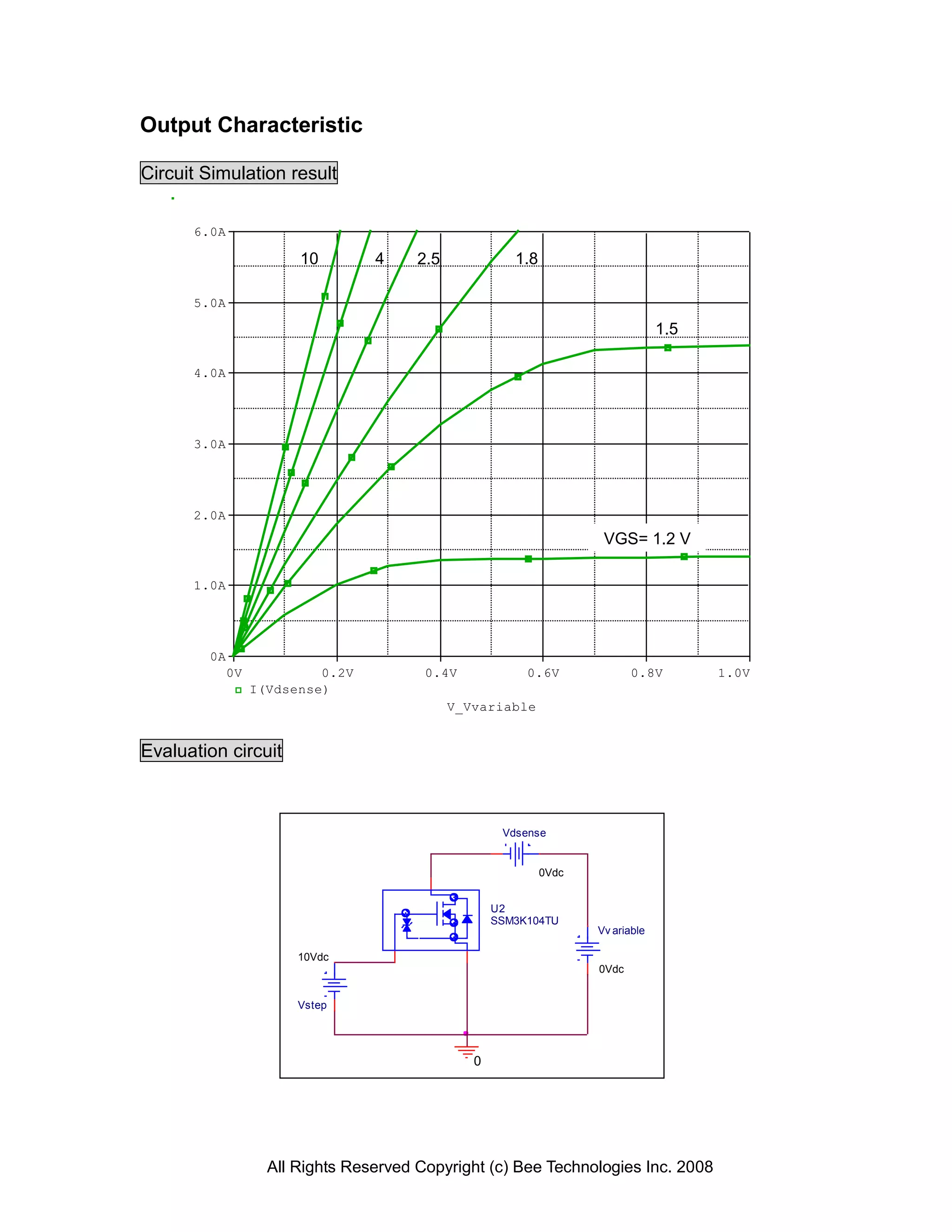
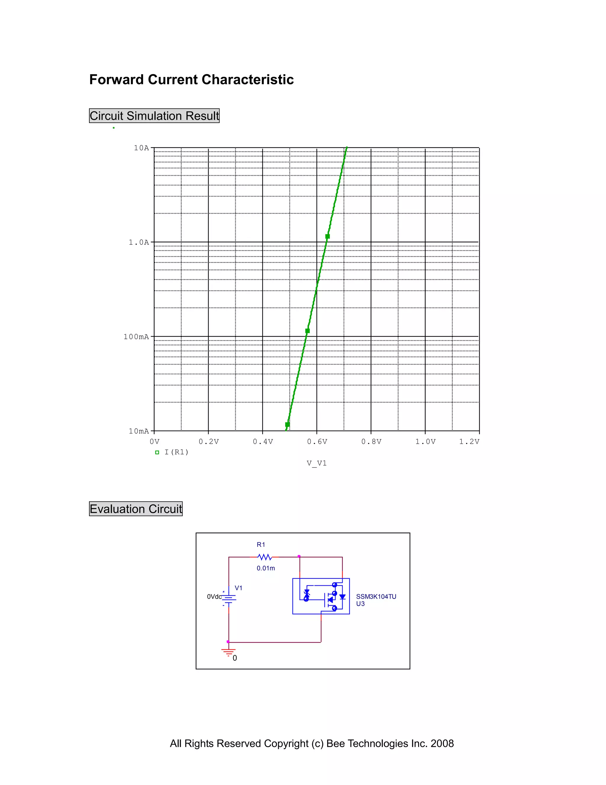
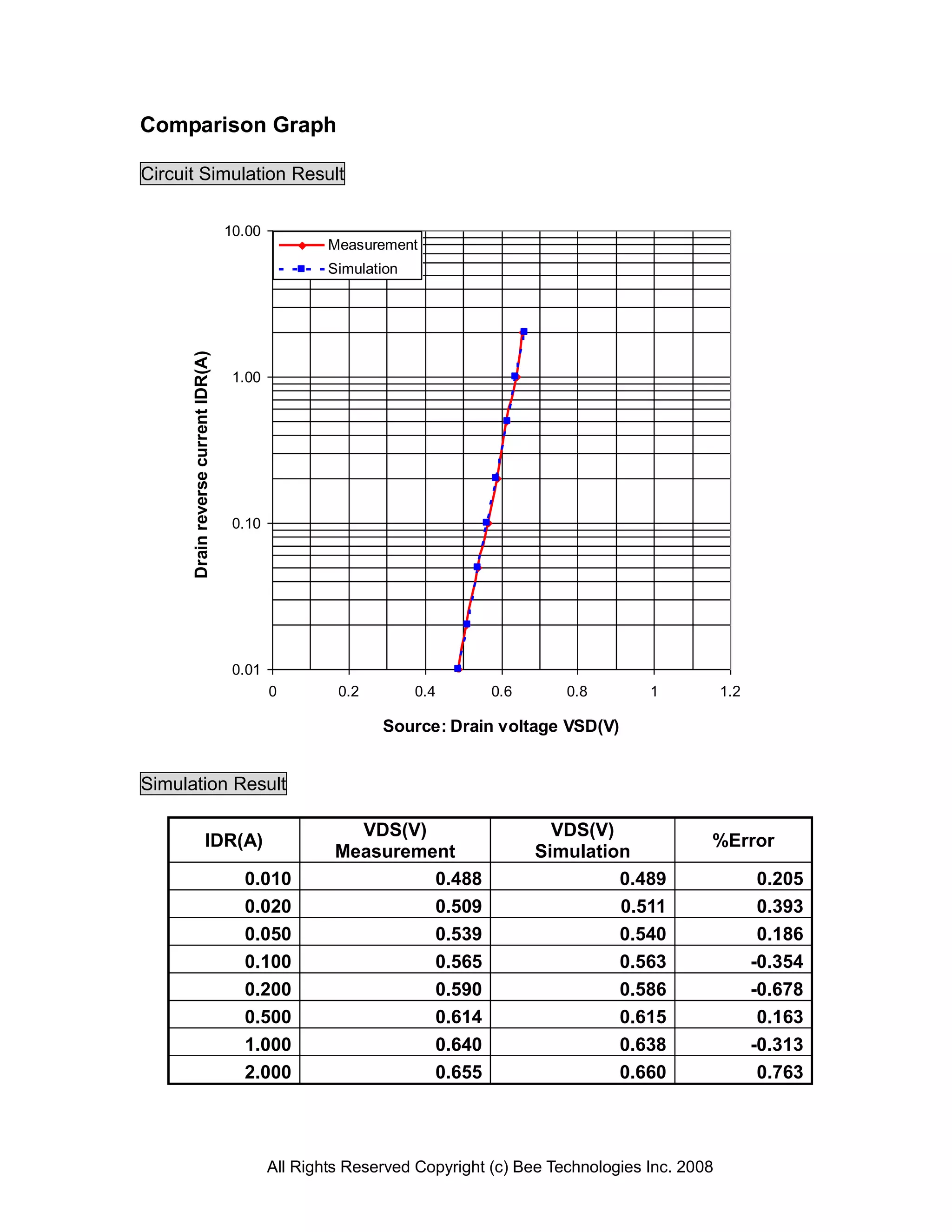
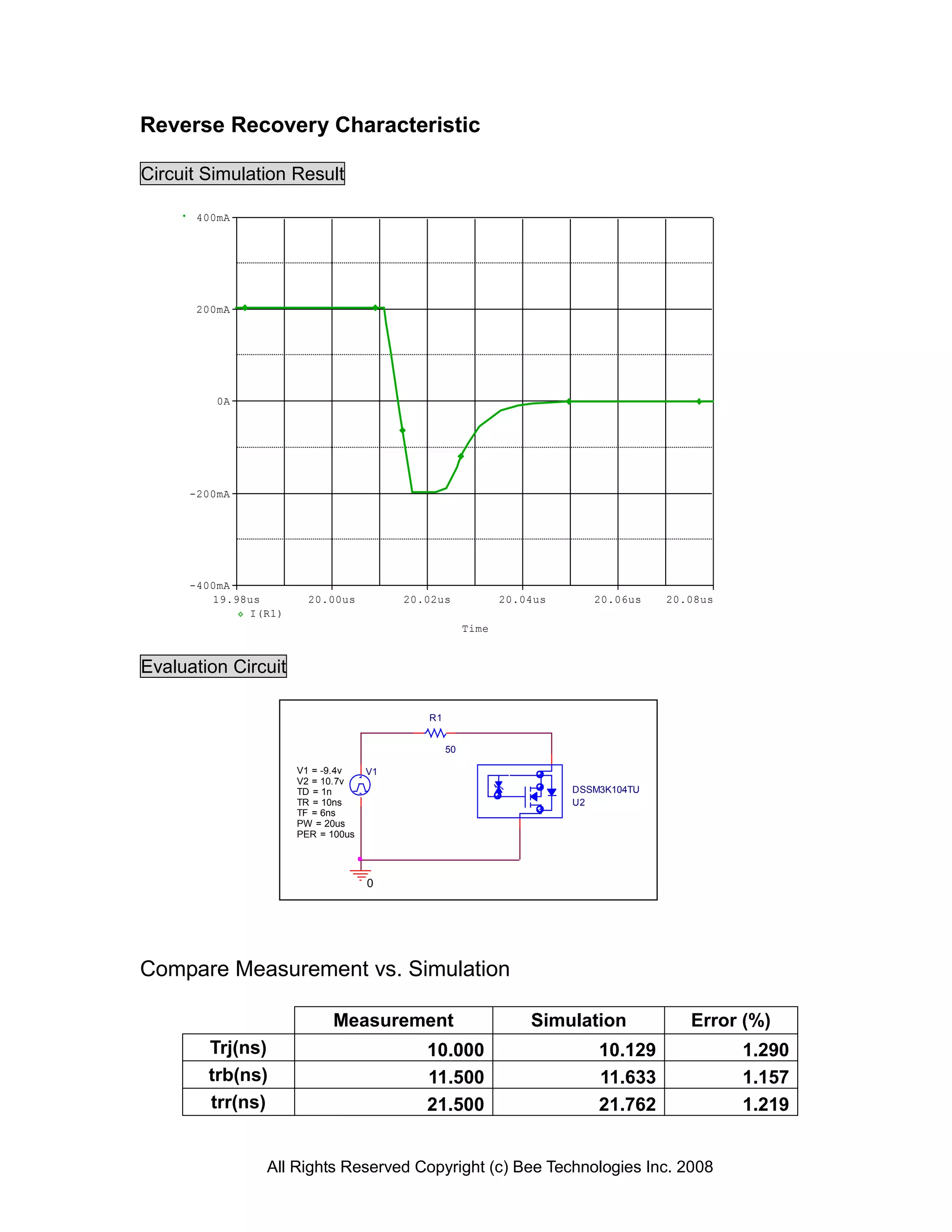
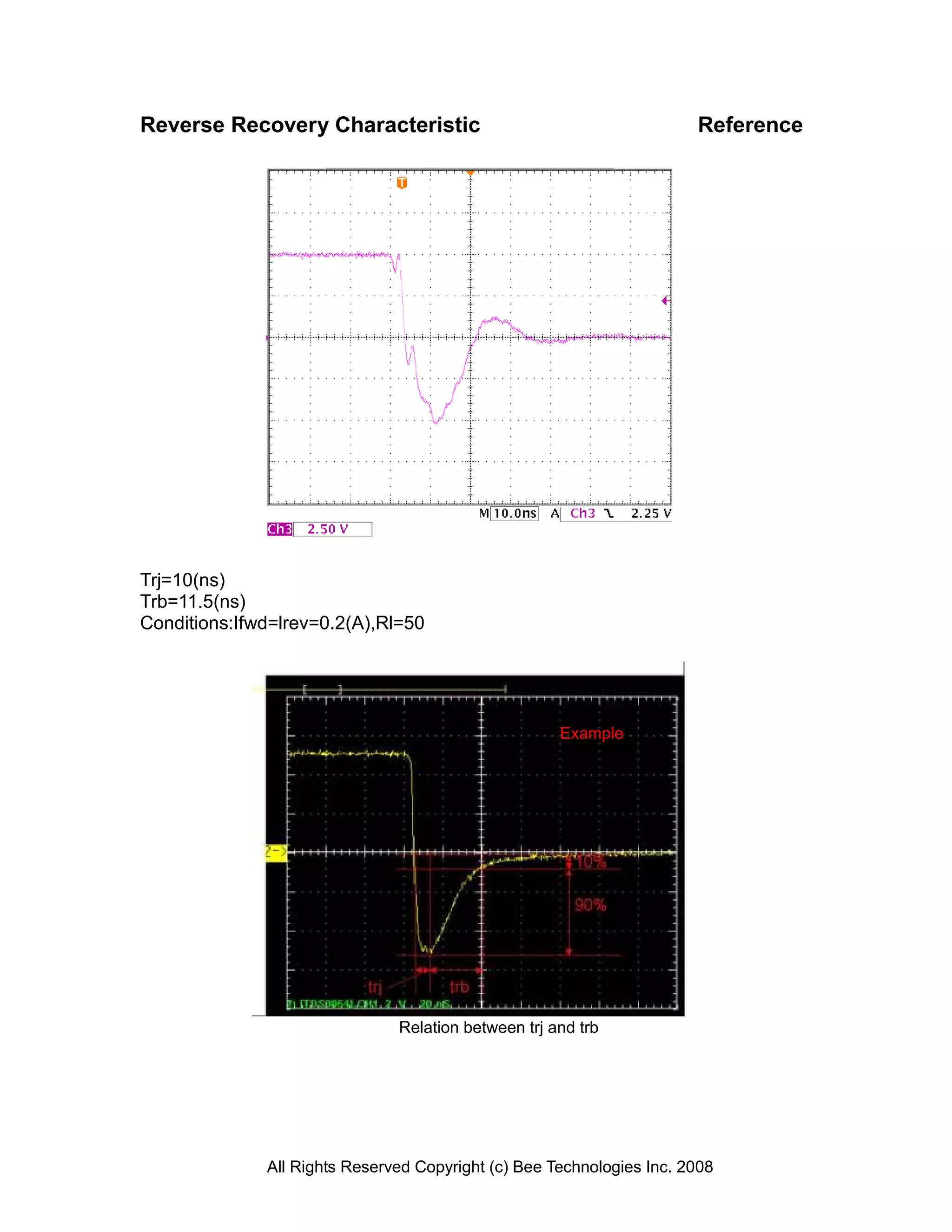
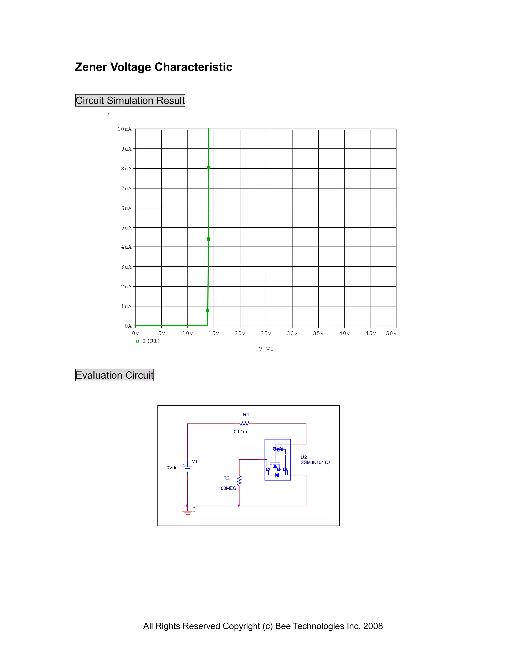
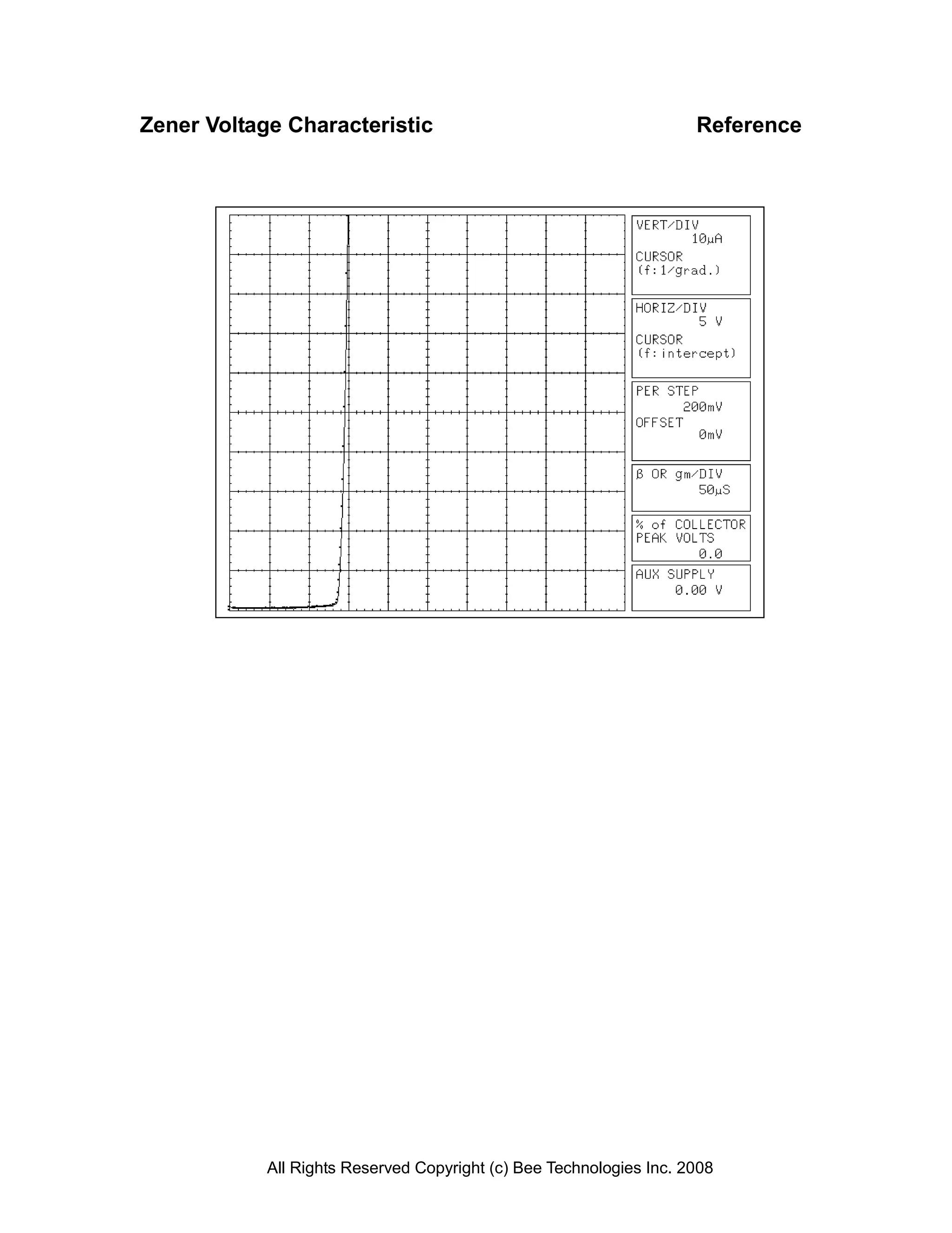

This document provides a device modeling report for a TOSHIBA SSM3K104TU power MOSFET. It includes: 1) Details of the MOSFET components and manufacturer. 2) A PSpice model listing parameters for the MOSFET. 3) Results of circuit simulations characterizing the MOSFET's transconductance, Vgs-Id relationship, Rds(on), gate charge, capacitance, switching time, output characteristics, forward/reverse currents, and zener voltage. Comparisons to measurement data show good agreement between simulation and measurement.


![Coded Agents – with UiPath SDK + LangGraph [Virtual Hands-on Workshop]](https://cdn.slidesharecdn.com/ss_thumbnails/codedagentsdeck-251215155422-5497c599-thumbnail.jpg?width=640&height=640&fit=bounds)


