Download to read offline
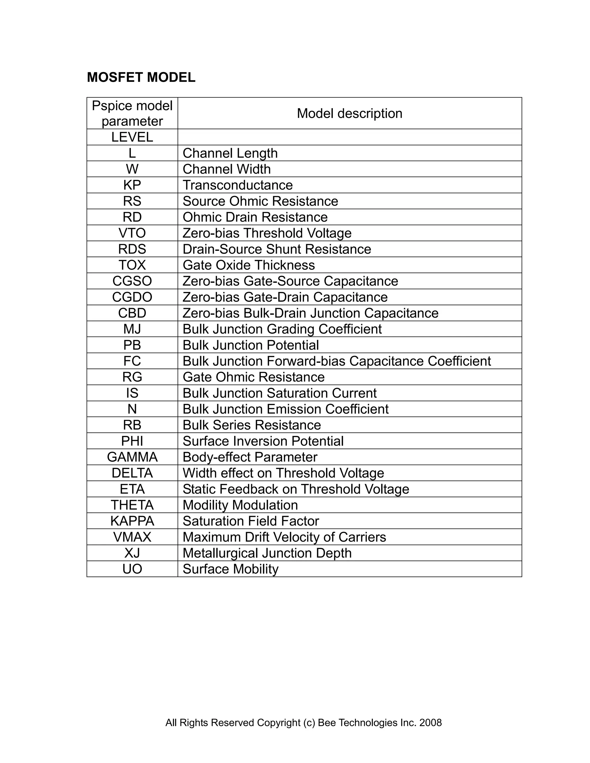
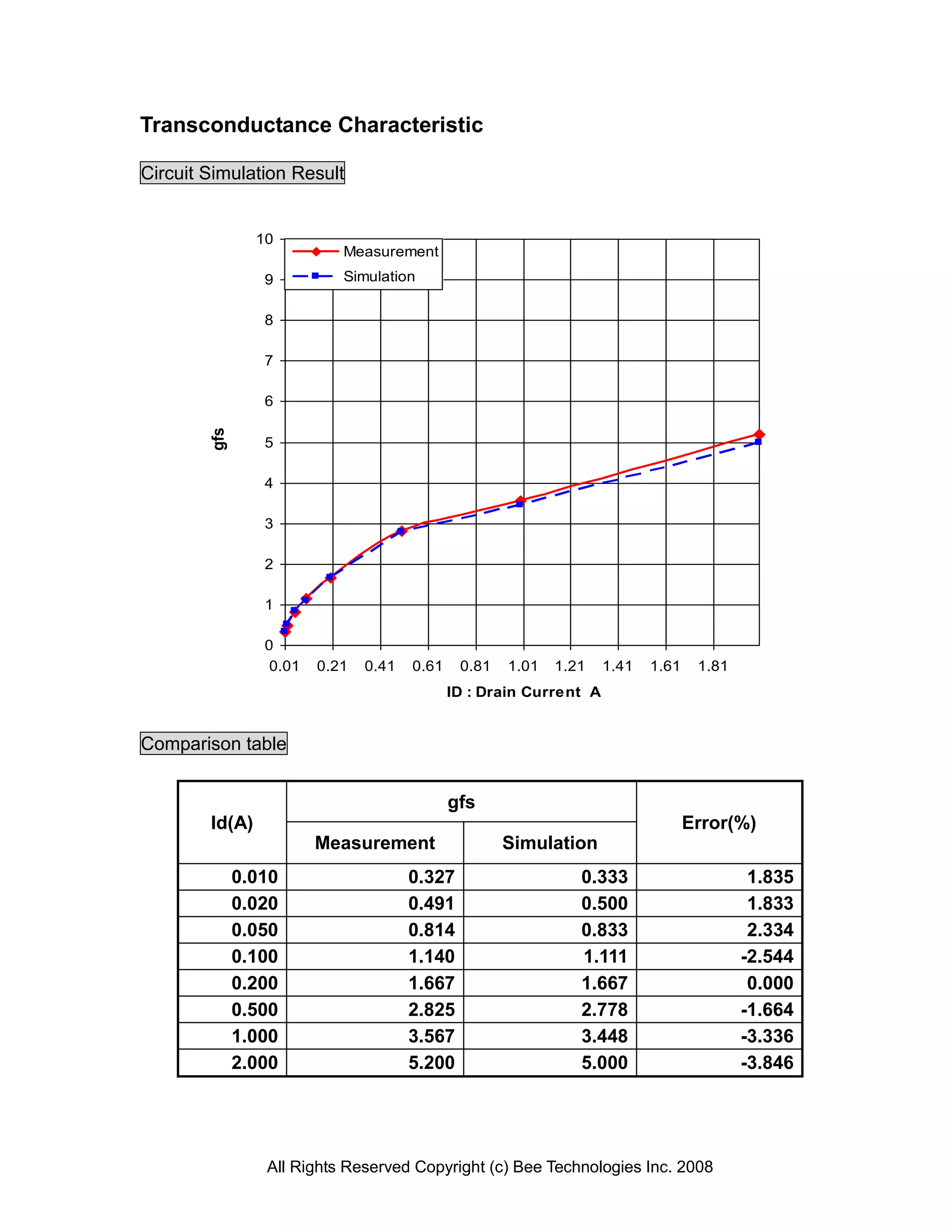
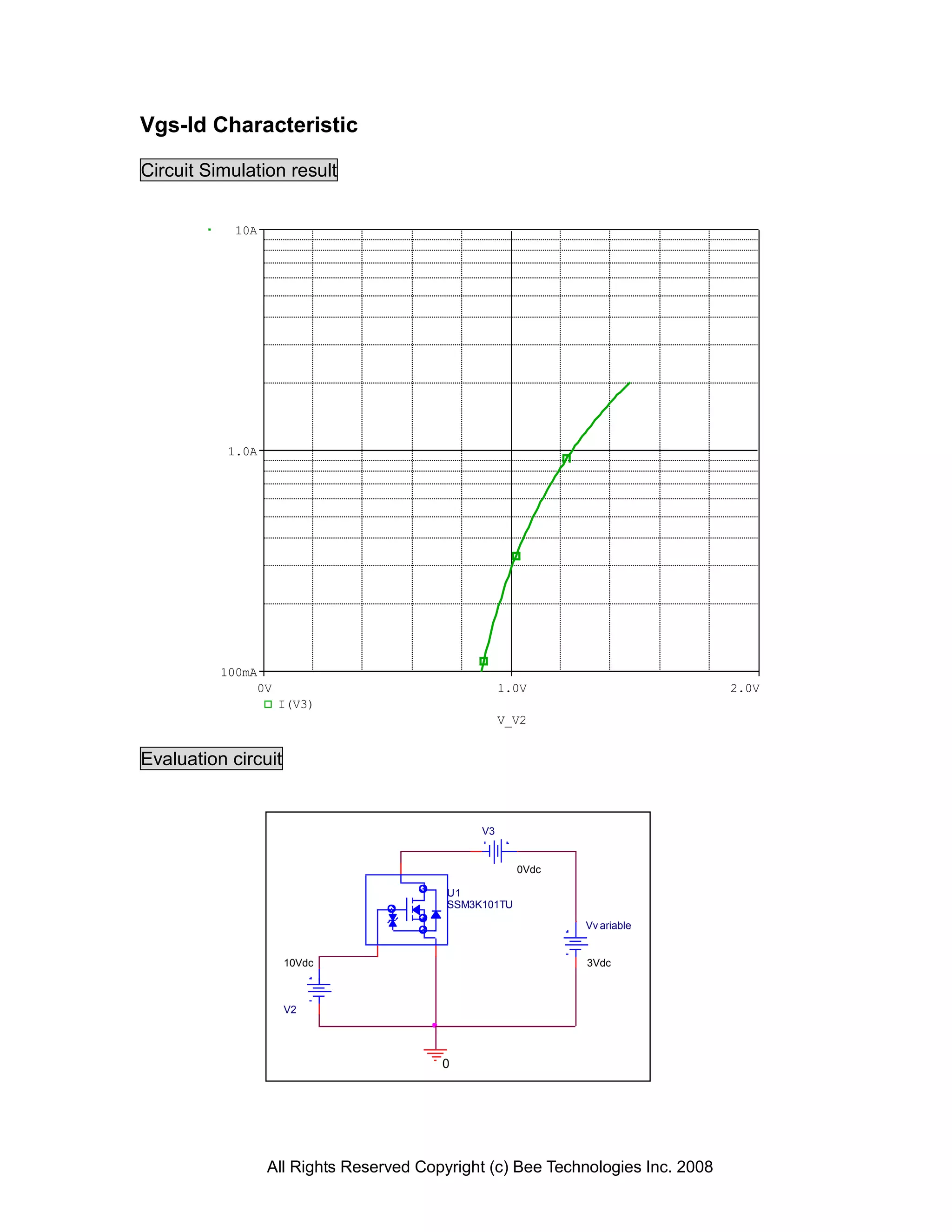
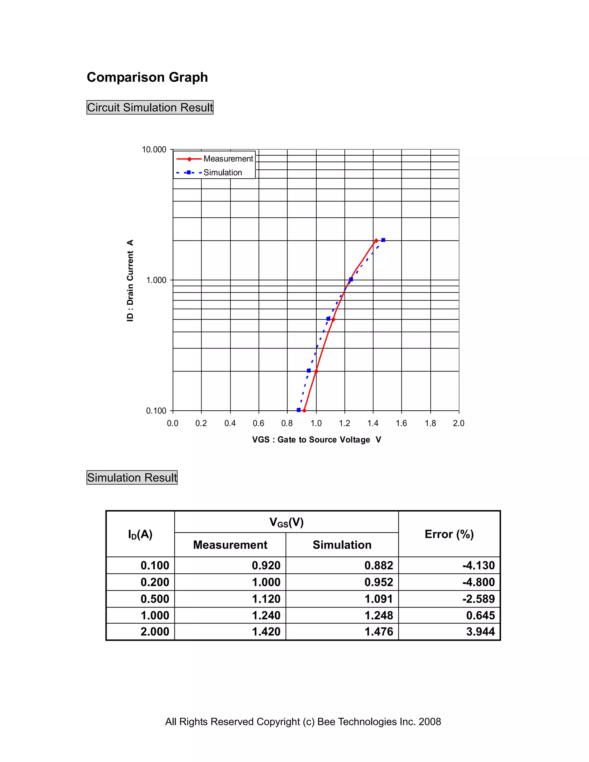
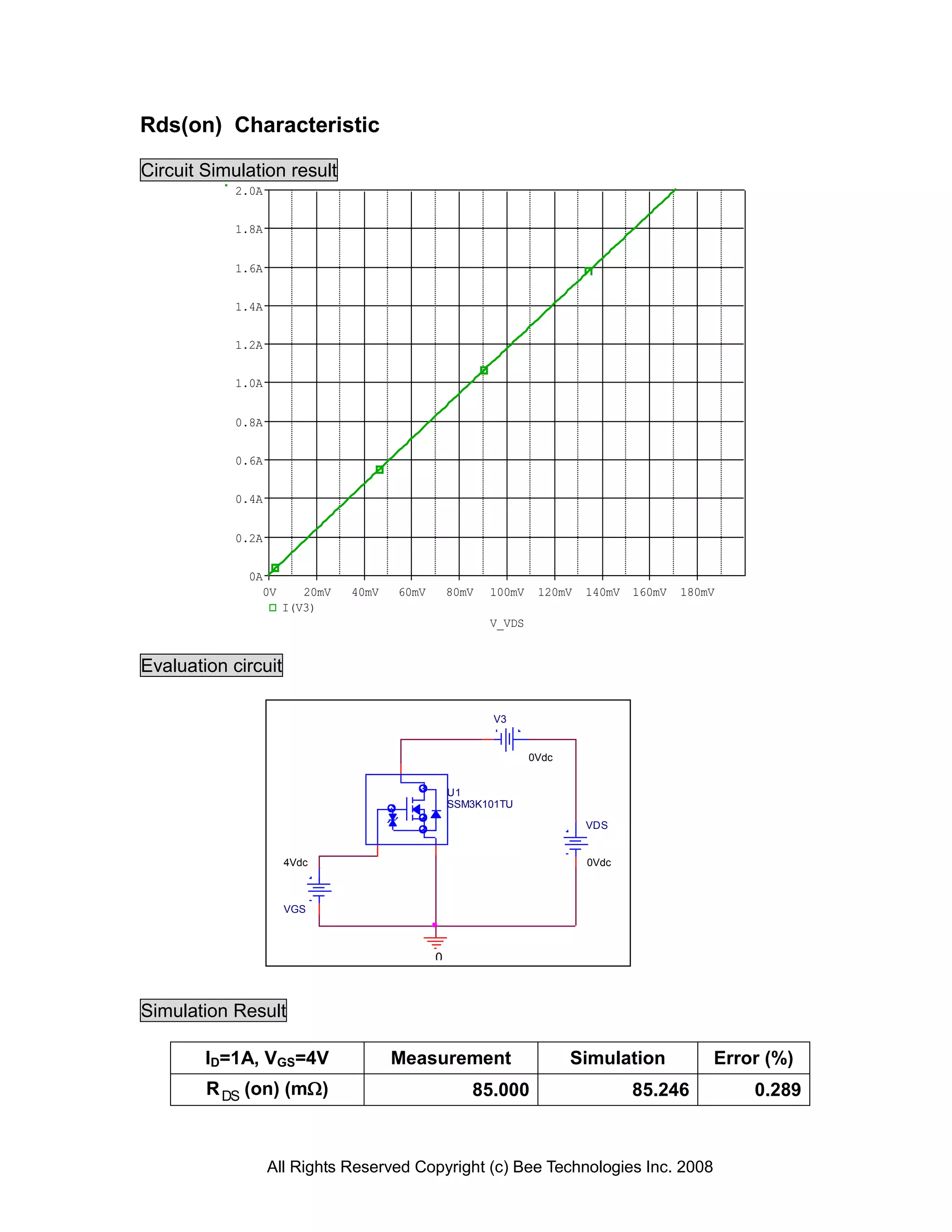
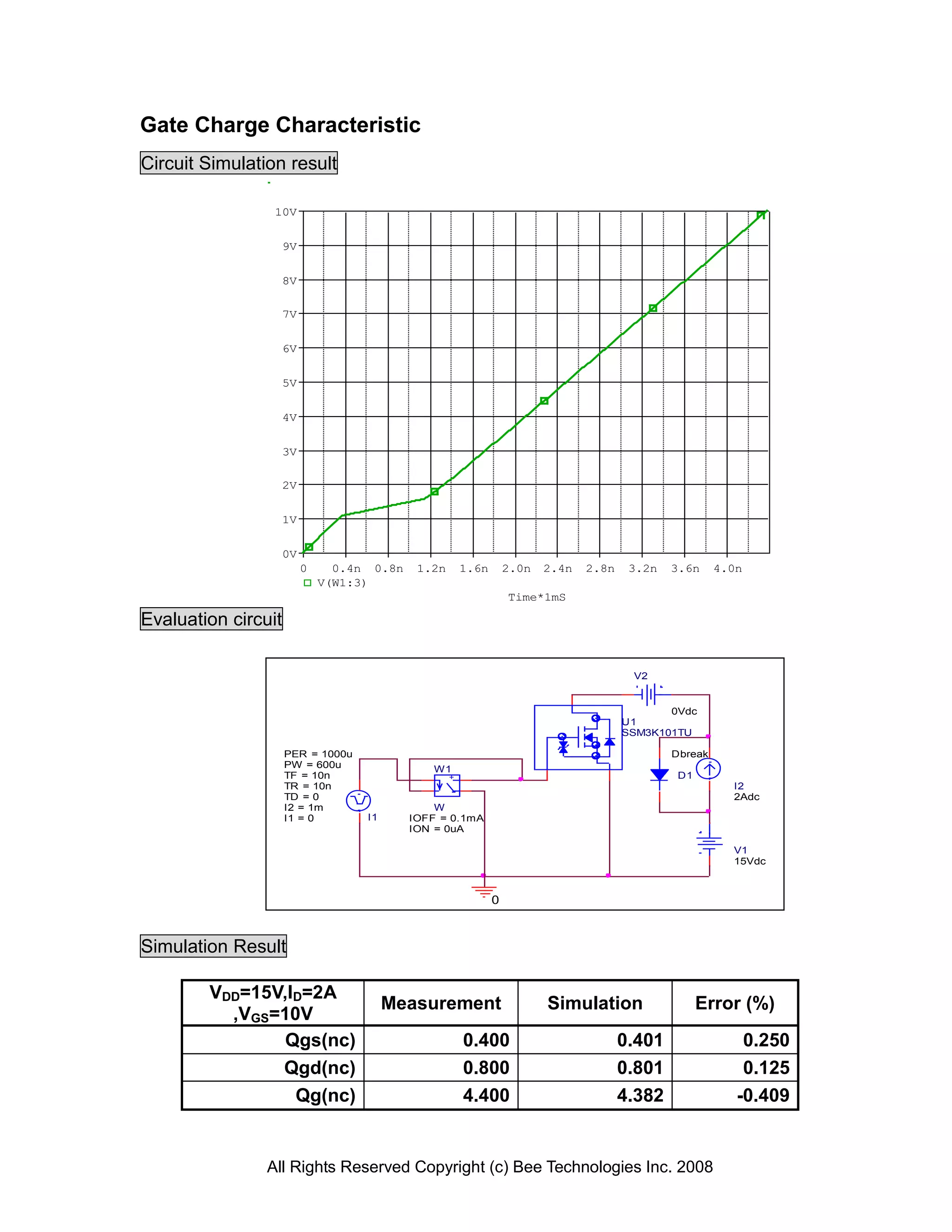
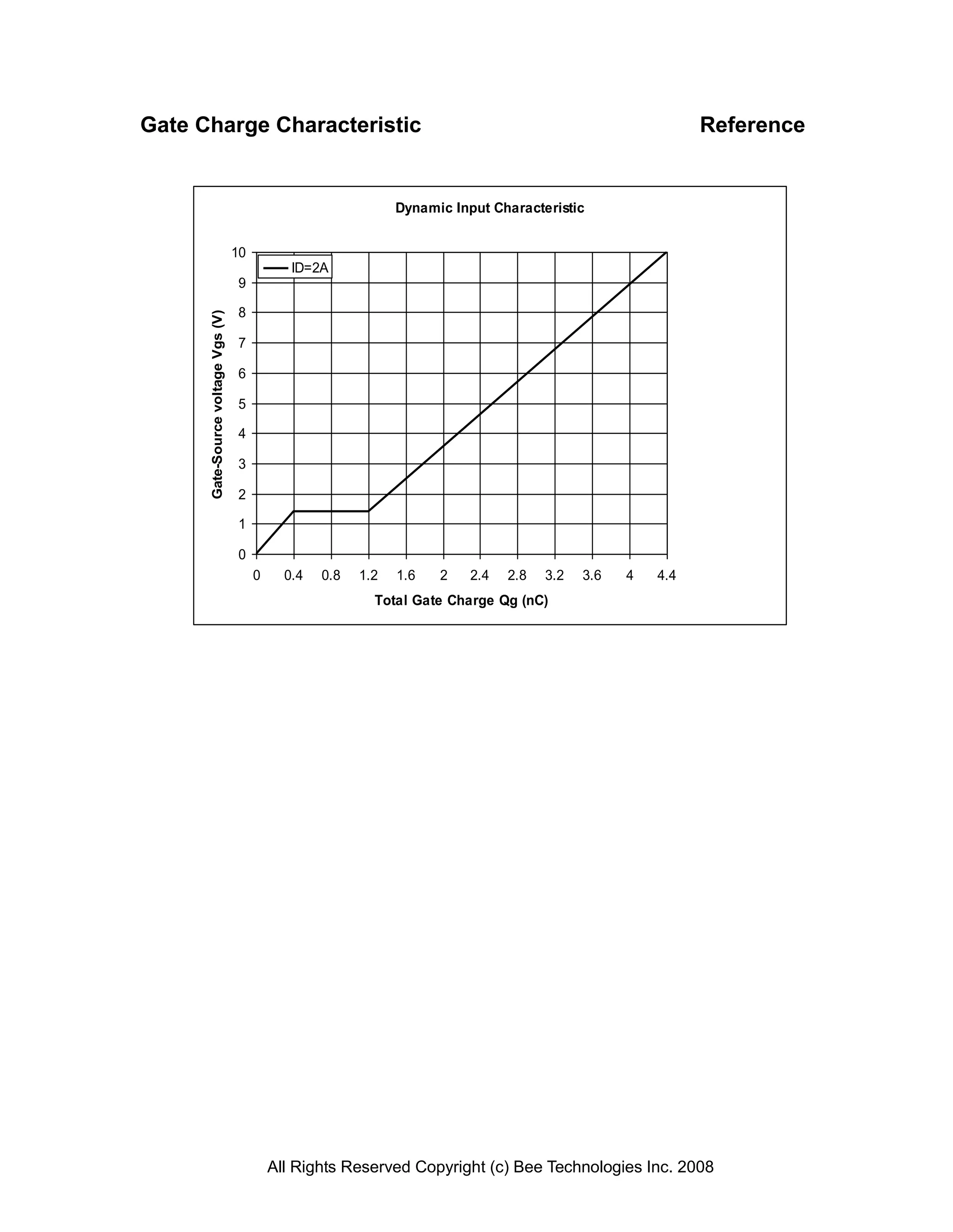
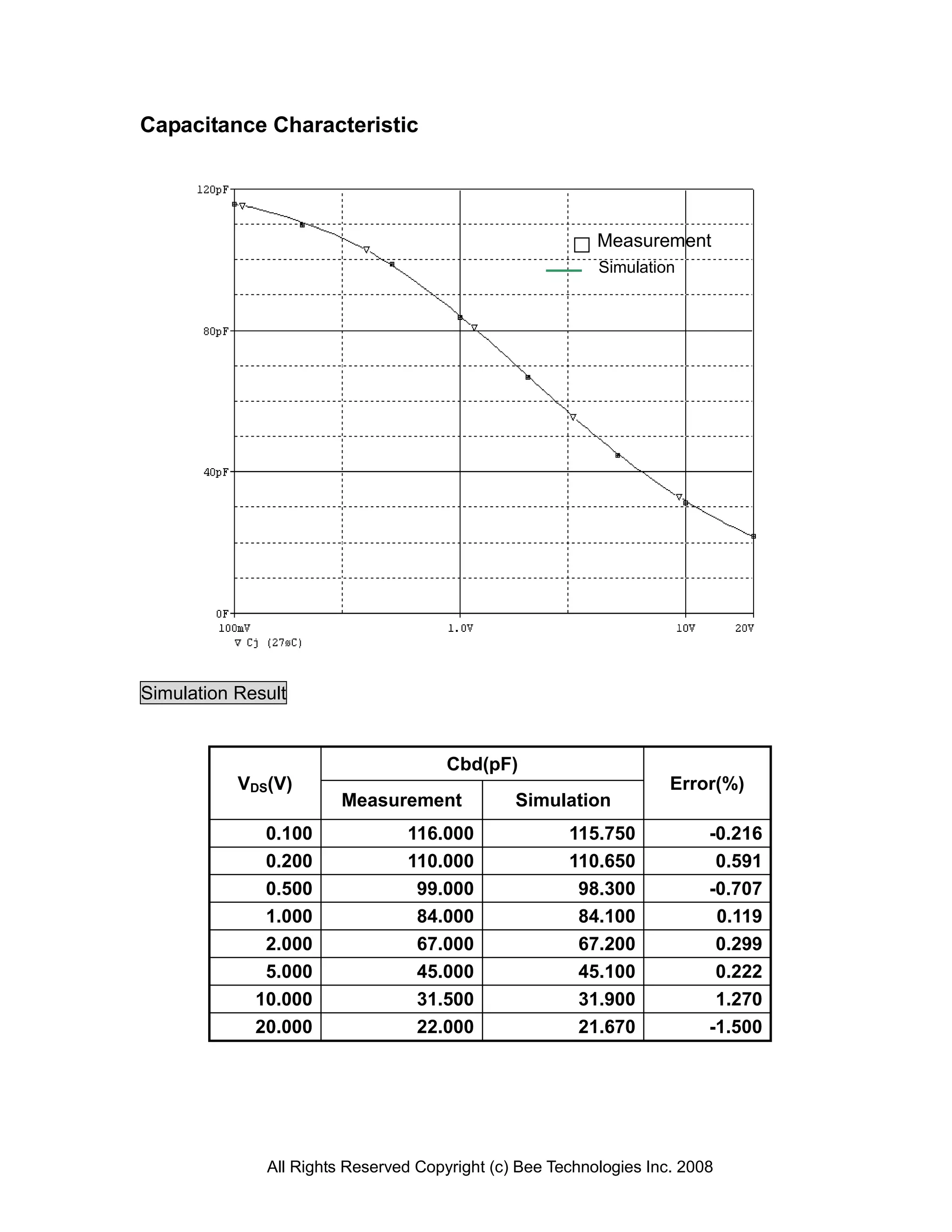
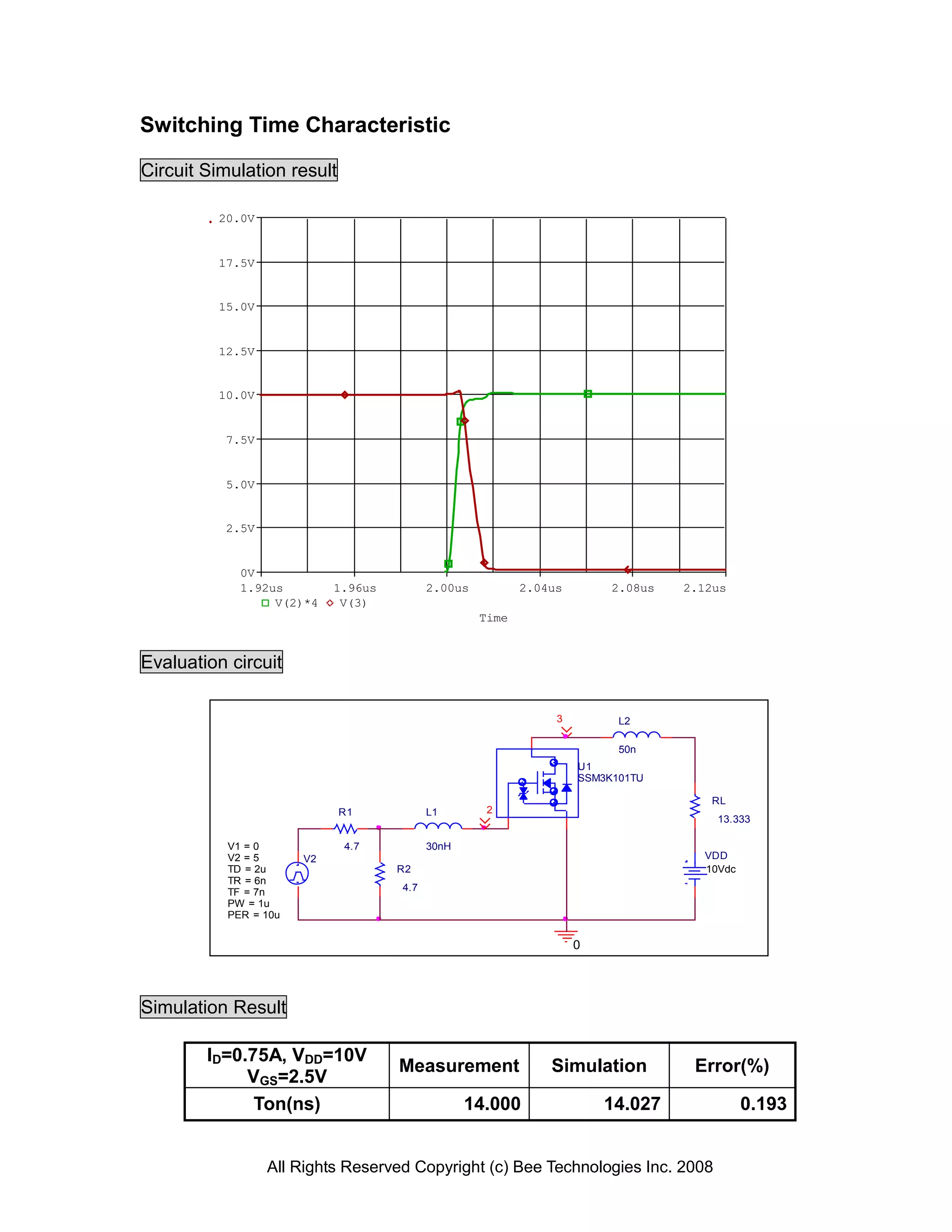
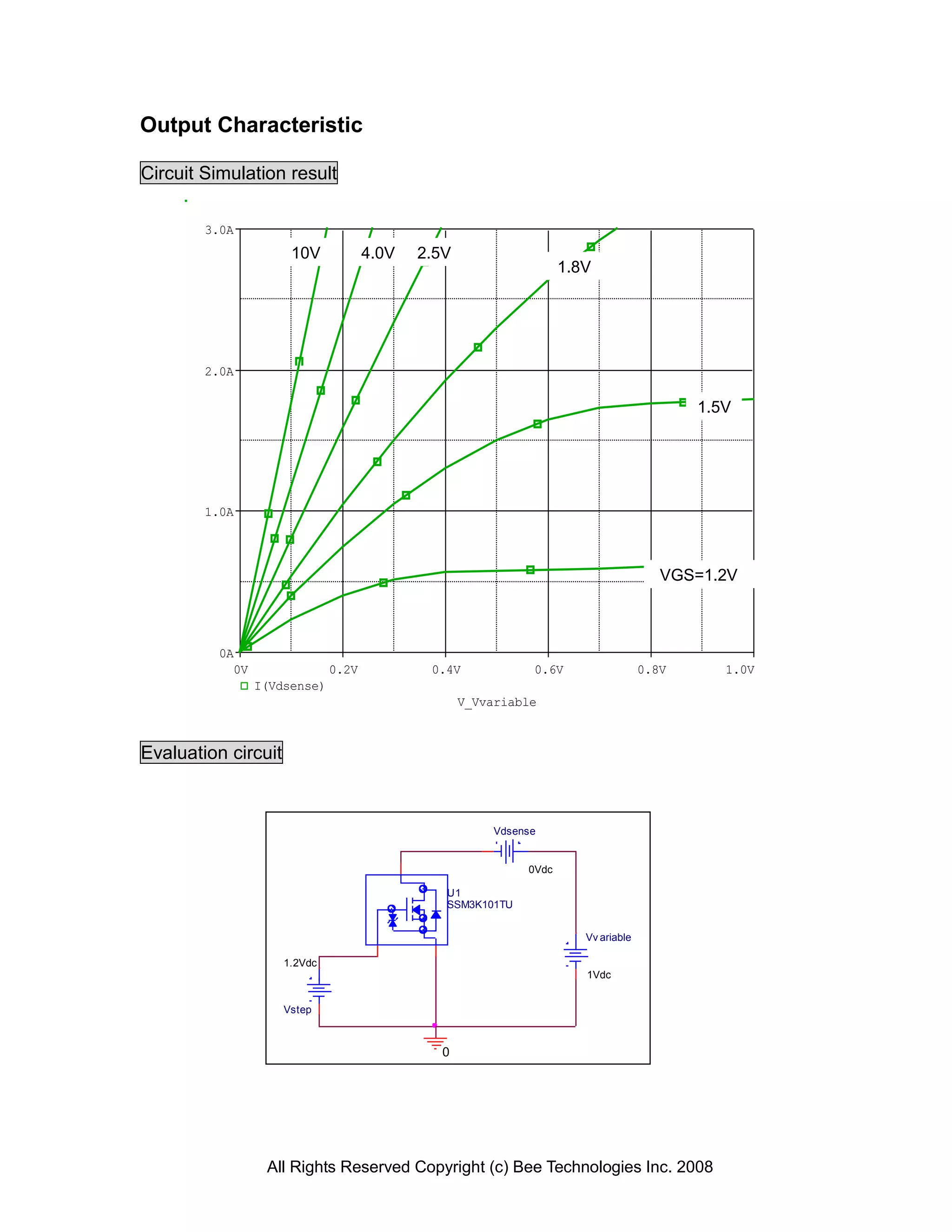
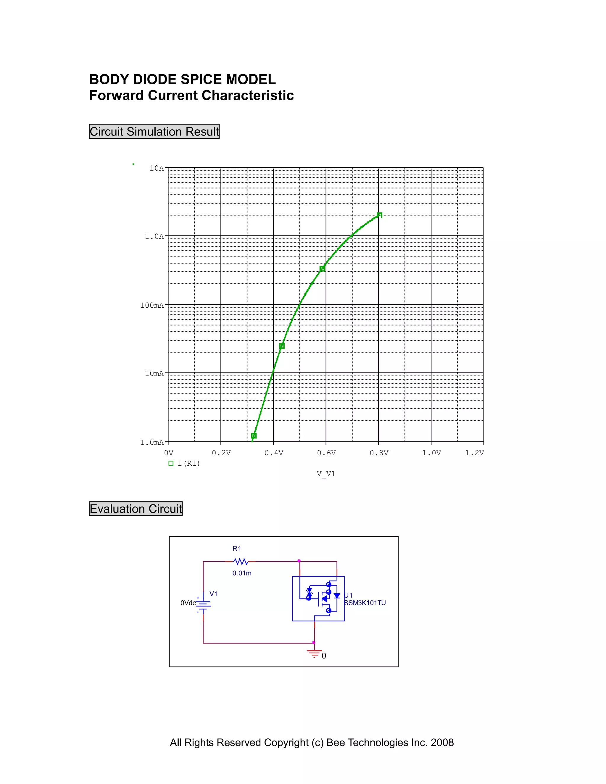
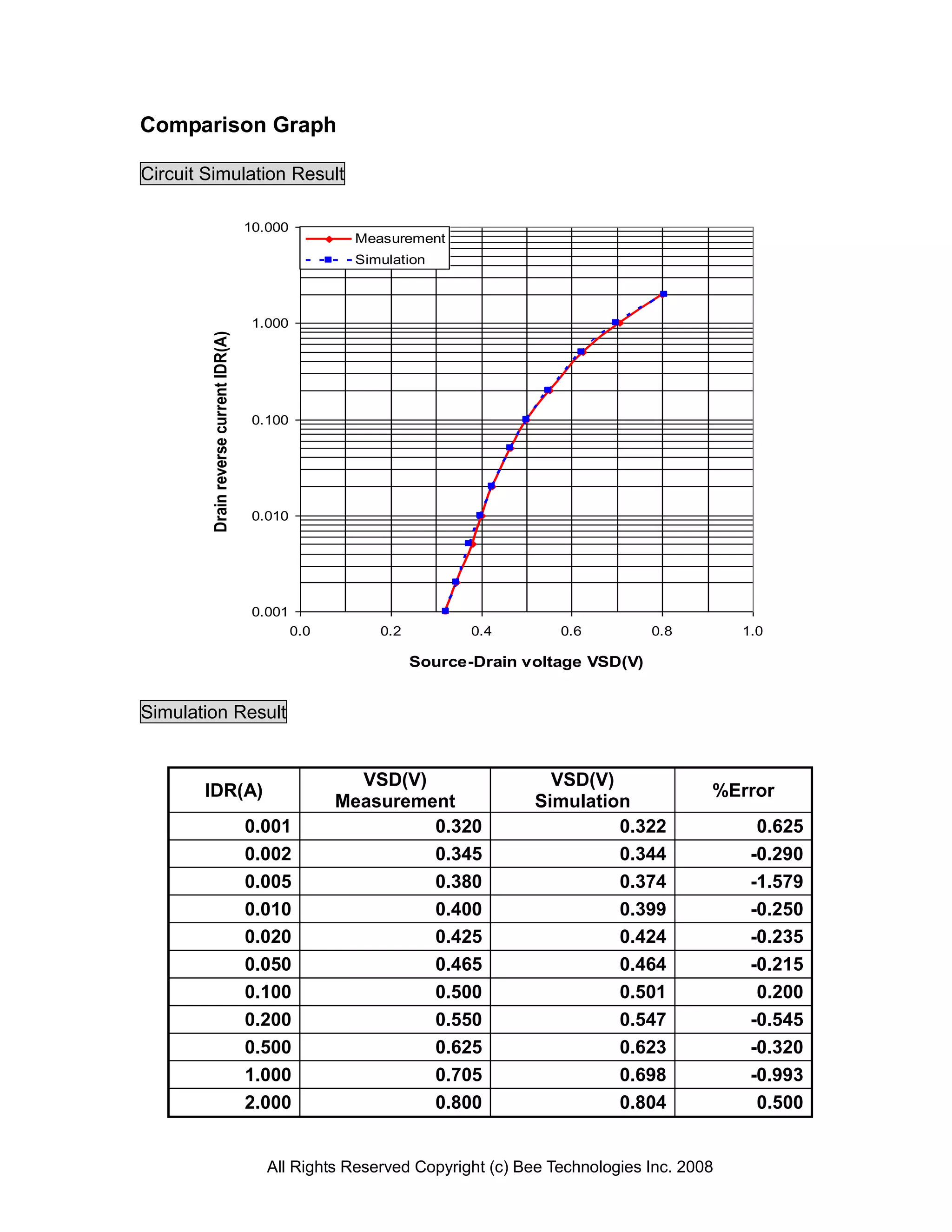
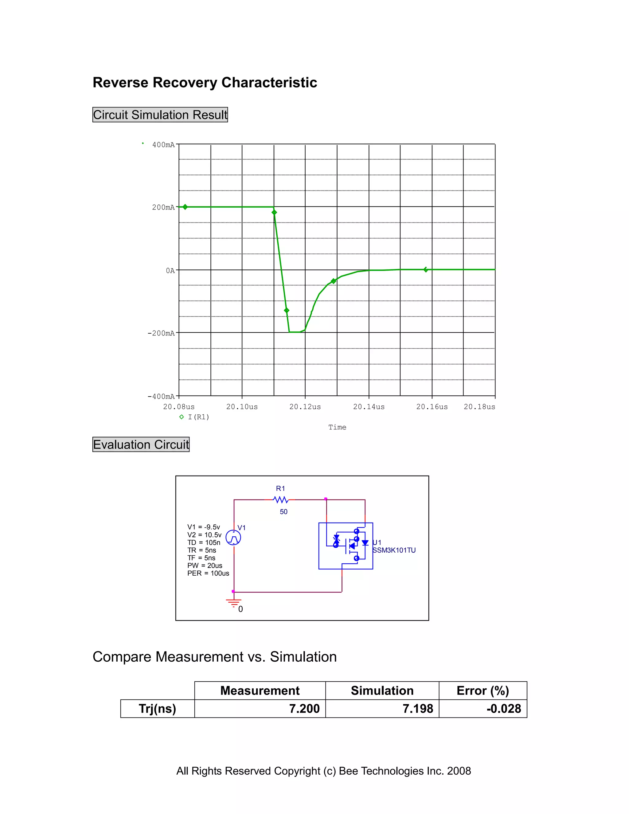
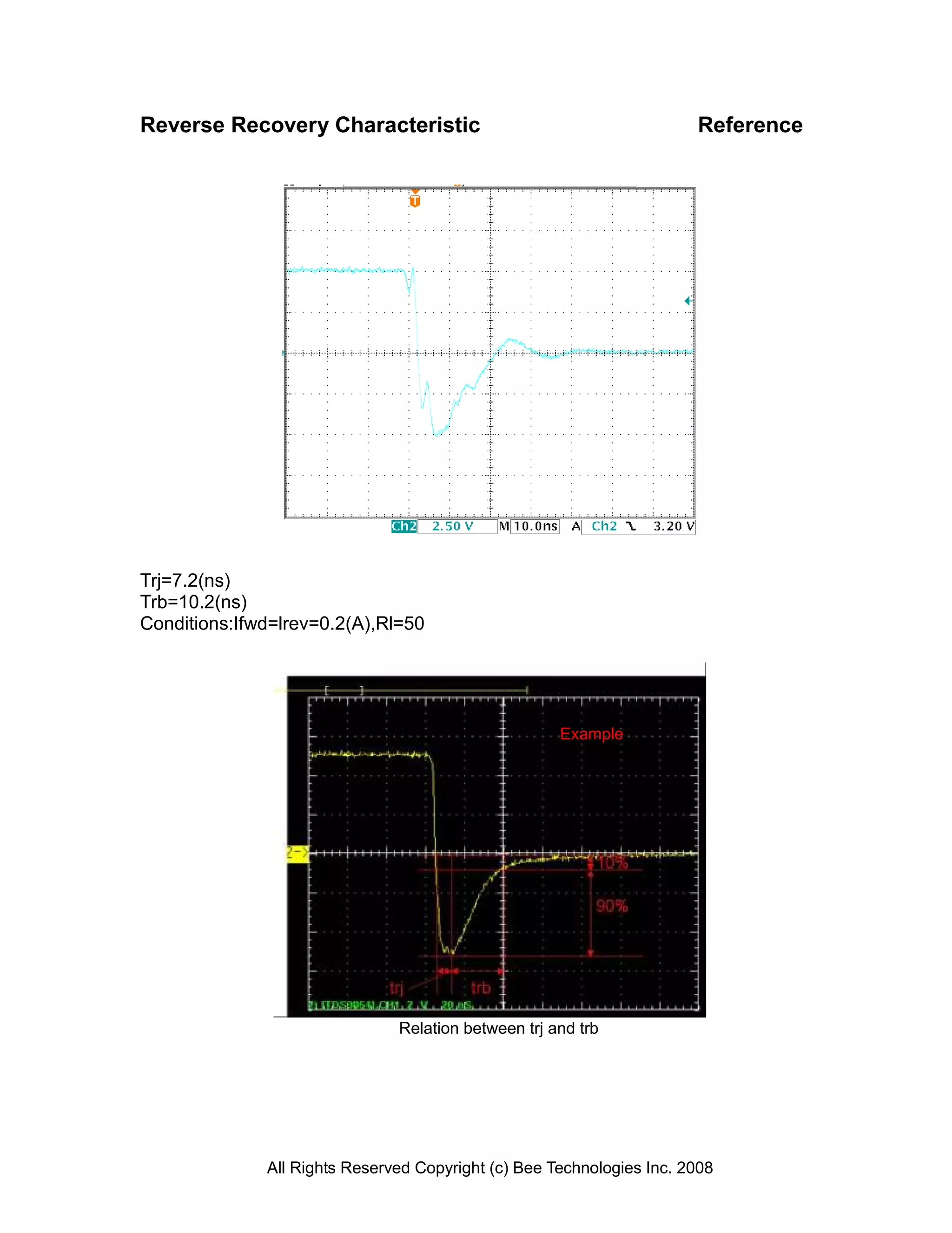
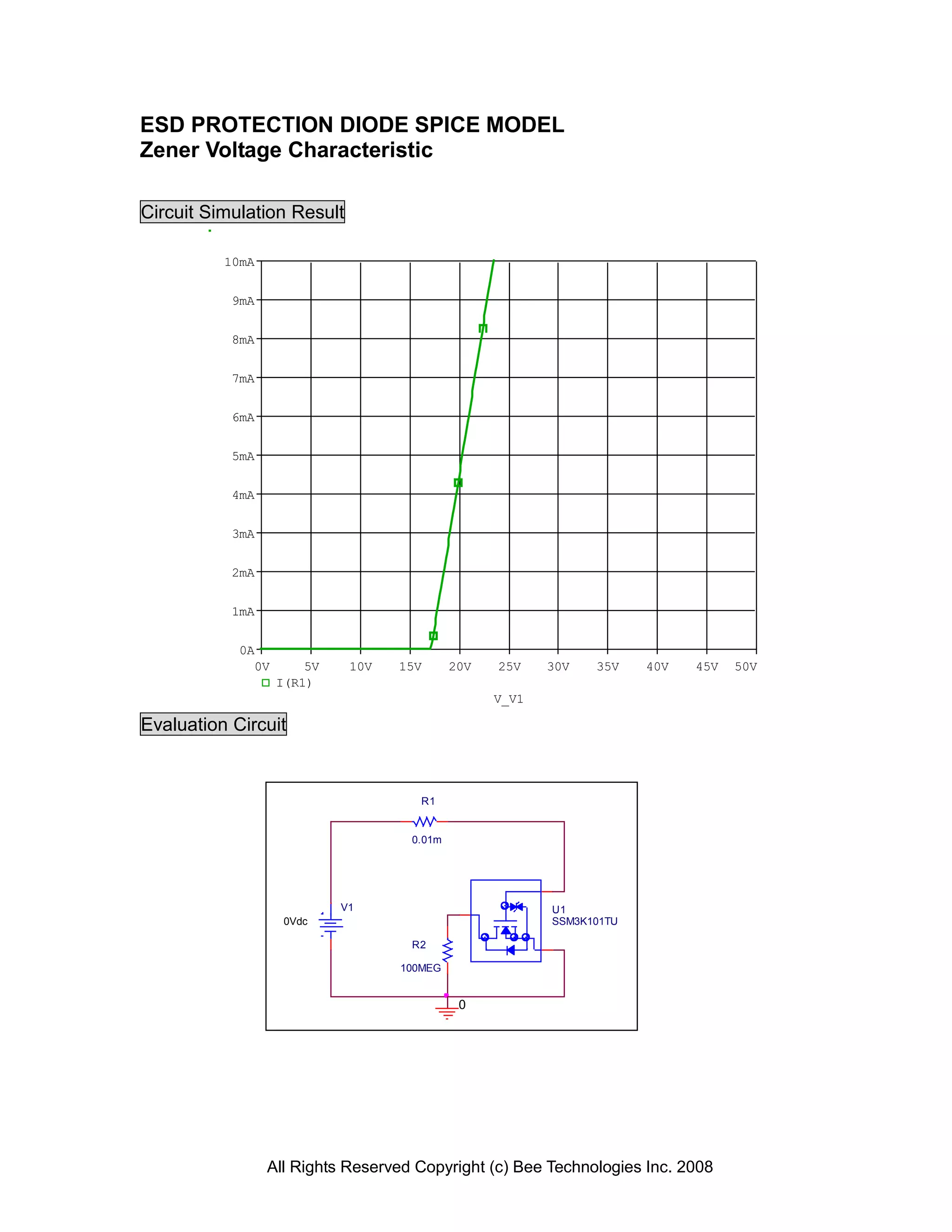
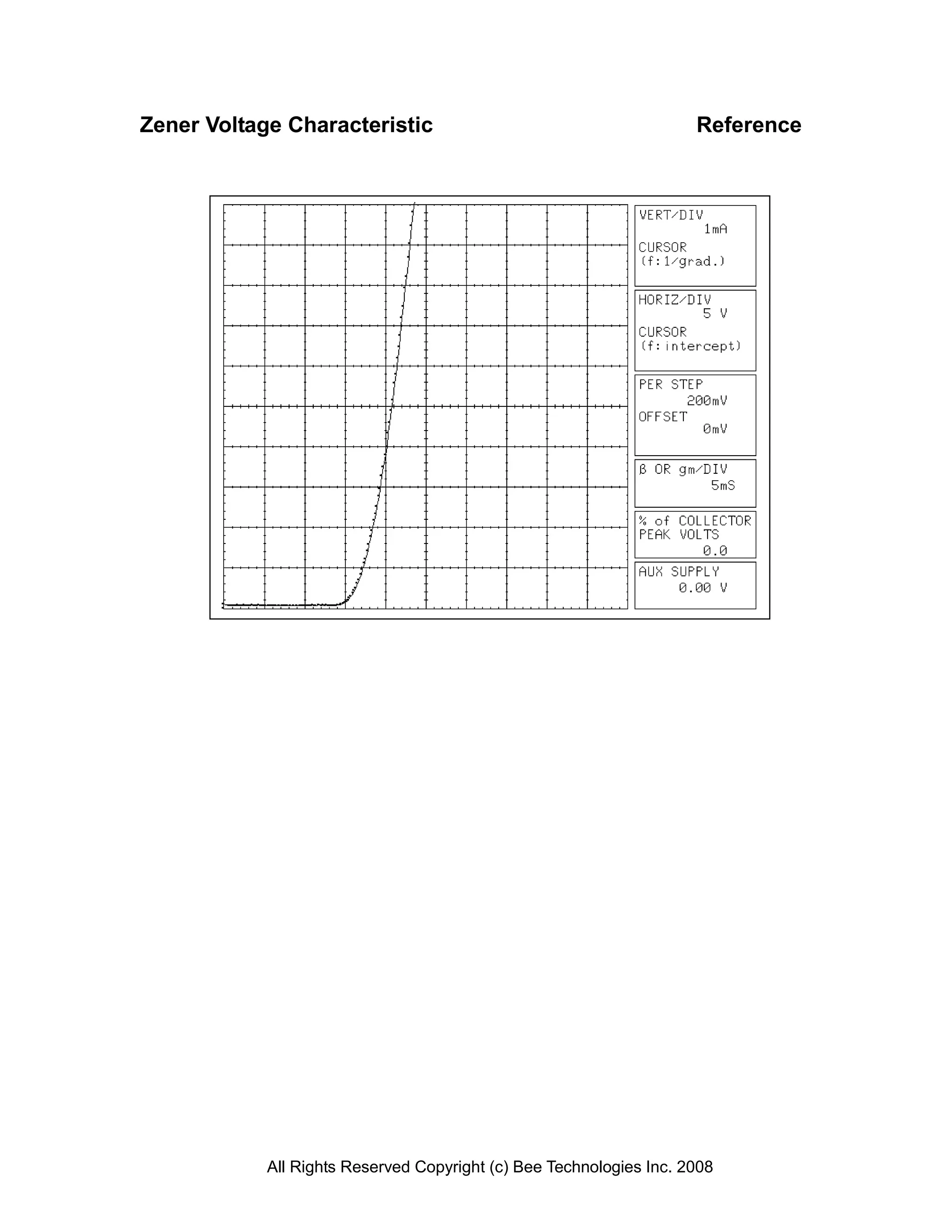

The document provides a device modeling report for a TOSHIBA SSM3K101TU power MOSFET and its internal body diode and ESD protection diode. It includes SPICE models and simulation results for the MOSFET characteristics like transconductance, gate charge, output, switching time and for the diode characteristics like forward current, reverse recovery and zener voltage. The simulations match well with measurements with less than 5% error for most characteristics.


![Coded Agents – with UiPath SDK + LangGraph [Virtual Hands-on Workshop]](https://cdn.slidesharecdn.com/ss_thumbnails/codedagentsdeck-251215155422-5497c599-thumbnail.jpg?width=640&height=640&fit=bounds)


