The document discusses field effect transistors (FETs), specifically junction FETs (JFETs). It contains the following key points:
1. JFET output characteristics show that drain current decreases with increasing reverse gate-source voltage, as the depletion region widens, reducing the channel width. At the gate-source cut-off voltage VGS(off), the channel is fully pinched off and drain current reaches zero.
2. Transfer characteristics relate drain current ID to gate-source voltage VGS. ID decreases quadratically with VGS and reaches zero at the pinch-off voltage VP, which is equal to VGS(off).
3. The document derives an expression for the depletion region width


![Integrating the above equation subject to boundary condition we get x to w
dv/dx = -[q ND/ ɛ ]*(x-w)
Integrating again
V = -(q ND/ɛ )* (x2/2 – w x)
V = -[q ND/2ɛ](x2- 2wx)
At x=w, V=VB which is the junction or barrier potential
VB = qNDW2/2ɛ
W2 = 2ɛ /qND *VB
W = {2ɛ/ qND *VB}1/2
As the barrier potential represents, a reverse voltage, it is lowered
by an applied forward voltage V(x) at x.
since; VB = VP-V(x)
Hence;
W(x) = a-h(x) = {2ɛ/ qNd*Vp-V(x)}1/2](https://image.slidesharecdn.com/session2-210603170749/75/Session-2-7-2048.jpg)
![Where ;
ɛ - dielectic constant of channel material
q - magnitude of electronic charge
V0 – junction contact potential at x
V(x) – is the applied potential across space charge region
a - metallurgical distance between the substrate and p+
a-h(x) – is the W(x) of depletion region into channel at point x
• If the drain current is zero h(x) and v(x) are independent to x and hence b(x) or h(x) = h. It we substitute
h(x)=h=0
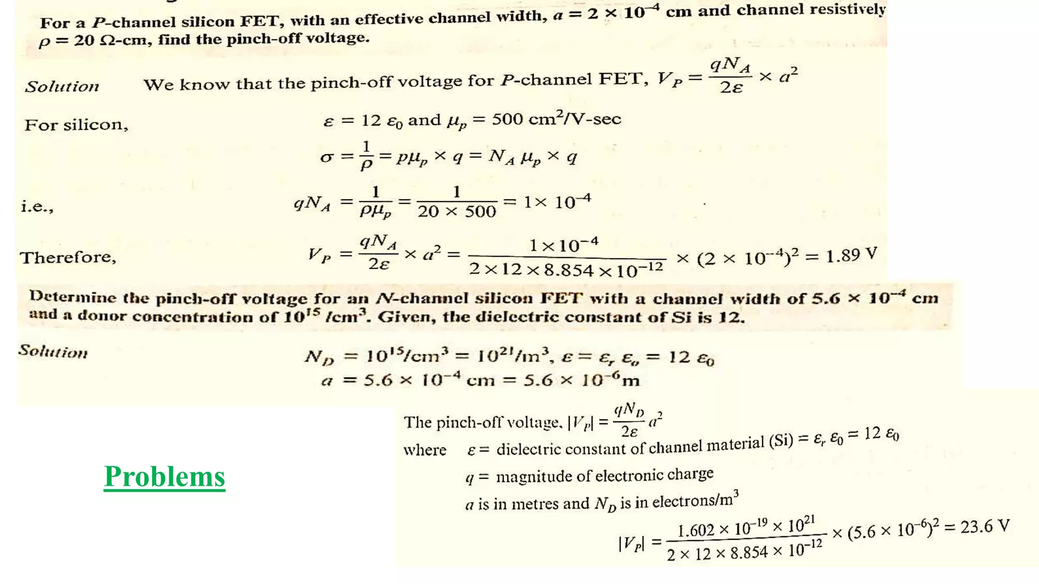
a = {(2ɛ/ qNd) * Vp}1/2
a2 = (2ɛ/ qNd)* Vp
|Vp| = (q N d/2ɛ) *a2
W(x) = a-h(x) = {2ɛ/ qNd*[Vp-V(x)]}1/2](https://image.slidesharecdn.com/session2-210603170749/75/Session-2-8-2048.jpg)
![Expression for Drain Current (ID)
The relation between IDSS and VP is shown in Fig. We note that gate-source cut off voltage [i.e. VGS (off)] on
the transfer characteristic is equal to pinch off voltage VP on the drain characteristic i.e.
The transfer characteristic of JFET shown in Fig. a is part of a parabola. A rather complex mathematical
analysis yields the following expression for drain current
Where
ID= drain current at given VGS
IDSS= shorted – gate drain current
VGS= gate–source voltage
VGS (off)= gate–source cut off voltage](https://image.slidesharecdn.com/session2-210603170749/75/Session-2-10-2048.jpg)