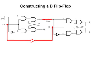
The document covers the topic of digital logic related to counters and flip-flops, detailing various circuit diagrams and their functions. It includes constructs for D flip-flops, shift registers, synchronous and asynchronous counters, and examples of modulo counters. Also mentioned are practical aspects such as enable and clear capabilities for digital systems.


![[ Figure 5.7a from the textbook ]
Circuit Diagram for the Gated D Latch](https://image.slidesharecdn.com/32counters-250207202655-c08c259e/85/Lecture-digital-logic-design-32_Counters-ppt-5-320.jpg)


![(a) Circuit
D Q
Q
Master Slave
D
Clock
Q
Q
D Q
Q
Qm Qs
Clk
Clk
[ Figure 5.9a from the textbook ]
Master-Slave D Flip-Flop](https://image.slidesharecdn.com/32counters-250207202655-c08c259e/85/Lecture-digital-logic-design-32_Counters-ppt-11-320.jpg)


![A simple shift register
[ Figure 5.17 from the textbook ]
D Q
Q
Clock
D Q
Q
D Q
Q
D Q
Q
In Out
t0
t1
t2
t3
t4
t5
t6
t7
1
0
1
1
1
0
0
0
0
1
0
1
1
1
0
0
0
0
1
0
1
1
1
0
0
0
0
1
0
1
1
1
0
0
0
0
1
0
1
1
Q1 Q2 Q3 Q4 Out
=
In
(b) A sample sequence
(a) Circuit
Q1 Q2 Q3 Q4](https://image.slidesharecdn.com/32counters-250207202655-c08c259e/85/Lecture-digital-logic-design-32_Counters-ppt-15-320.jpg)
![Parallel-access shift register
[ Figure 5.18 from the textbook ]](https://image.slidesharecdn.com/32counters-250207202655-c08c259e/85/Lecture-digital-logic-design-32_Counters-ppt-16-320.jpg)

![A three-bit up-counter
[ Figure 5.19 from the textbook ]](https://image.slidesharecdn.com/32counters-250207202655-c08c259e/85/Lecture-digital-logic-design-32_Counters-ppt-18-320.jpg)
![A three-bit up-counter
[ Figure 5.19 from the textbook ]
The first flip-flop changes
on the positive edge of the clock](https://image.slidesharecdn.com/32counters-250207202655-c08c259e/85/Lecture-digital-logic-design-32_Counters-ppt-19-320.jpg)
![A three-bit up-counter
[ Figure 5.19 from the textbook ]
The first flip-flop changes
on the positive edge of the clock
The second flip-flop changes
on the positive edge of Q0](https://image.slidesharecdn.com/32counters-250207202655-c08c259e/85/Lecture-digital-logic-design-32_Counters-ppt-20-320.jpg)
![A three-bit up-counter
[ Figure 5.19 from the textbook ]
The first flip-flop changes
on the positive edge of the clock
The second flip-flop changes
on the positive edge of Q0
The third flip-flop changes
on the positive edge of Q1](https://image.slidesharecdn.com/32counters-250207202655-c08c259e/85/Lecture-digital-logic-design-32_Counters-ppt-21-320.jpg)
![A three-bit up-counter
[ Figure 5.19 from the textbook ]
T Q
Q
Clock
T Q
Q
T Q
Q
1
Q0 Q1 Q2
(a) Circuit
Clock
Q0
Q1
Q2
Count 0 1 2 3 4 5 6 7 0
(b) Timing diagram](https://image.slidesharecdn.com/32counters-250207202655-c08c259e/85/Lecture-digital-logic-design-32_Counters-ppt-22-320.jpg)
![A three-bit up-counter
[ Figure 5.19 from the textbook ]
T Q
Q
Clock
T Q
Q
T Q
Q
1
Q0 Q1 Q2
(a) Circuit
Clock
Q0
Q1
Q2
Count 0 1 2 3 4 5 6 7 0
(b) Timing diagram
The propagation delays get longer](https://image.slidesharecdn.com/32counters-250207202655-c08c259e/85/Lecture-digital-logic-design-32_Counters-ppt-23-320.jpg)
![A three-bit down-counter
[ Figure 5.20 from the textbook ]](https://image.slidesharecdn.com/32counters-250207202655-c08c259e/85/Lecture-digital-logic-design-32_Counters-ppt-24-320.jpg)
![A three-bit down-counter
[ Figure 5.20 from the textbook ]
T Q
Q
Clock
T Q
Q
T Q
Q
1
Q0 Q1 Q2
(a) Circuit
Clock
Q0
Q1
Q2
Count 0 7 6 5 4 3 2 1 0
(b) Timing diagram](https://image.slidesharecdn.com/32counters-250207202655-c08c259e/85/Lecture-digital-logic-design-32_Counters-ppt-25-320.jpg)

![A four-bit synchronous up-counter
[ Figure 5.21 from the textbook ]](https://image.slidesharecdn.com/32counters-250207202655-c08c259e/85/Lecture-digital-logic-design-32_Counters-ppt-27-320.jpg)
![A four-bit synchronous up-counter
[ Figure 5.21 from the textbook ]
The propagation delay through all AND gates combined must
not exceed the clock period minus the setup time for the flip-flops](https://image.slidesharecdn.com/32counters-250207202655-c08c259e/85/Lecture-digital-logic-design-32_Counters-ppt-28-320.jpg)
![A four-bit synchronous up-counter
[ Figure 5.21 from the textbook ]
T Q
Q
Clock
T Q
Q
T Q
Q
1
Q0 Q1 Q2
(a) Circuit
Clock
Q0
Q1
Q2
Count 0 1 2 3 5 9 12 14 0
(b) Timing diagram
T Q
Q
Q3
Q3
4 6 8
7 10 11 13 15 1](https://image.slidesharecdn.com/32counters-250207202655-c08c259e/85/Lecture-digital-logic-design-32_Counters-ppt-29-320.jpg)
![Derivation of the synchronous up-counter
[ Table 5.1 from the textbook ]
0
0
1
1
0
1
0
1
0
1
2
3
0
0
1
0
1
0
4
5
6
1 1
7
0
0
0
0
1
1
1
1
Clock cycle
0 0
8 0
Q2 Q1 Q0
Q1
changes
Q2
changes](https://image.slidesharecdn.com/32counters-250207202655-c08c259e/85/Lecture-digital-logic-design-32_Counters-ppt-30-320.jpg)
![Derivation of the synchronous up-counter
[ Table 5.1 from the textbook ]
0
0
1
1
0
1
0
1
0
1
2
3
0
0
1
0
1
0
4
5
6
1 1
7
0
0
0
0
1
1
1
1
Clock cycle
0 0
8 0
Q2 Q1 Q0
Q1
changes
Q2
changes
T0= 1
T1 = Q0
T2 = Q0 Q1](https://image.slidesharecdn.com/32counters-250207202655-c08c259e/85/Lecture-digital-logic-design-32_Counters-ppt-31-320.jpg)
![A four-bit synchronous up-counter
[ Figure 5.21 from the textbook ]
T0= 1
T1 = Q0
T2 = Q0 Q1](https://image.slidesharecdn.com/32counters-250207202655-c08c259e/85/Lecture-digital-logic-design-32_Counters-ppt-32-320.jpg)


![Inclusion of Enable and Clear capability
[ Figure 5.22 from the textbook ]
T Q
Q
Clock
T Q
Q
Enable
Clear_n
T Q
Q
T Q
Q](https://image.slidesharecdn.com/32counters-250207202655-c08c259e/85/Lecture-digital-logic-design-32_Counters-ppt-35-320.jpg)
![Inclusion of Enable and Clear capability
[ Figure 5.22 from the textbook ]
T Q
Q
Clock
T Q
Q
Enable
Clear_n
T Q
Q
T Q
Q
This is the new thing relative to
the previous figure, plus the clear_n line](https://image.slidesharecdn.com/32counters-250207202655-c08c259e/85/Lecture-digital-logic-design-32_Counters-ppt-36-320.jpg)

![A four-bit counter with D flip-flops
[ Figure 5.23 from the textbook ]](https://image.slidesharecdn.com/32counters-250207202655-c08c259e/85/Lecture-digital-logic-design-32_Counters-ppt-39-320.jpg)

![A counter with parallel-load capability
[ Figure 5.24 from the textbook ]](https://image.slidesharecdn.com/32counters-250207202655-c08c259e/85/Lecture-digital-logic-design-32_Counters-ppt-41-320.jpg)
![A shift register with parallel load and
enable control inputs
[ Figure 5.59 from the textbook ]](https://image.slidesharecdn.com/32counters-250207202655-c08c259e/85/Lecture-digital-logic-design-32_Counters-ppt-42-320.jpg)

![What does this circuit do?
[ Figure 5.25a from the textbook ]](https://image.slidesharecdn.com/32counters-250207202655-c08c259e/85/Lecture-digital-logic-design-32_Counters-ppt-45-320.jpg)
![A modulo-6 counter with synchronous reset
[ Figure 5.25 from the textbook ]
Enable
Q0
Q1
Q2
D0
D1
D2
Load
Clock
1
0
0
0
Clock
0 1 2 3 4 5 0 1
Clock
Count
Q0
Q1
Q2
(a) Circuit
(b) Timing diagram](https://image.slidesharecdn.com/32counters-250207202655-c08c259e/85/Lecture-digital-logic-design-32_Counters-ppt-46-320.jpg)
![A modulo-6 counter with asynchronous reset
[ Figure 5.26 from the textbook ]
T Q
Q
Clock
T Q
Q
T Q
Q
1
Q0 Q1 Q2
(a) Circuit
Clock
Q0
Q1
Q2
Count
(b) Timing diagram
0 1 2 3 4 5 0 1 2](https://image.slidesharecdn.com/32counters-250207202655-c08c259e/85/Lecture-digital-logic-design-32_Counters-ppt-47-320.jpg)
![A modulo-6 counter with asynchronous reset
[ Figure 5.26 from the textbook ]
T Q
Q
Clock
T Q
Q
T Q
Q
1
Q0 Q1 Q2
(a) Circuit
Clock
Q0
Q1
Q2
Count
(b) Timing diagram
0 1 2 3 4 5 0 1 2
The number 5 is displayed
for a very short amount of time](https://image.slidesharecdn.com/32counters-250207202655-c08c259e/85/Lecture-digital-logic-design-32_Counters-ppt-48-320.jpg)


![COUNTERS [Synchronous and Asynchronous]](https://cdn.slidesharecdn.com/ss_thumbnails/counters-211217083059-thumbnail.jpg?width=640&height=640&fit=bounds)


