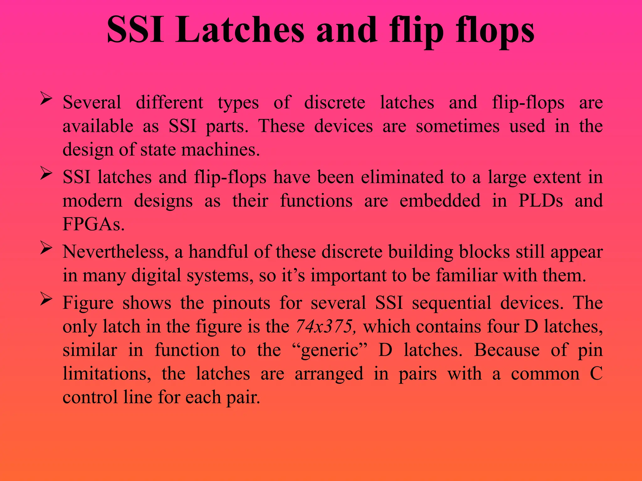
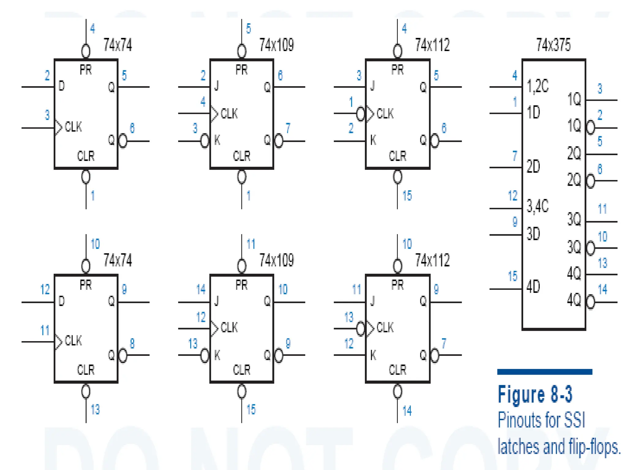
SSI Latches and flip flops
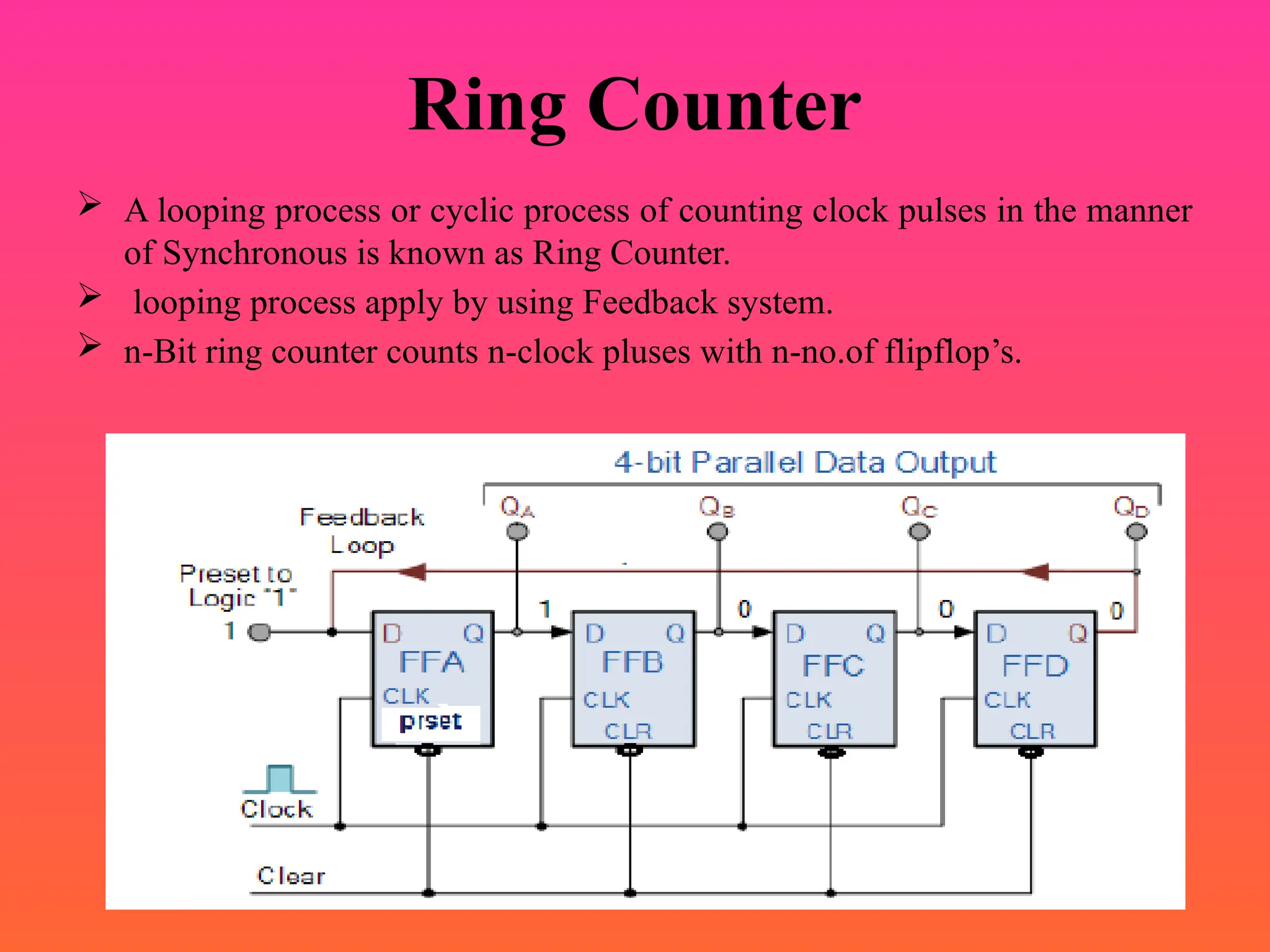
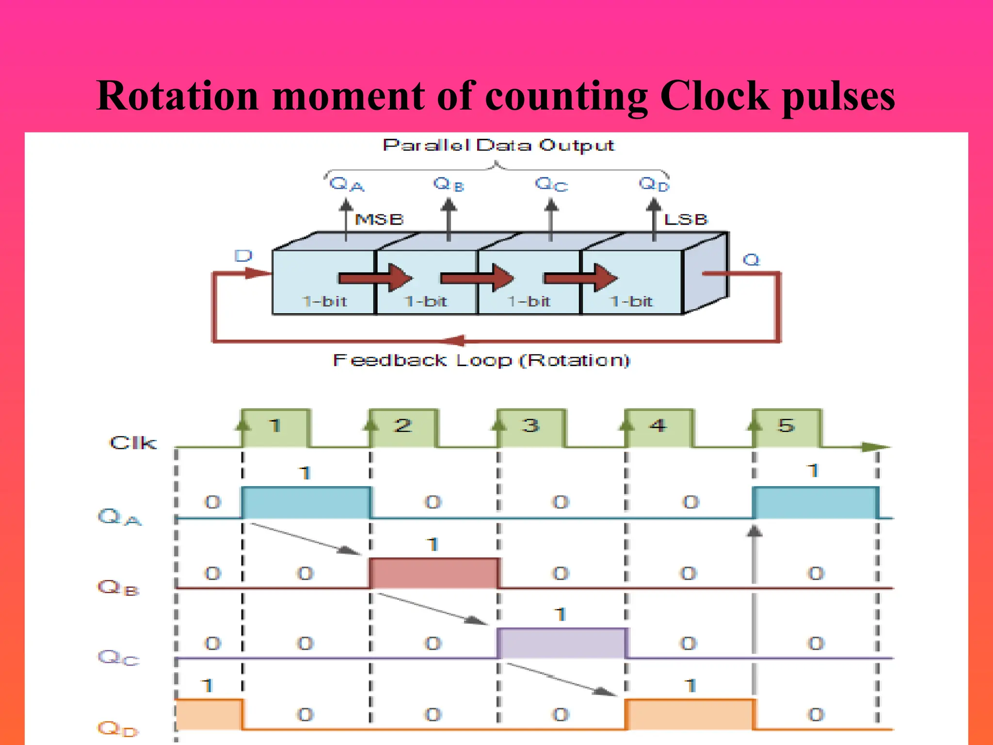
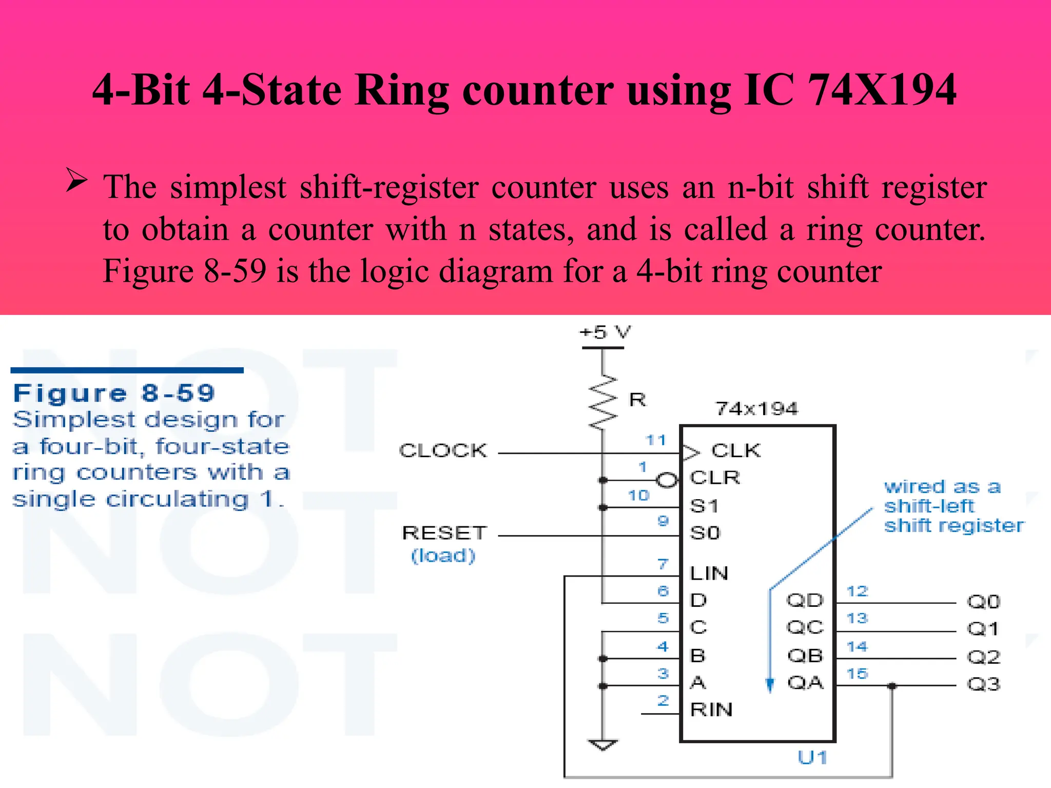
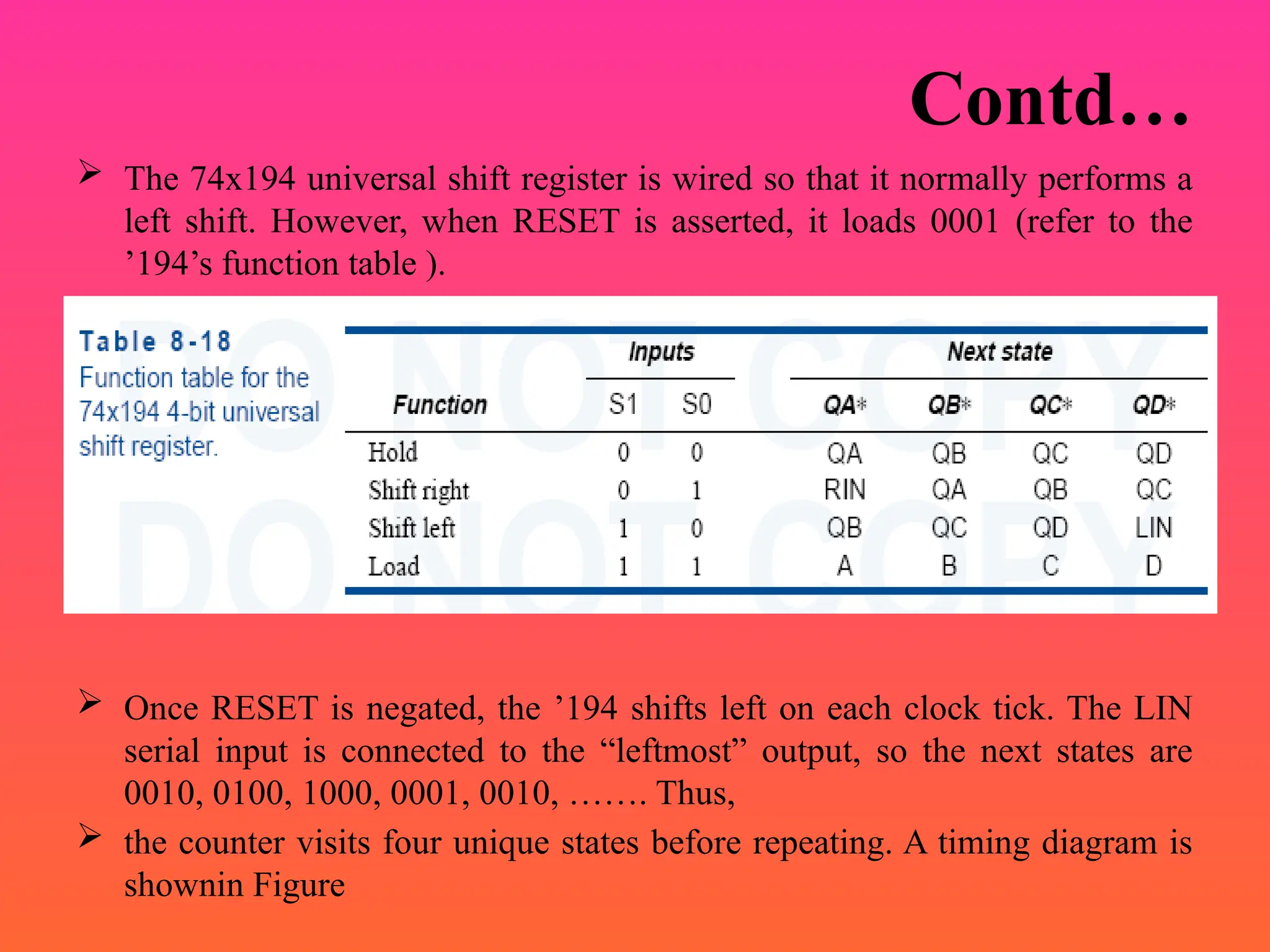
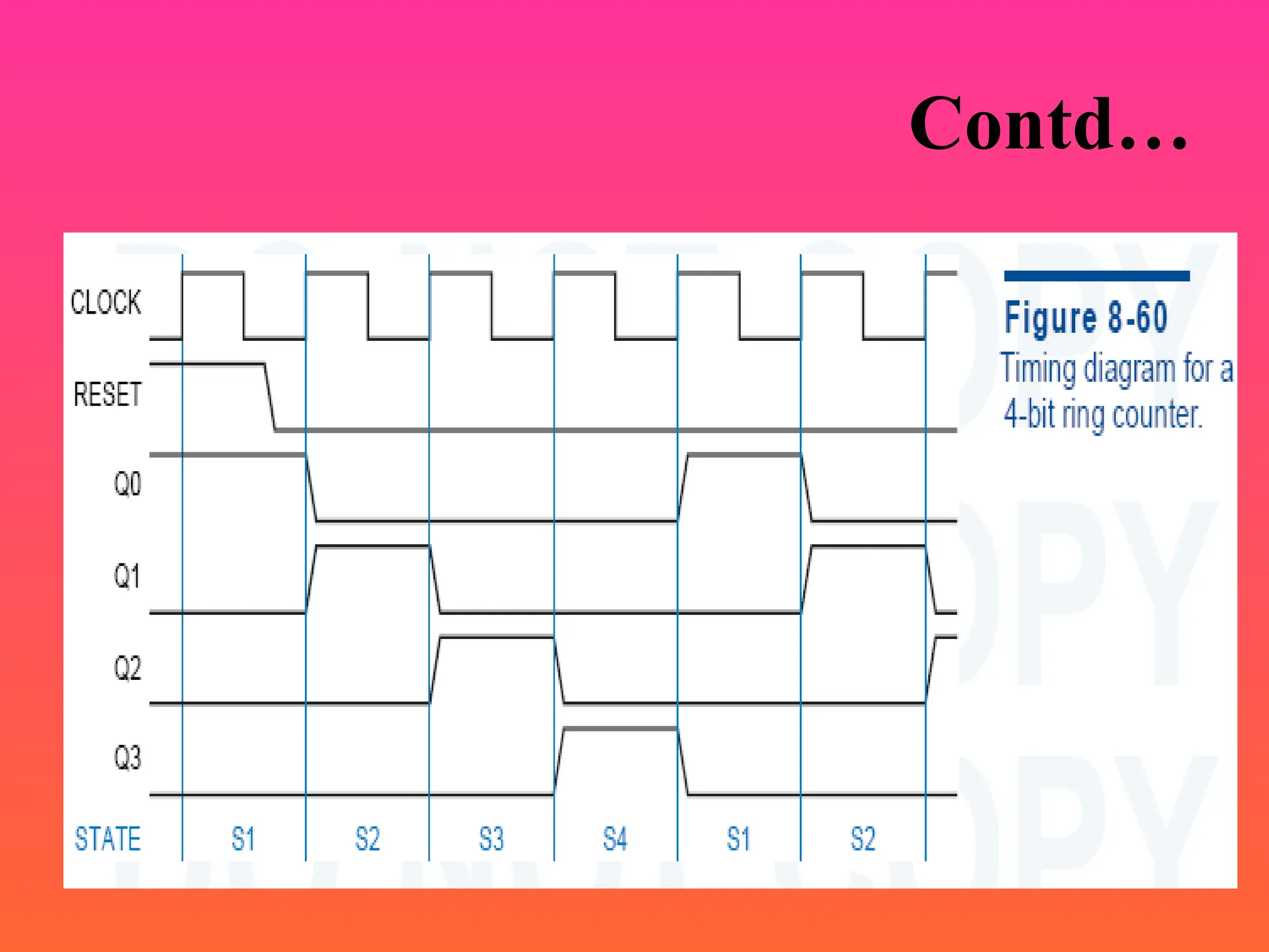
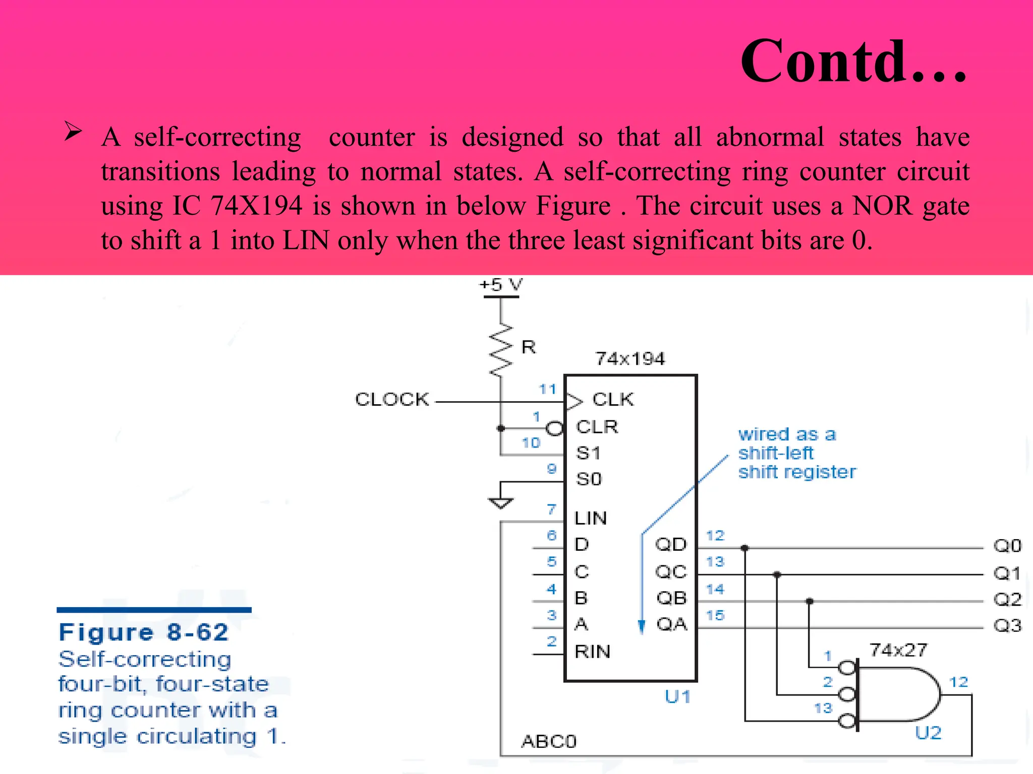
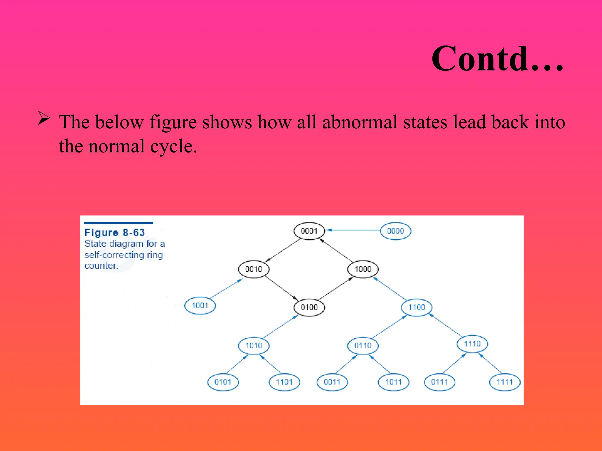
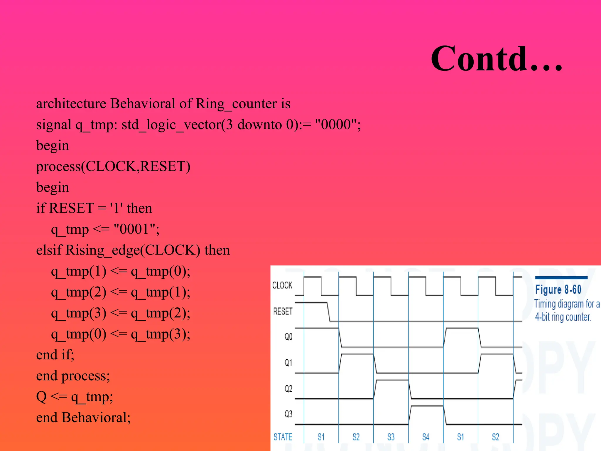
Ring Counter
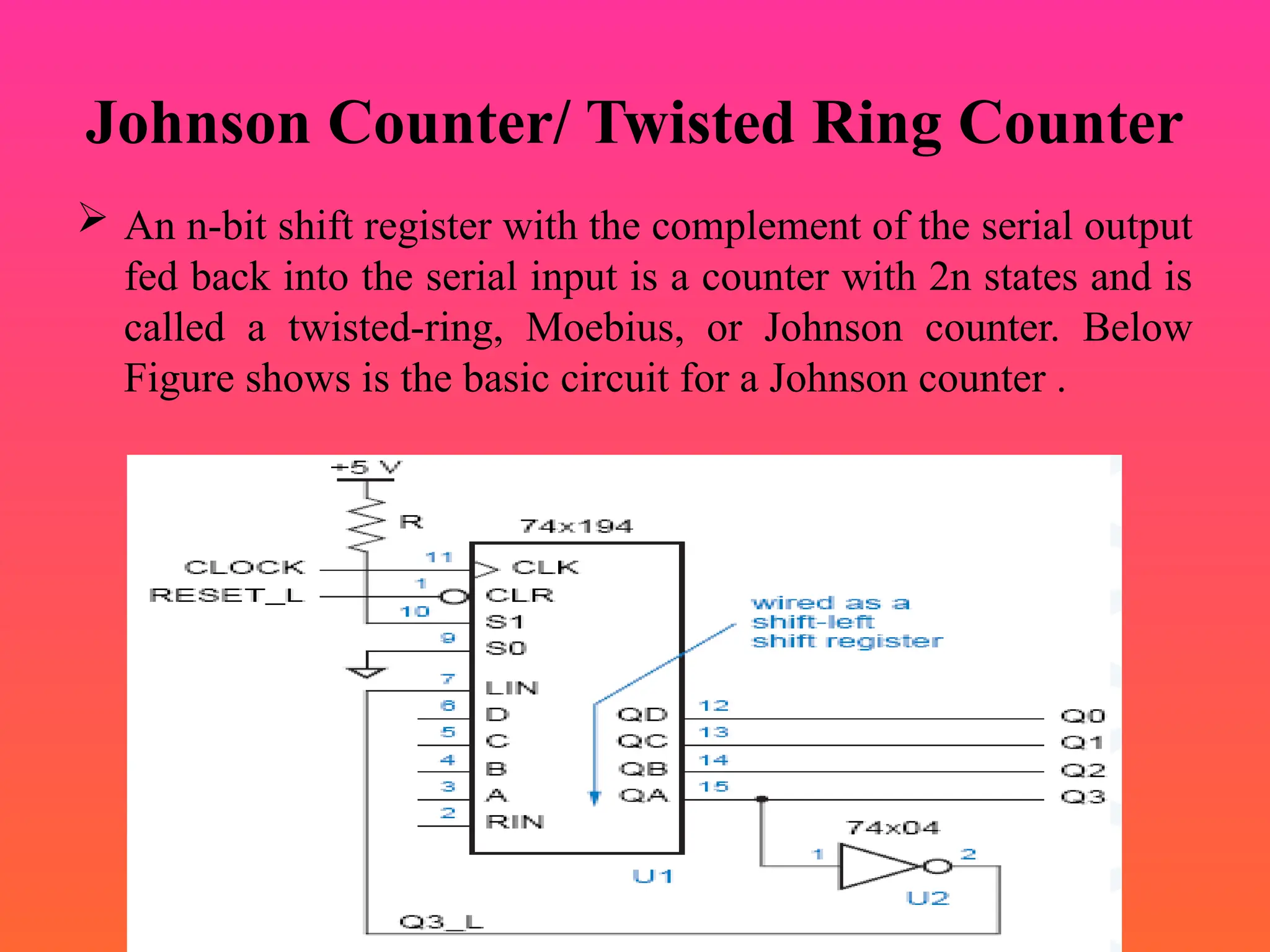
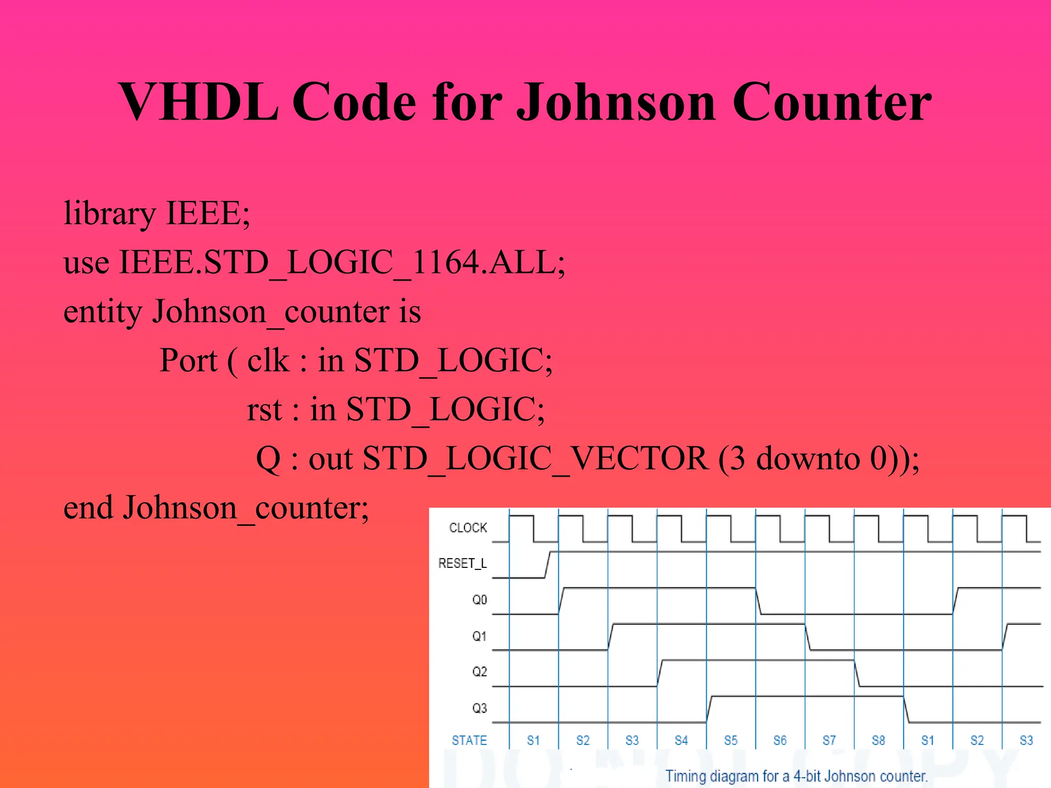
Johnson Counter
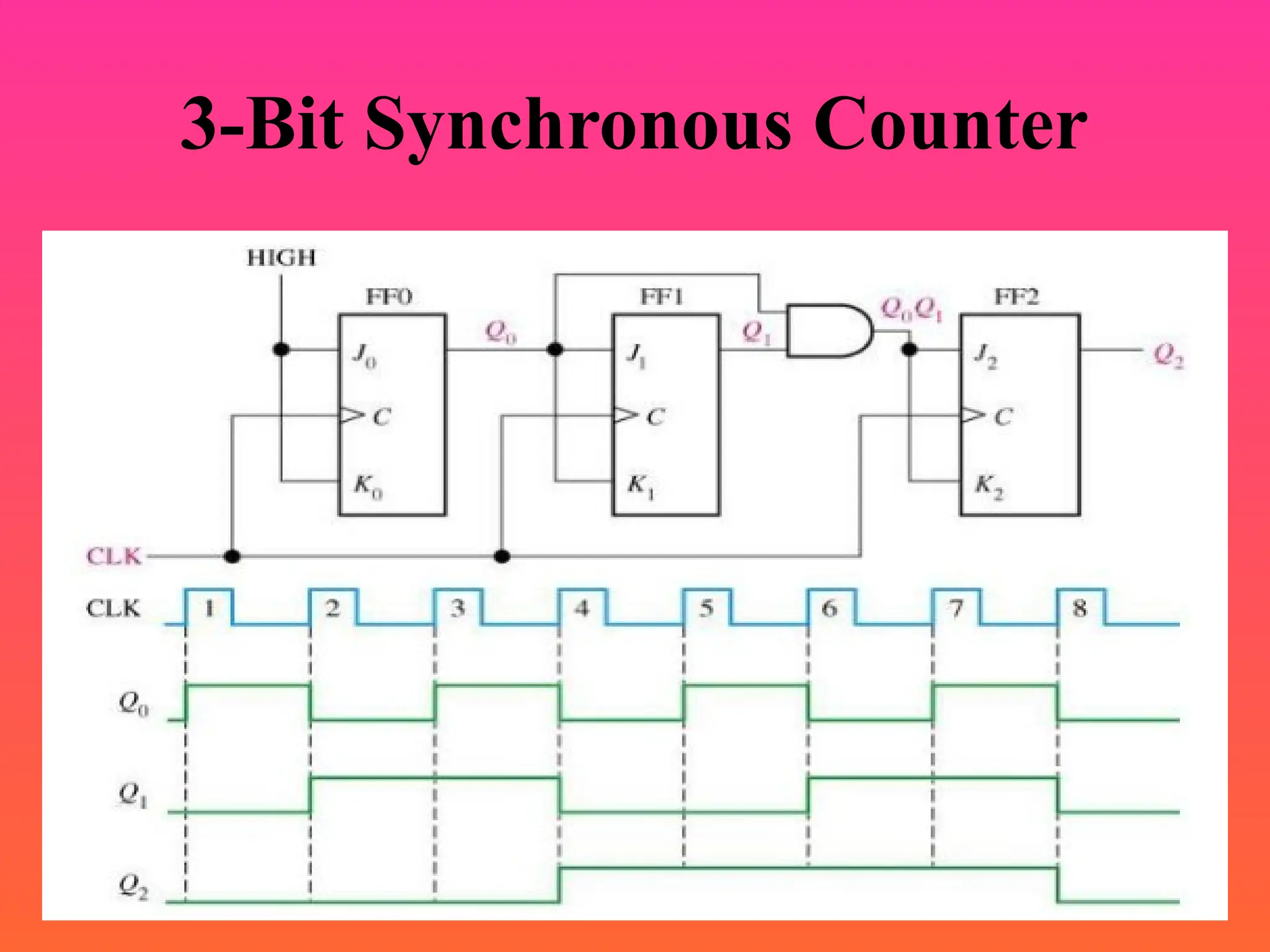
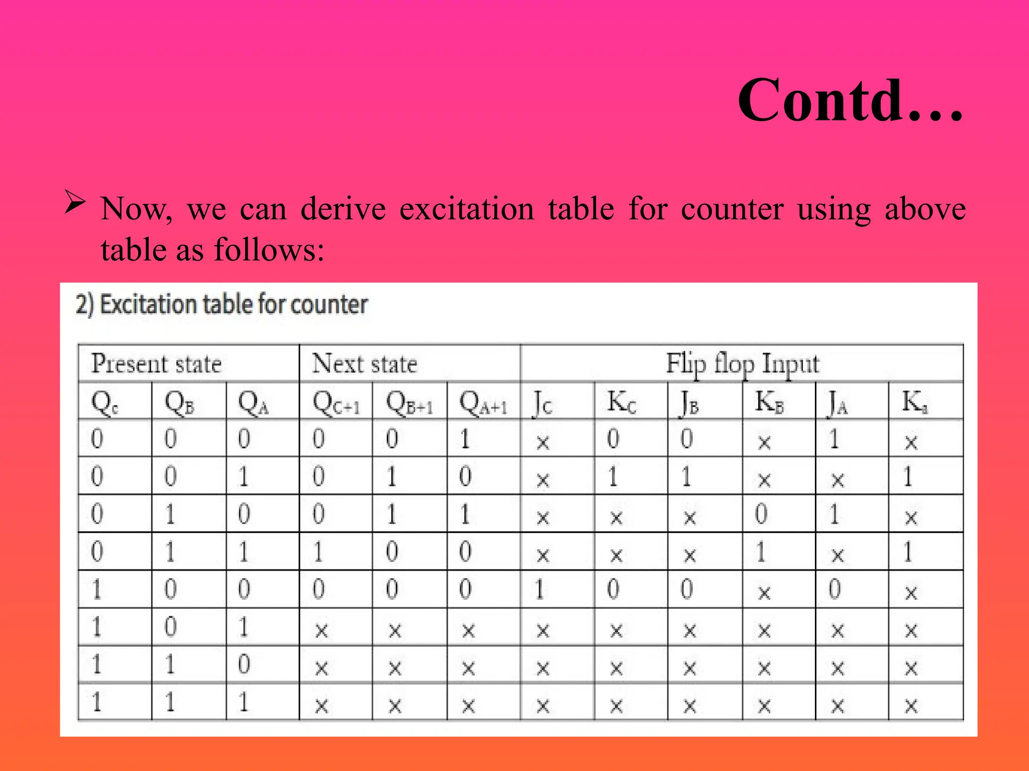
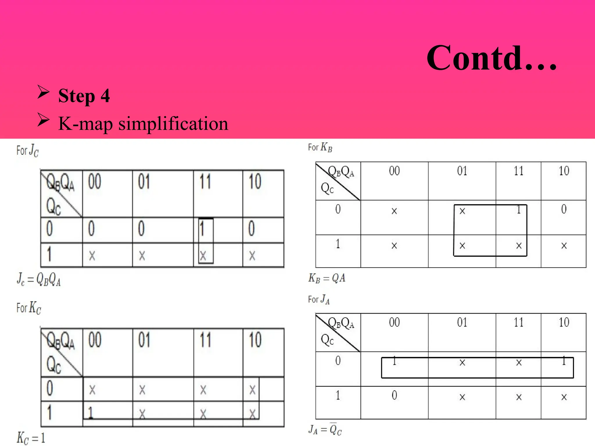
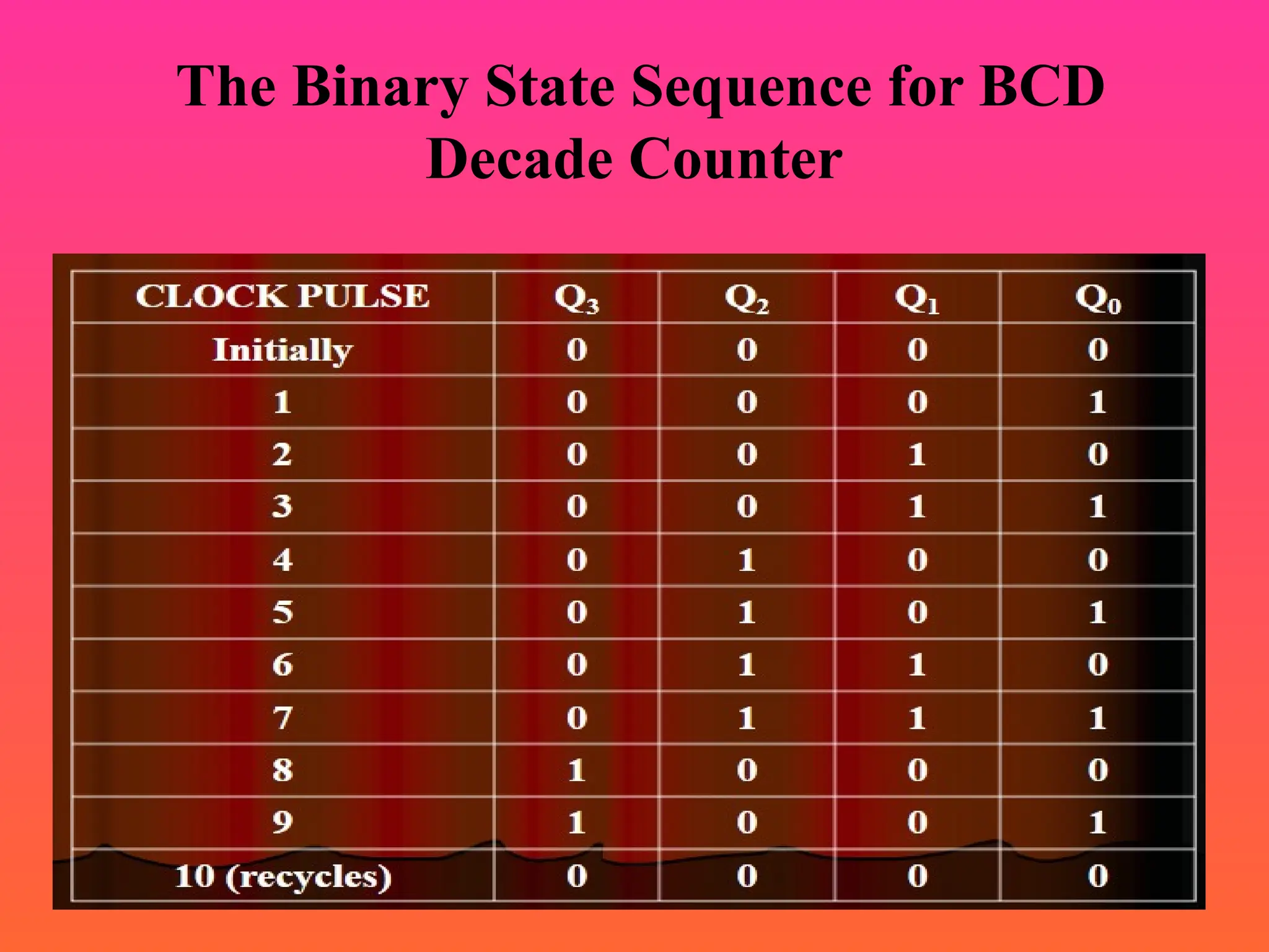
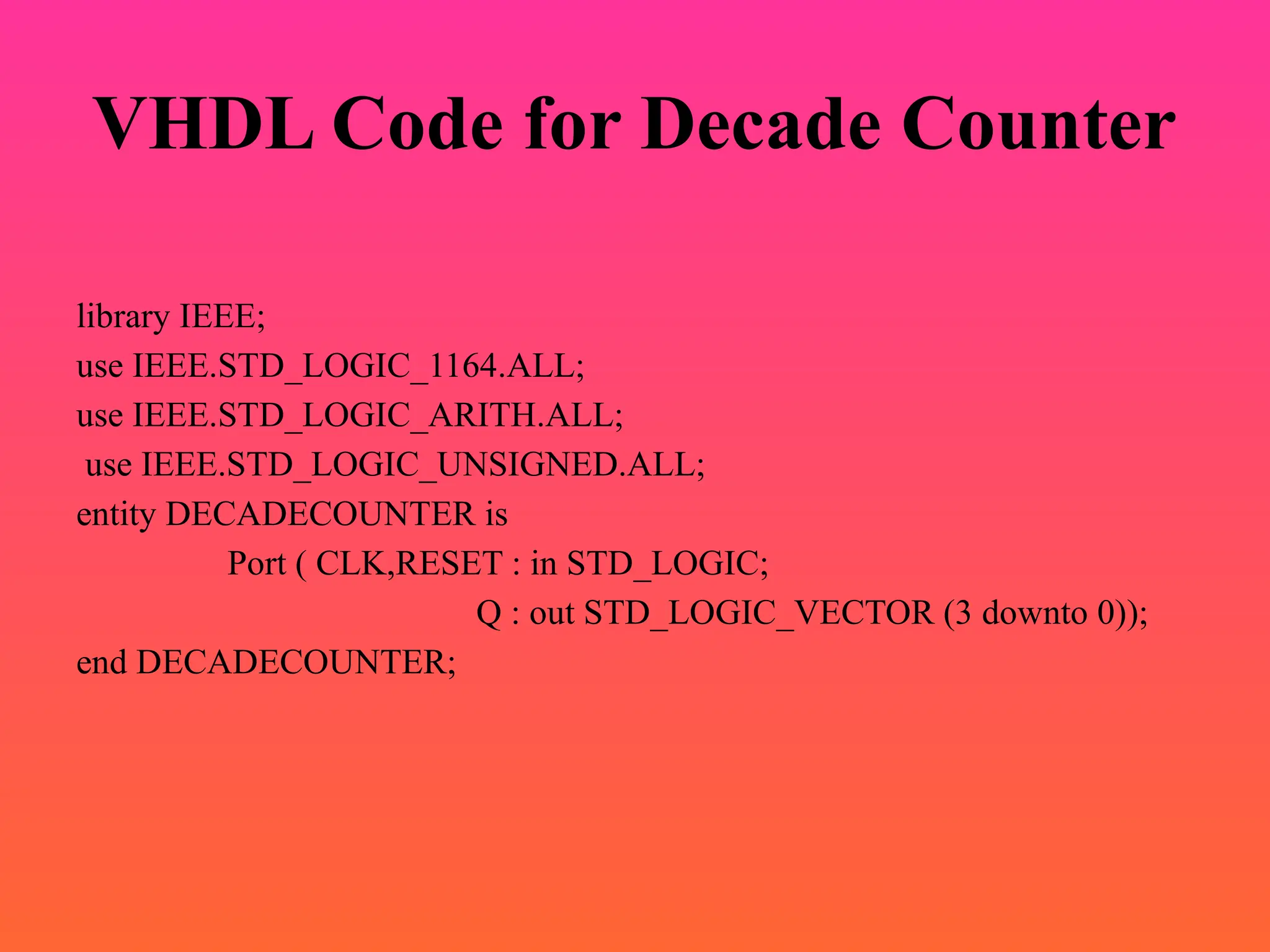
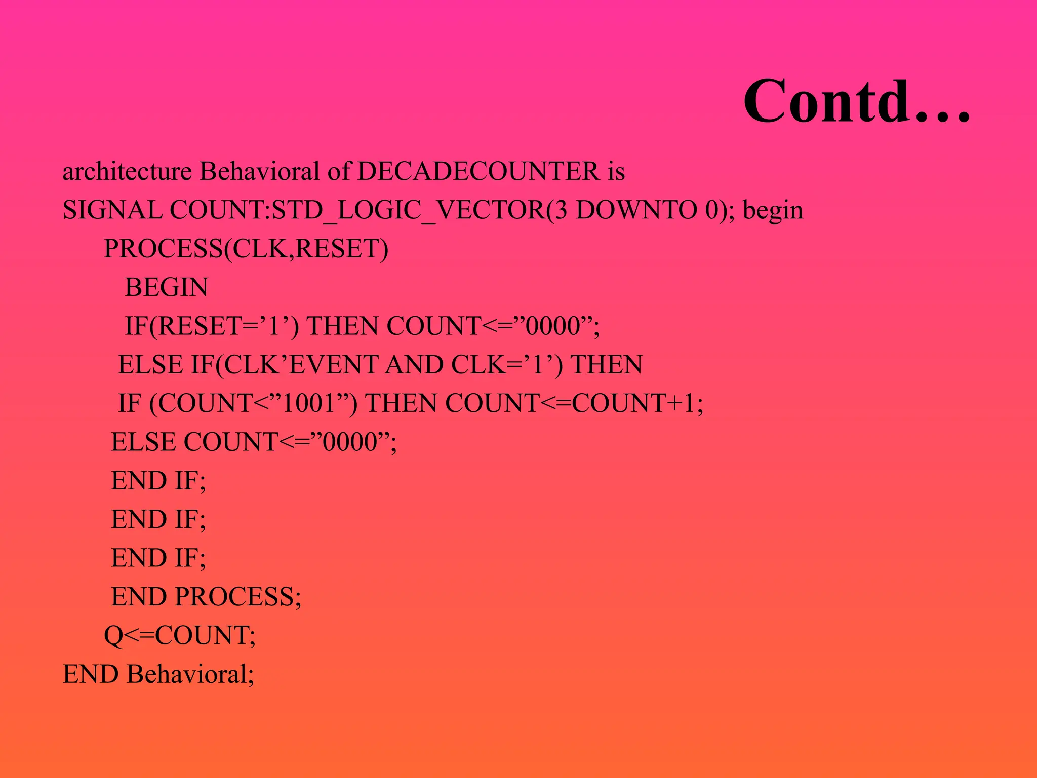
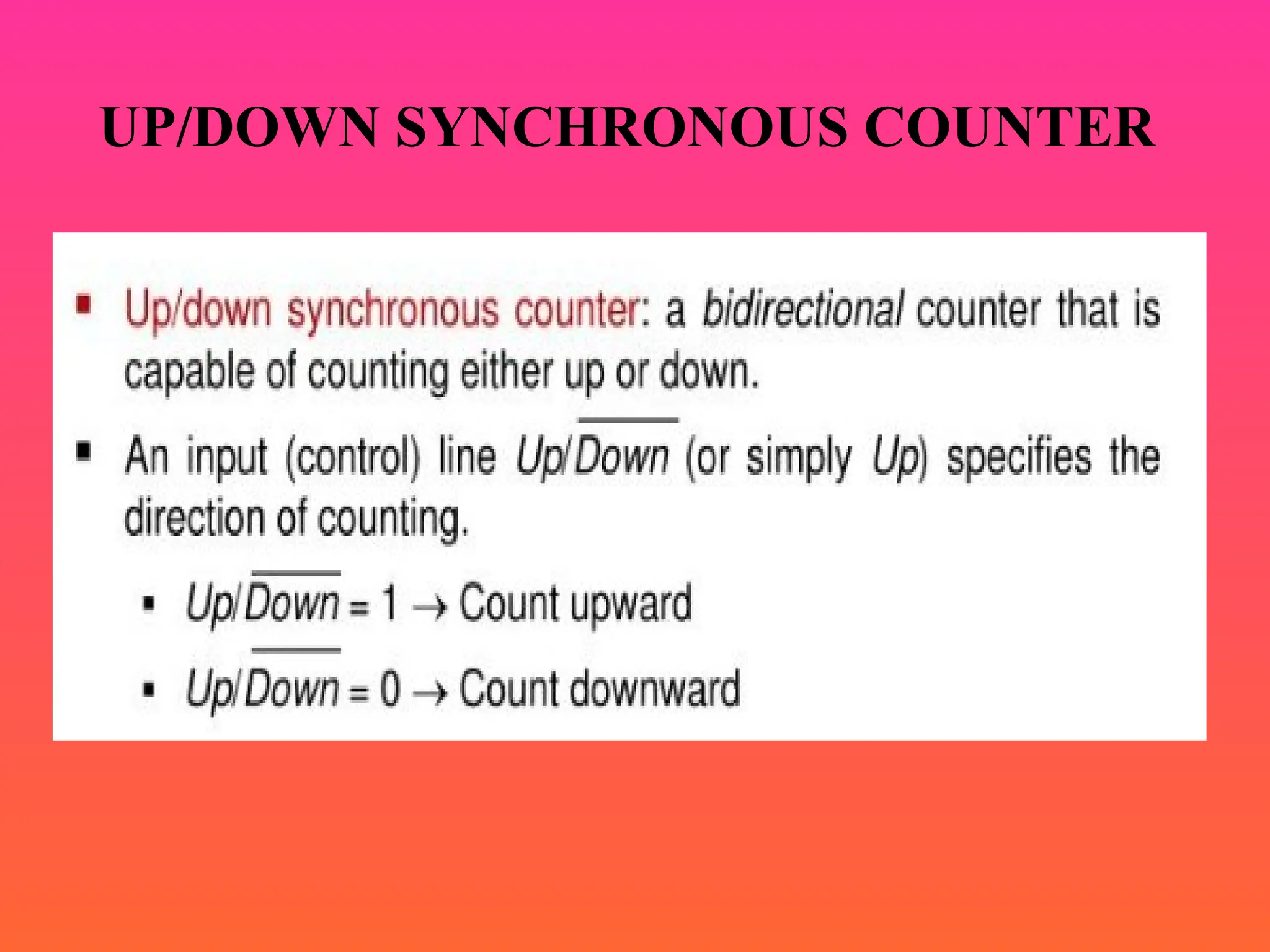
Design of Modulus N Synchronous Counters
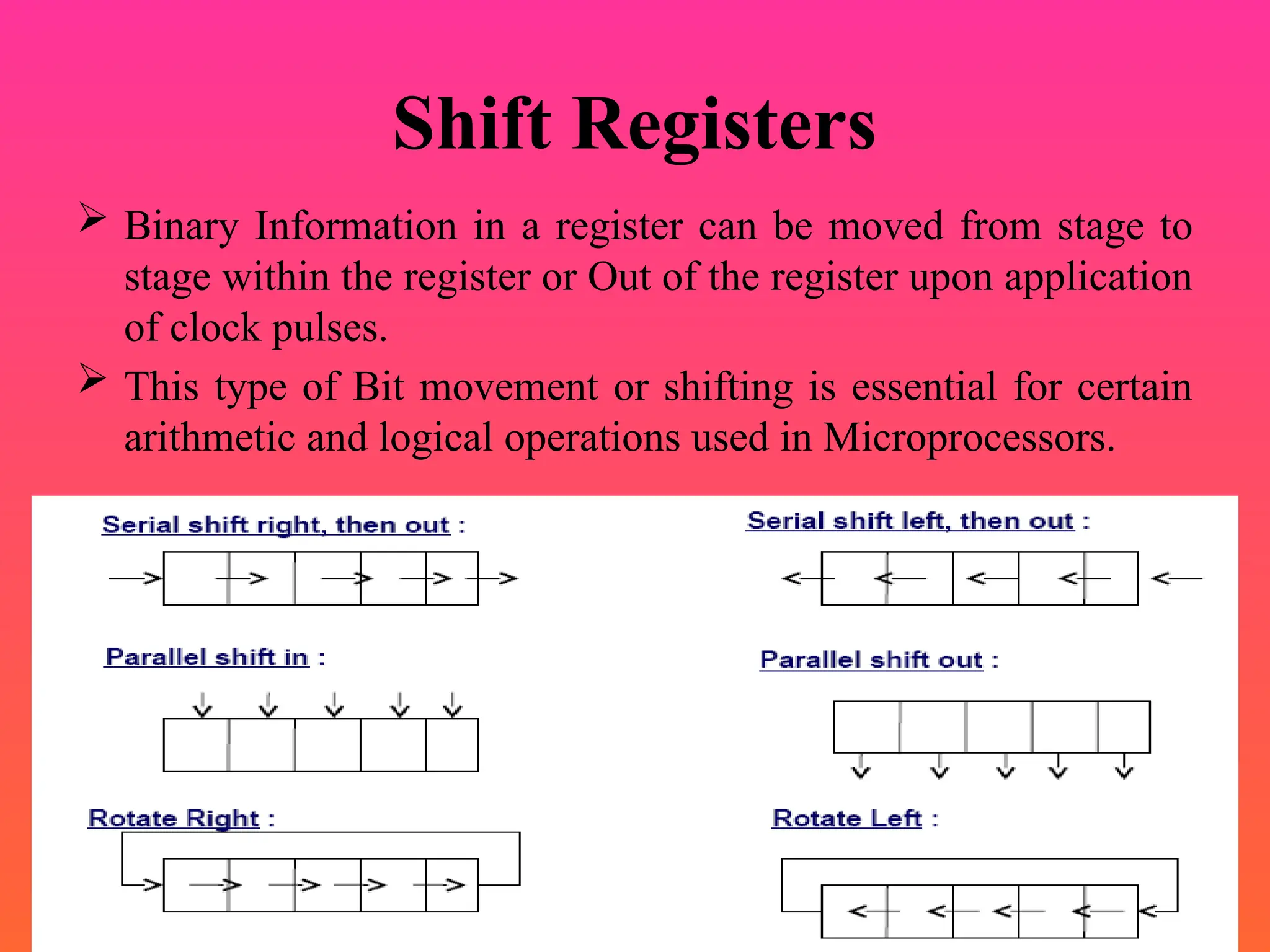
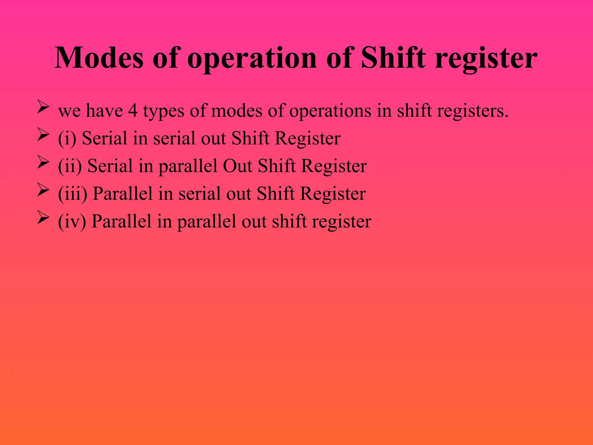
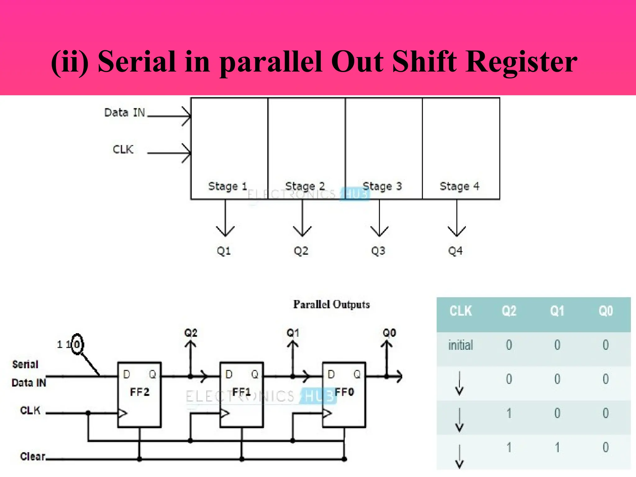
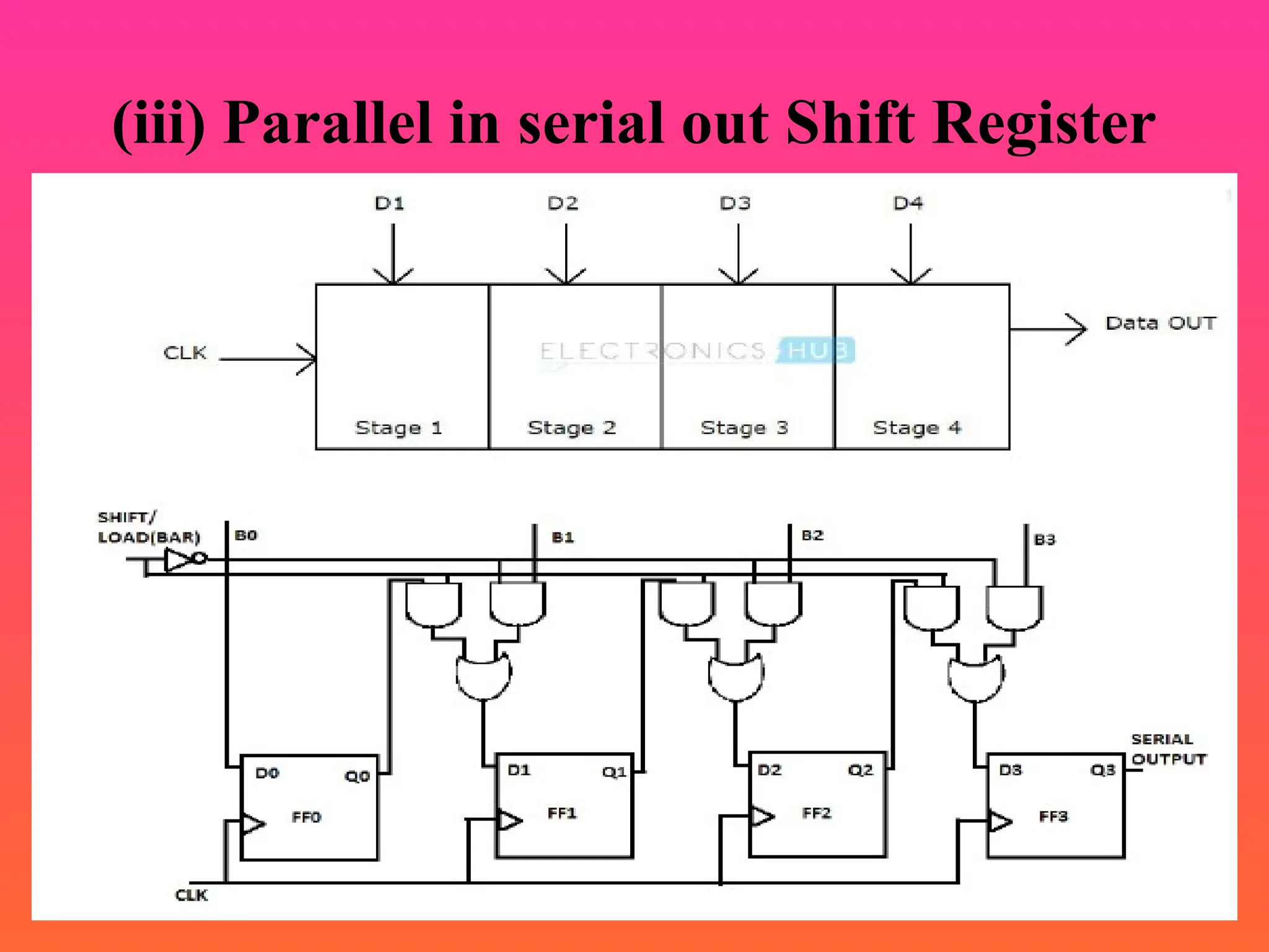
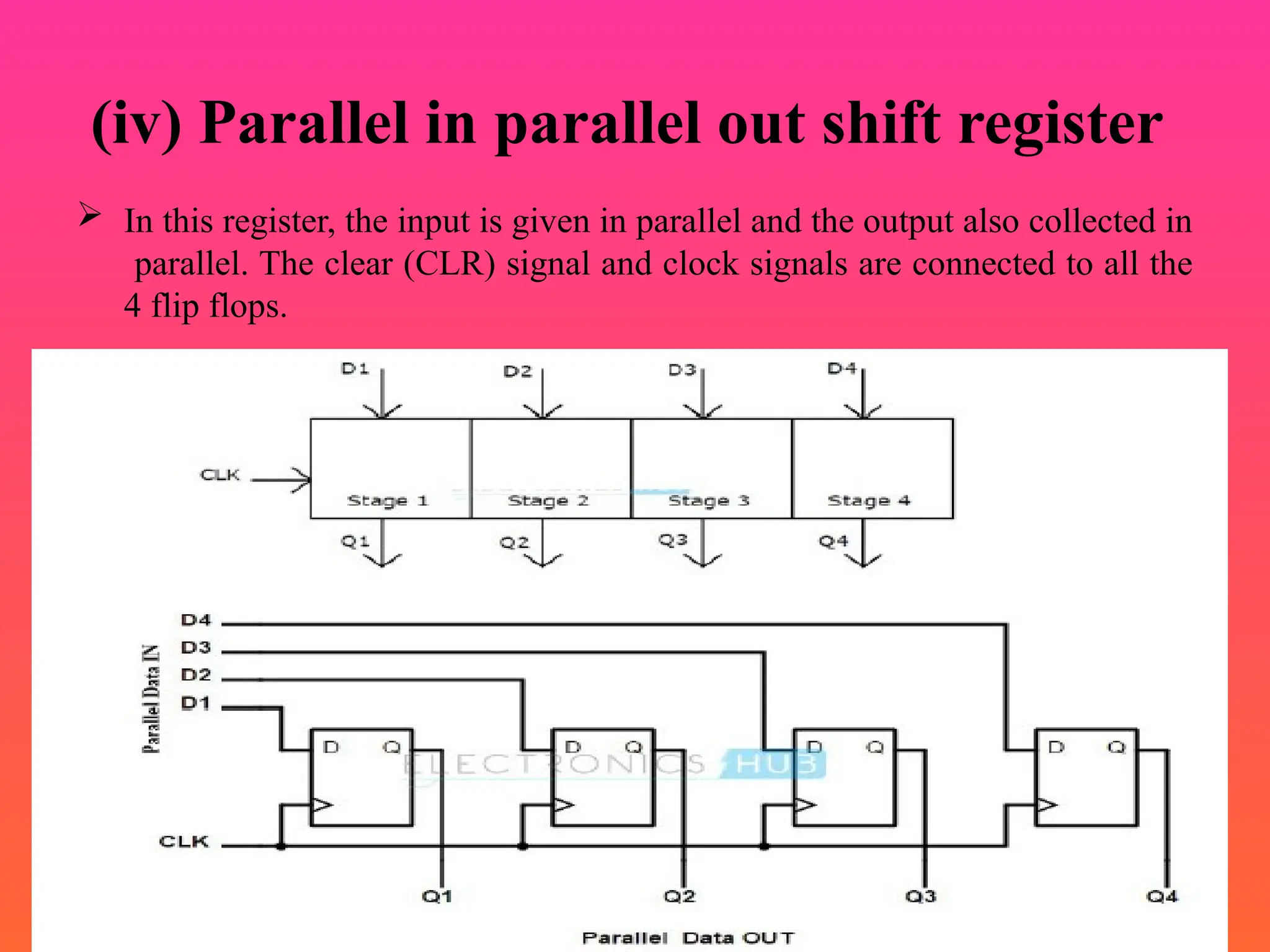
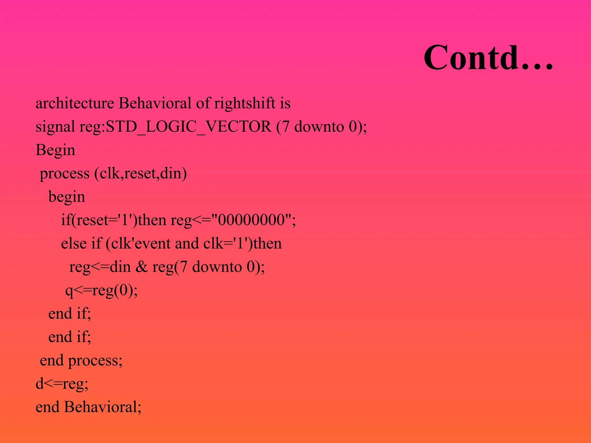
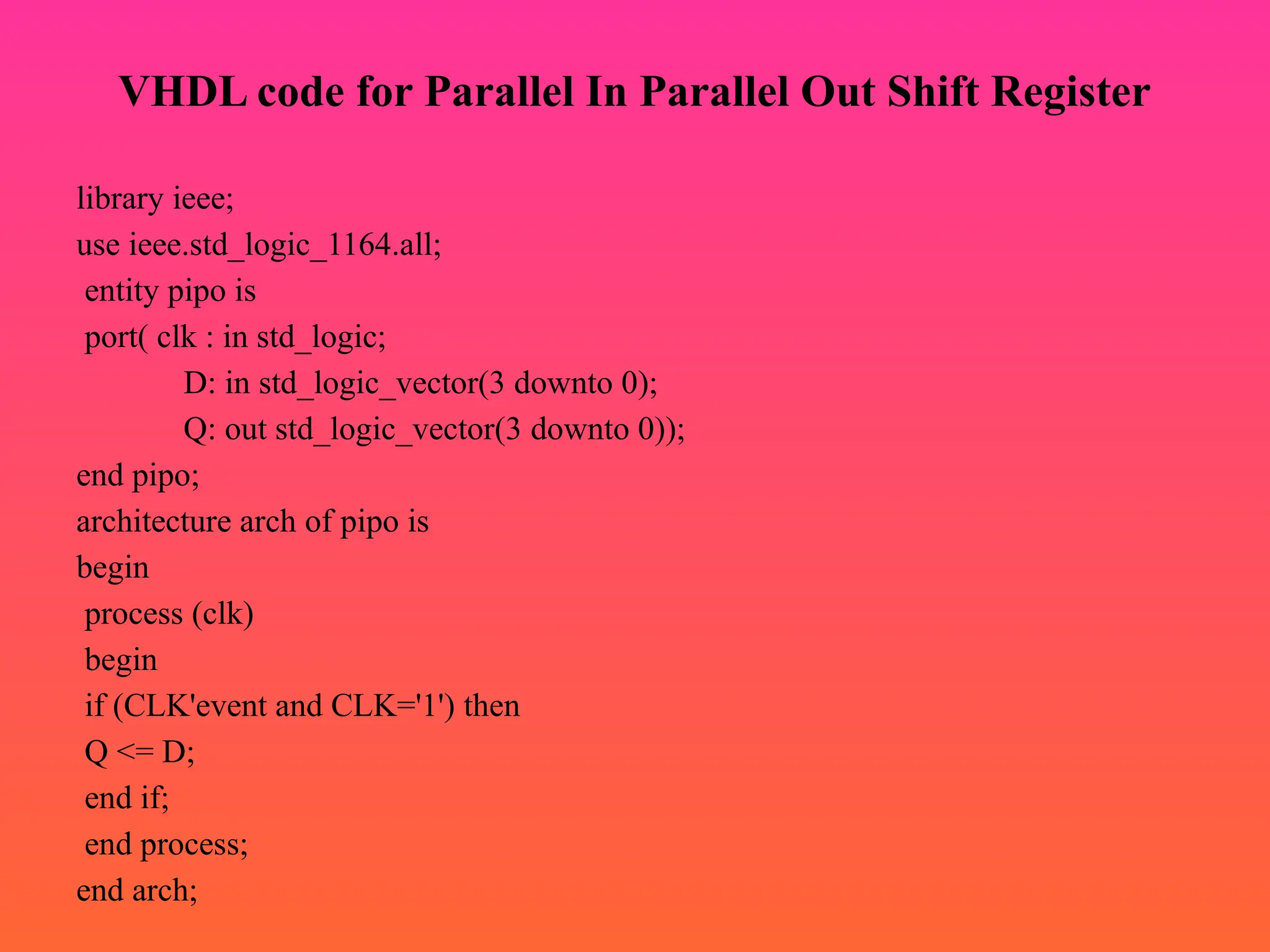
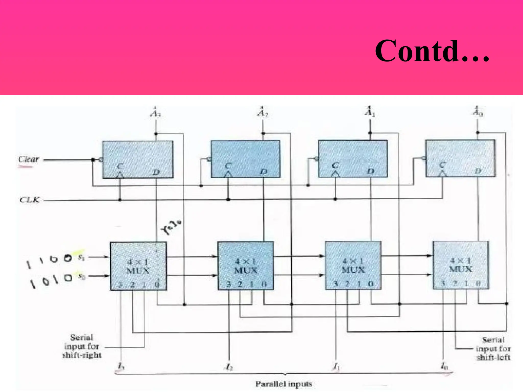
Shift Registers
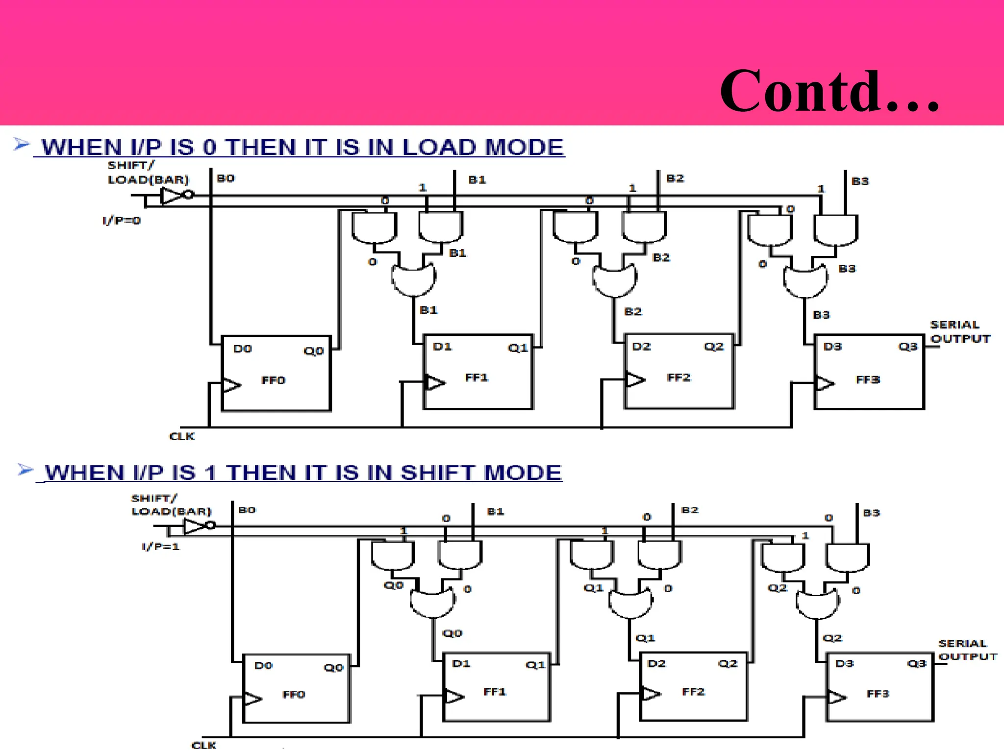
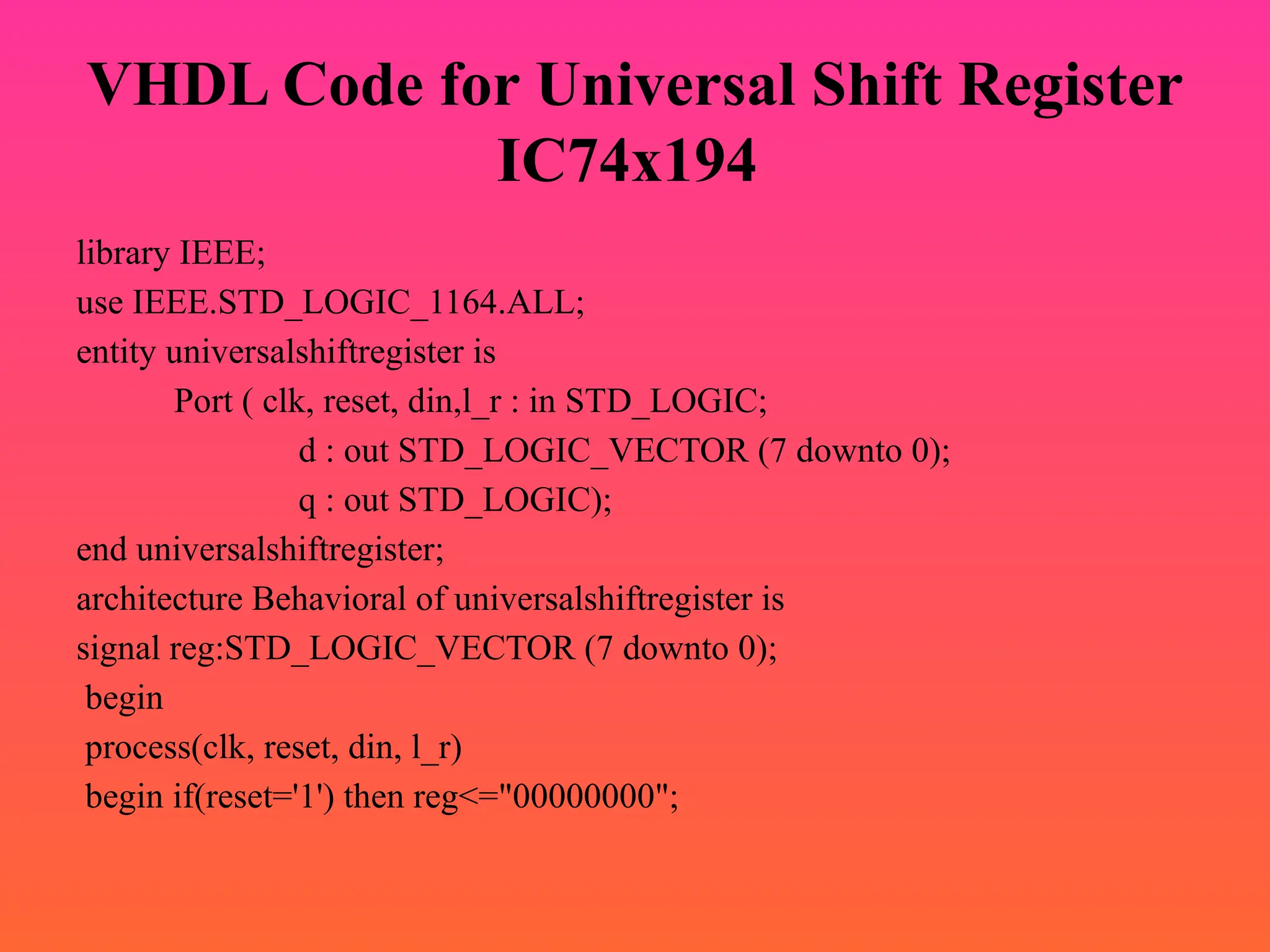
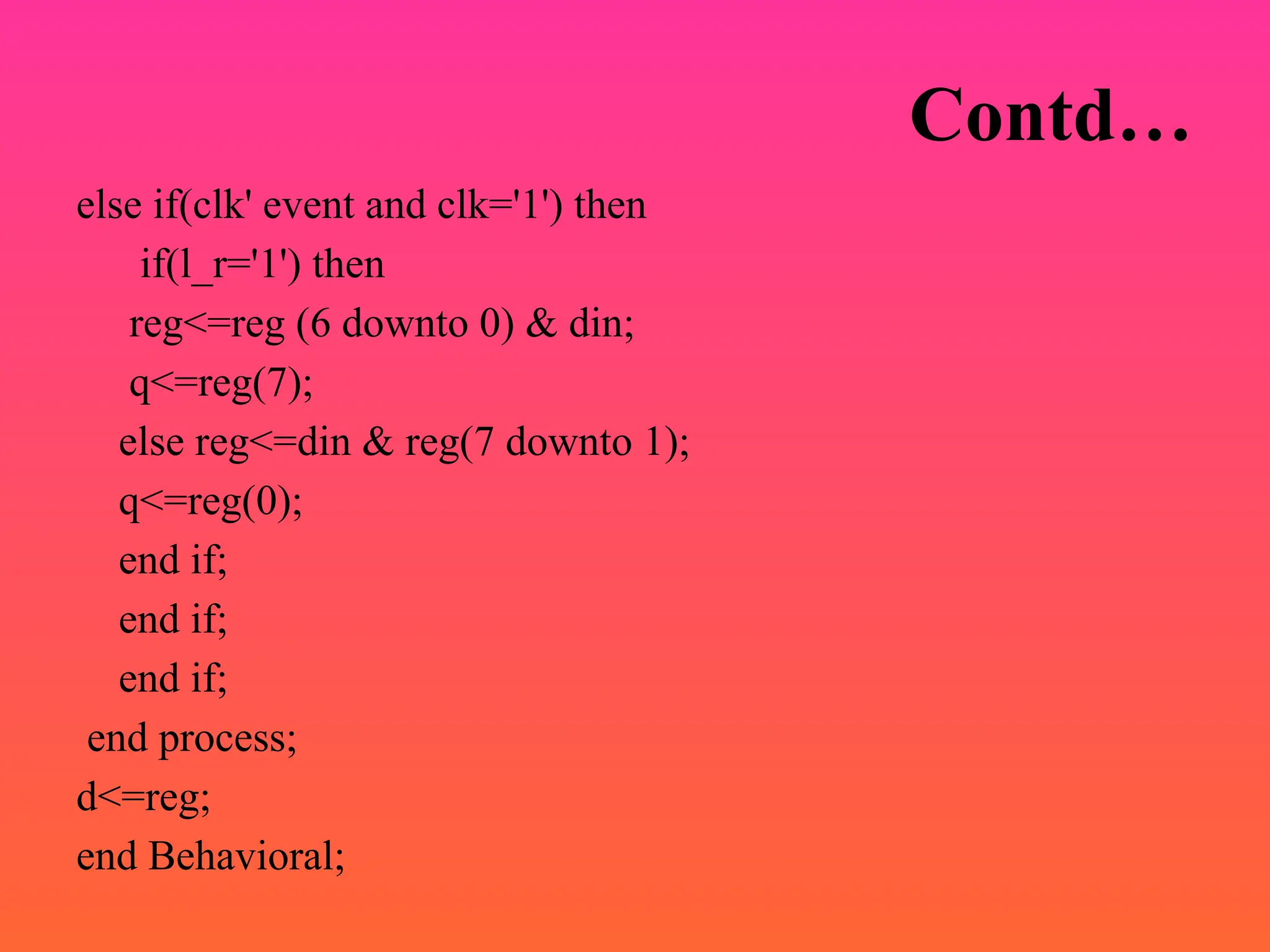
Universal Shift Registers
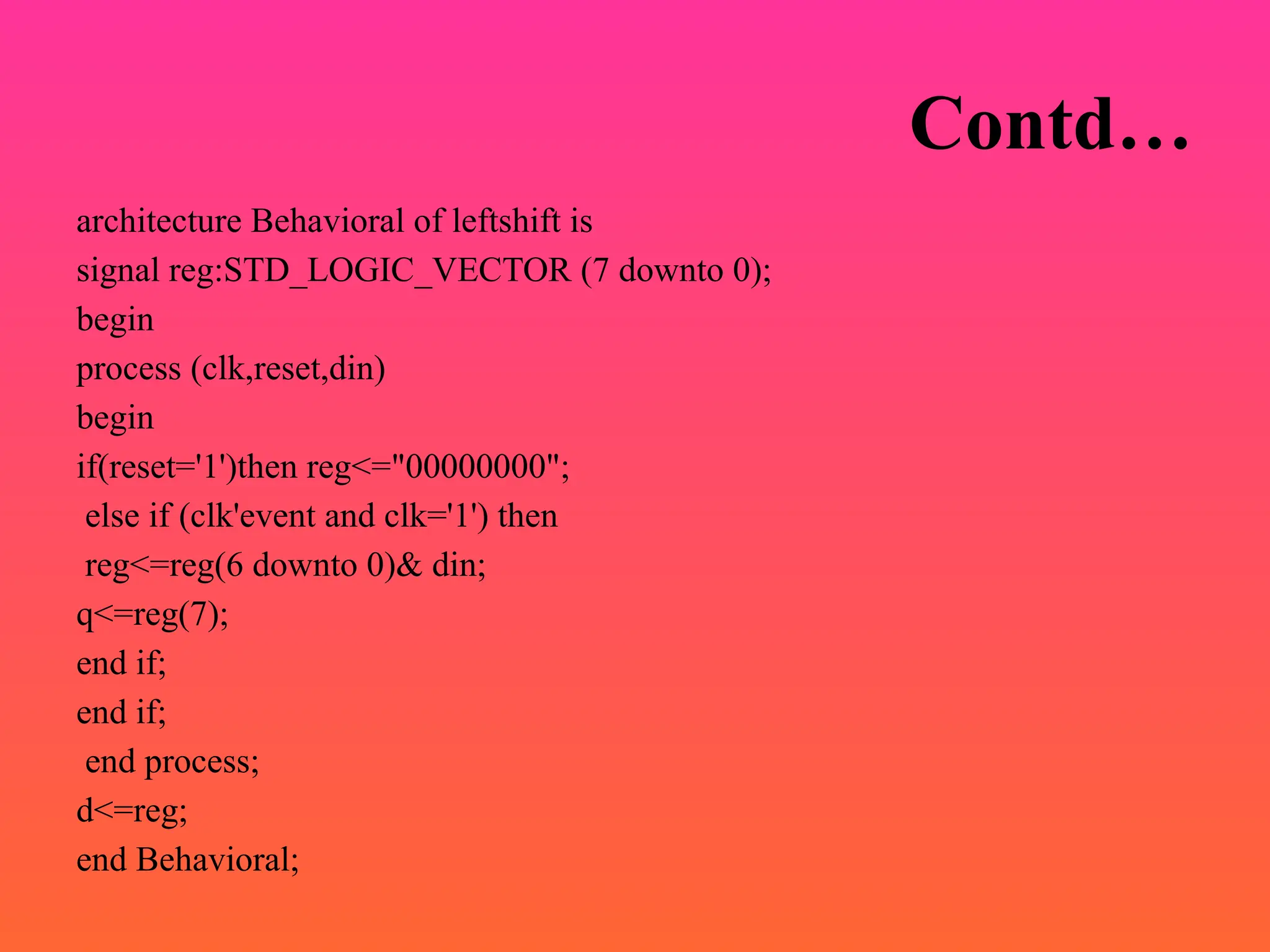
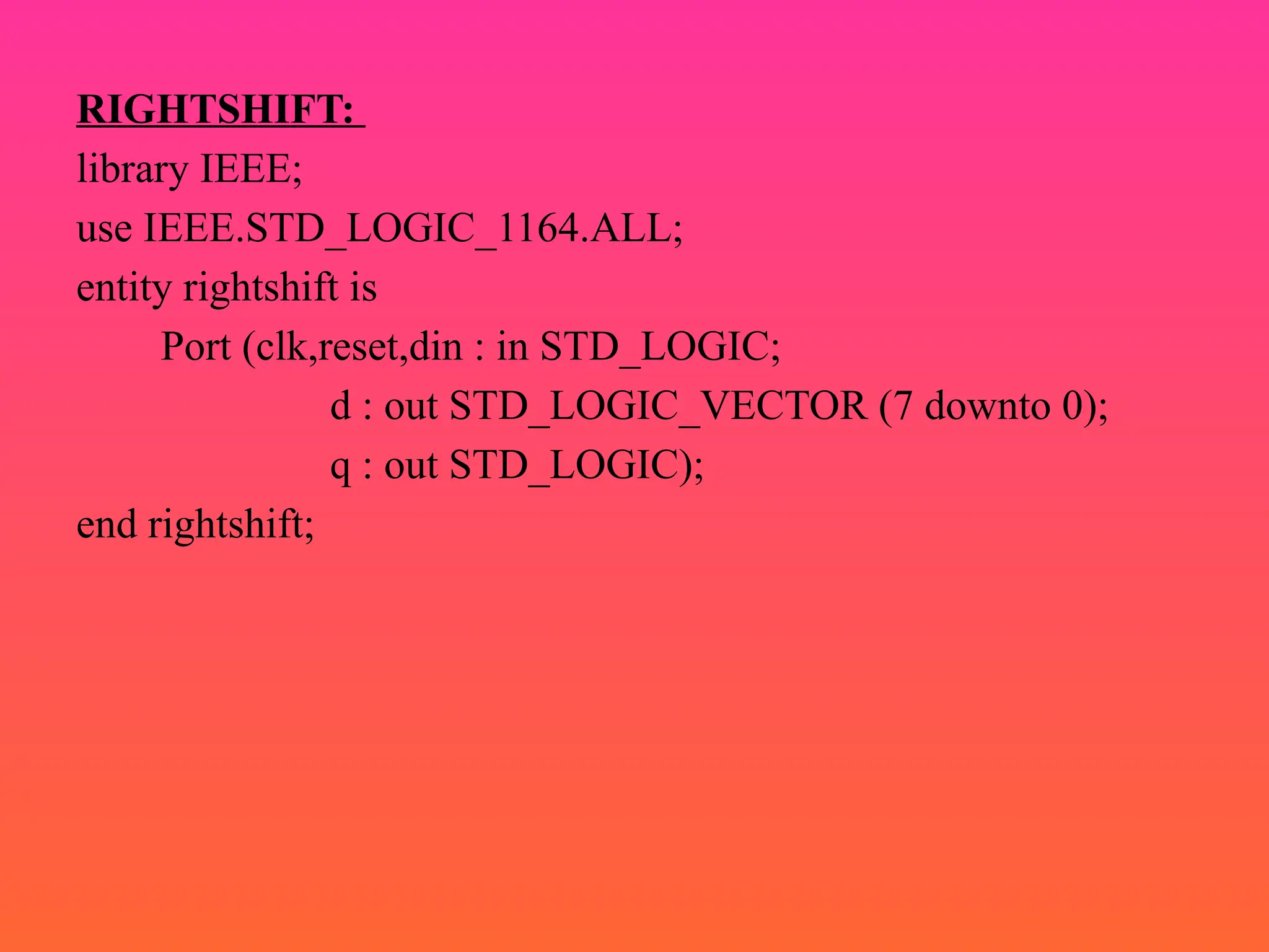
Design considerations of the above sequential logic circuits with relevant Digital ICs, modeling of above ICs using VHDL