Downloaded 30 times

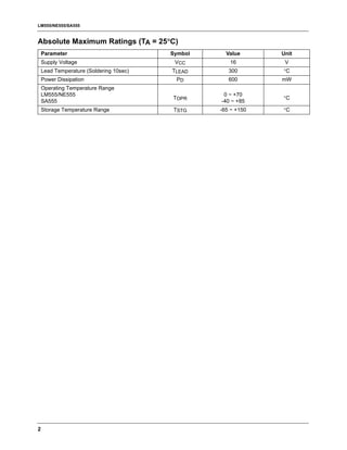
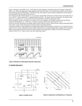
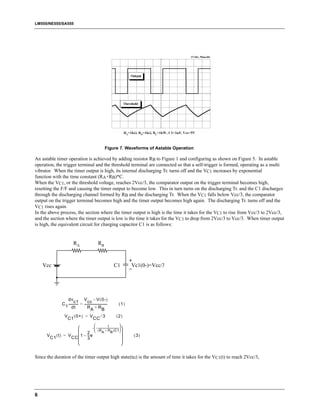
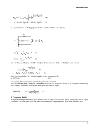
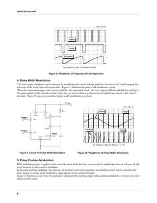


The LM555/NE555/SA555 is a highly stable single timer capable of producing accurate timing pulses from microseconds to hours. It has two main operating modes - monostable and astable. In monostable mode, it generates a single output pulse when triggered, with the width determined by an external resistor and capacitor. In astable mode, it produces a continuous train of pulses with adjustable duty cycle and frequency set by two external resistors and one capacitor. Key applications include precision timing, pulse generation, time delay generation and sequential timing.


